CC0402CRNPO9BN2R7中文资料
78K0 KC2 Tutorial manual

8位全闪存微控制器78K0/KC2学习板使用指南日电电子(中国)有限公司Doc.No.NECEC-TM-CA-0710-01Version 1.002007年10月责任声明:这里所介绍的78K0/KC2学习板是日电电子(中国)有限公司经过实际验证,以说明操作和应用为目的提供给客户的。
客户在设计应用时,应在自负全责的前提下进行,对于用户或第三方所导致的任何损失,日电电子(中国)有限公司不承担任何责任。
关于使用78K0/KC2学习板在您得到78K0/KC2学习板时,内部已经写入4 LED亮灯控制的程序,右图是78K0/KC2学习板的配置图,SW2开关拨到off状态时,78K0/KC2学习板工作在通常模式,上电后,即可观察到4个LED的亮灯状态。
但是,它的功能远不止这些,还可以:1.在线编程¾通过右图中的CN1-USB接口与PC连接,利用PG-FPL3控制程序,可以实现在线编程2.片上调试¾通过右图中的CN2-MINICUBE2接口与MINICUBE2连接,可以进行片上调试78K0/KC2学习板原理图Copyright ©2007NEC Electronics China Ltd.编程接口部分单片机部分uPD78F 0513d程序开发–开发工具的准备1. 获得开发工具可以从附带光盘的Development tools/K0Kx2文件夹中获得如下开发工具和相关文件:¾项目管理器:PM plus (Ver.5.20)(在ra78k0_w380_e.exe中)¾汇编包:RA78K0 (Ver.3.80)(在ra78k0_w380_e.exe中)¾C 编译器:CC78K0 (Ver.3.70)(cc78k0_w370_e.exe中)¾系统仿真器:78K0用SM+ (Ver.1.10)(在sm+for78k0_kx2_w110_e.exe中)¾编程控制文件:PG-FPL3(fpl_v110.exe)¾片上调试仿真器MINICUBE2 控制程序:ID78K0-QB(id78K0-qb_v294_e.exe)¾使用片上调试仿真器MINICUBE2 编程时的控制程序:QB-Programmer (qbp_v221_e.exe)¾设备文件:DF051344.78K (在df780547_v220.exe中)¾参数文件:78F0513d.prm(在prm78f0547_v107.exe中)上述开发工具的中文“用户指南”可以从光盘的User Manual文件夹中获得。
Han 接触器手动紧固工具及相关产品参数说明书

90·1ContentsPage Hand crimping tools for Han ® standard contacts .....................................90.4Hand crimping tools for fibre optic contacts .............................................90.9Hand crimping tools for Han-Fast ® Lock contacts ...................................90.10Hand crimping tools for wire end ferrules ................................................90.11Hand crimping tools for D-Sub contacts ..................................................90.12Hand crimping tools for coaxial contacts .................................................90.13Pneumatic crimping tool ..........................................................................90.15Hydraulic crimping tools for Han ® TC high current contacts ....................90.16Crimping machine TC-C01 ......................................................................90.18Crimping machine TK-M ..........................................................................90.20Crimping machine BK ..............................................................................90.22Panel punch .............................................................................................90.24Assembly tools ........................................................................................90.25Removal tools ..........................................................................................90.29Stripping tools ..........................................................................................90.32ToolsHan ® tools1) TK-M basic machine 09 98 000 6900 is required2) depending on the wire3) only with modification 09 98 503 6900Features• Basic unit of compact construction for pre-stripped wires (stranded wire)• Easy handling due to well-arranged design• for individual, turned male and female contacts• Selective processing of male and female contacts• Automatic contact feed• Reproducible, top quality gas-tight crimp connections• Non-slip, anti-vibration adjustable feet for setting the height • Low noise level• With carrying handle• Removable electric and pneumatic supply connections • Maintenance interval counter• Minimal setup effort• Stepless adjustment of the crimping depth• Low follow-up costs for maintenance and repair• Easy replacement of wearing components DetailsNominal voltage, max. 230 VNominal frequency 50 HzPower consumption ca.0.2 kWPressure ca.6 barControl system PLCWork cycle trigger FootswitchWork cycle 1 sNoise level ca.62 dBCrimp type Four-point crimpingContact feed Vibratory bowl feedStroke counters Resettable daily counter and permanent counterDimensions 345 x 230 x 400 mmWeight ≥24 kgPack contents:2.0 m connection cable and grounding plug, 2.0 m pneumatic hose,quick-release coupling and N6 plugin nipple, footswitch,carrying handle,operating instructions,declaration of conformityTools90Features• Basic unit of compact construction• Fast stripping and crimping in one operating step• Easy handling due to well-arranged design• Touchscreen controlling• for individual, turned male and female contacts• Selective processing of male and female contacts• Contact magazine with filling control• Reproducible, top quality gas-tight crimp connections• Infinitely variable adjustment parameters (stripping depth, stripping length, crimping depth, crimp contact feed rate)• Rotatable vibration feeder and actuator in basic unit• Low noise level• for oil-free compressed air• Minimal setup effort• Low maintenance costs DetailsDrive electro-pneumaticNominal voltage, max. 230 VNominal frequency 50 HzPower consumption ca.0.75 kWPressure ca.6 barCompressed air connection 3 dm³ / work cycleControl system PLCWork cycle trigger sensorWork cycle 1.5 sNoise level <70 dBCrimp type Four-point crimpingContact feed Vibratory bowl feedStroke counters Resettable daily counte, total counter, operating hours, maintenance counter and quantity preselection Dimensions 580 x 470 x 470 mmWeight <60 kgPack contents:one mounted interchangeable unit,2.0 m connection cable and grounding plug,2.0 m pneumatic hose with plug-in nipple N6,plug gauges for setting the crimping,centering bush for positioning the plug gauges,draw for insulation remains,drawer for holding the contacts when the magazine is emptied, tool set for setting,1 set of stripping blades,operating instructions,declaration of conformityToolsCrimping machine TK-M90Features• Fast stripping and crimping in one operating step• Easy handling due to quick change tool and stripper• Suitable for standard D-Sub crimp contacts• Selective processing of male and female contacts• Hand wheel for manual adjustments• Maintenance-friendly through needle bearing rail• Automatic exhaust of the isolation remainders• Reproducible, top quality gas-tight crimp connections• With crimp force monitor• Setting parameters with raster rotary button (depth of insula-tion stripping, length of insulation stripping, crimping heigth on wire, crimping heigth on isulation, wire retainer position, band thrust and wire position in the crimp contact)• Non slip and anti-vibration feet• Low noise level• for oil-free compressed air• Low maintenance costs• V-blades for special wires on request DetailsDrive electro-pneumaticNominal voltage, max. 230 VNominal frequency 50 HzPower consumption 0.75 kWPressure 6 barControl system PLCStripping device type 514Suction apparatus 2000.0900.20Work cycle trigger sensorWork cycle 0.35 sNoise level 85 dBIllumination integrated tool light 20001326Motor speed 440 –2000 rpmStroke counters Resettable daily counter and permanent counter Dimensions 690 (with a contact reel: 1400) x 420 x 430 mm Weight <72 kgPack contents:with role owner and guide plate,2.0 m connection cable and grounding plug,2.0 m pneumatic hose with plug-in nipple N9,oiler bottle for the lubricating of the crimping contacts,tool set for setting,1 set of stamps for wire and isolation-crimp,1 anvil one-piece for wire and isolation-crimp,1 set of stripping blades,1 litre of contact oil,operating instructions,declaration of conformityTools90。
3CRWE62092AB中文资料

Simple—YetAdvanced3COM ®11 MBPS WIR ELESS LAN ACCESS POINT 60003Com Corporation, Corporate Headquarters, 5500 Great America Parkway, P .O. Box 58145, Santa Clara, CA 95052-8145.To learn more about 3Com solutions, visit . 3Com Corporation is publicly traded on Nasdaq under the symbol COMS.Copyright © 2003 3Com Corporation. All rights reserved. 3Com, the 3Com logo, and XJACK are registered trademarks of 3Com Corporation. Possible made practical is a trademark of 3Com Corporation. Wi-Fi is a trademark of the Wireless Ethernet Compatibility Alliance. All other company and product names may be trademarks of their respective compa-nies. While every effort is made to ensure the information given is accurate, 3Com does not accept liability for any errors or mistakes which may arise. Specifications are subject to change without notice.400747-004 01/03Product Name Region Order Number3Com 11 Mbps Wireless LAN Access Point 6000US and Canada 3CRWE60092AEurope and Latin America 3CRWE60092A-E1Asia/Pacific Rim 3CRWE60092A-A1France and Singapore 3CRWE60092A-FRJapan 3CRWE60092A-JPSouth Korea 3CRWE60092A-SKIsrael 3CRWE60092A-ISRussia 3CRWE60092A-RUUse the 3Com 11 Mbps Wireless LAN Access Point 6000 with these 3Com products:3Com 11 Mbps Wireless LAN PC Card with XJACK ®Antenna 3CRWE62092AB 3Com 11 Mbps Wireless LAN Building-to-Building Bridge 3CRWE90096A 3Com 11 Mbps Wireless LAN Workgroup Bridge 3CRWE83096A 3Com Network Jack Multiport Power-over-Ethernet Midspan Solution 3CNJPSE24Ordering Information Performance Connection speeds up to 11Mbps within a range of 100meters (328 feet)65 simultaneous user support Dynamic rate shifting between 11, 5.5, 2, and 1 Mbps as condi-tions and distances change Embedded DHCP server auto-matically assigns IP addresses,ensuring users always have a valid IP address. In instances with existing on-site DHCP server, the access point’s DHCP server recognizes this and acts as a pass through Network Management An embedded HTTP web server in each access point works with any web browser that supports XML for easy web configura-tion, firmware upgradability,and management.Standards Conformance Wi-Fi certified IEEE 802.11b Safety and Electromagnetic Conformance Safety: EN60950/A11, IEC 950,CSA22.2#950, UL 1950Radio: FCCCFR 47 Part 15.247(249) and 15.209, RSS-139,ETS 300 328, ETS 300 826,RCR STD-33Environmental: EN6068Electromagnetic compatibility:ICES-003, FCC Part 15 Class B,ETS 300 826, CISPR 22/EN55022Class B Physical Dimensions Length w/antenna perpendicular:208 mm (8.172 in)Length w/antenna parallel: 253 mm (9.966 in)Width at widest point: 144 mm (5.673 in)Height at thickest point: 41 mm (1.610 in)Height w/antenna perpendicular:84 mm (3.321 in)Environmental Operating Ranges Temperature: 0 to 55°C Humidity: 10 to 90% noncondensing Altitude: Up to 3000 m (9800 ft)WarrantyOne-year hardware warranty Specifications。
8XC196MC中文资料

3
元器件交易网
8XC196MC
270946 – 2
NOTE The pin sequence is correct The 64-Lead SDIP package does not include the following pins P1 4 ACH12 P2 7 COMPARE3 P5 1 INST CLKOUT
Y
Y Y Y Y
Y
Y Y Y Y Y
Y
Y
The 8XC196MC is a 16-bit microcontroller designed primarily to control 3 phase AC induction and DC brushless motors The 8XC196MC is based on Intel’s MCS 96 16-bit microcontroller architecture and is manufactured with Intel’s CHMOS process The 8XC196MC has a three phase waveform generator specifically designed for use in ‘‘Inverter’’ motor control applications This peripheral allows for pulse width modulation three phase sine wave generation with minimal CPU intervention It generates 3 complementary non-overlapping PWM pulses with resolutions of 0 125 ms (edge trigger) or 0 250 ms (centered) The 8XC196MC has 16 Kbytes on-chip OTPROM ROM and 488 bytes of on-chip RAM It is available in three packages PLCC (84-L) SDIP (64-L) and EIAJ QFP (80-L) Note that the 64-L SDIP package does not include P1 4 P2 7 P5 1 and the CLKOUT pins Operational characteristics are guaranteed over the temperature range of b 40 C to a 85 C The 87C196MC contains 16 Kbytes on-chip OTPROM The 83C196MC contains 16 Kbytes on-chip ROM All references to the 80C196MC also refers to the 83C196MC and 87C196MC unless noted
CC0402JRNPO9BN270中文资料

物料编号:CC0402JRNPO9BN270细参数_易容网
MLCC即是多层陶瓷电容片式,是电子信息产品不可或缺的基本组件之一。
我国MLCC的生产起步在80年代初,行业早期主要是在外资企业的带动下发展起来的,近年来国内企业在技术上实现突破,行业国产化成效显著,并推动了MLCC产量迅速增长。
目前,MLCC的应用领域已从手机、电脑、电视机等消费电子领域,逐步拓展到新能源发电、新能源汽车、节能灯具、轨道交通、直流输变电、三网融合、高清电视、机顶盒、手机电视等多个行业。
对于这个悄悄活跃在人们生活中的元件你又知道多少呢.
本次易容网为大家推荐比较常用的MLCC国巨 | Yageo品牌的料号CC0402JRNPO9BN270的相关参数
易容网是深圳市易容信息技术有限公司独自研发的全球最大的MLCC搜索采购服务网站,2014年创立于深圳市南山区,全国首家电子元器件行业电容元件的搜索引擎及o2o商务服务平台。
易容网()现已建成全球最大的MLCC电容搜索引擎数据库,包含全球25家电容生产厂商超过28万组MLCC产品数据,用户可根据行业应用、物料编号、规格参数等信息快速的找到所有相关的MLCC电容数据。
易容网在搜索服务的前提下还提供村田、TDK、国巨、太阳诱电、风华高科等常见品牌产品的o2o商务服务,让企业客户实现询价、报价、在线订单、出库、实时物流、签收、账期服务等在线一站式商务服务体验。
W12NK90Z中文资料

W12NK90Z中⽂资料October 2006 Rev 51/14STW12NK90ZN-channel 900V - 0.72? - 11A - TO-247Zener-protected SuperMESH? Power MOSFETGeneral features■Extremely high dv/dt capability ■100% avalanche tested ■Gate charge minimized ■Very low intrinsic capacitances ■Very good manufacturing repeatibilityDescriptionThe SuperMESH? series is obtained through an extreme optimization of ST’s well established strip-based PowerMESH? layout. In addition to pushing on-resistance significantly down, special care is taken to ensure a very good dv/dtcapability for the most demanding applications. Such series complements ST full range of high voltage MOSFETs including revolutionary MDmesh? products.Applications■Switching applicationType V DSS R DS(on)I D p W STW12NK90Z900V<0.88?11A230W/doc/a62e0e2c58fb770bf78a556d.htmlOrder codesPart number Marking Package Packaging STW12NK90ZW12NK90ZTO-247T ubeContents STW12NK90ZContents1Electrical ratings . . . . . . . . . . . . . . . . . . . . . . . . . . . . . . . . . . . . . . . . . . . . 31.1Protection features of gate-to-source zener diodes . . . . . . . . . . . . . . . . . . 42Electrical characteristics . . . . . . . . . . . . . . . . . . . . . . . . . . . . . . . . . . . . . 52.1Electrical characteristics (curves) . . . . . . . . . . . . . . . . . . . . . . . . . . . . . 7 3Test circuit . . . . . . . . . . . . . . . . . . . . . . . . . . . . . . . . . . . . . . . . . . . . . . . . 9 4Package mechanical data . . . . . . . . . . . . . . . . . . . . . . . . . . . . . . . . . . . . 11 5Revision history . . . . . . . . . . . . . . . . .. . . . . . . . . . . . . . . . . . . . . . . . . . 132/14STW12NK90Z Electrical ratings3/141 Electrical ratingsTable 1.Absolute maximum ratingsSymbol ParameterValue Unit V DS Drain-source voltage (V GS = 0)900V V GS Gate- source voltage± 30V I D Drain current (continuous) at T C = 25°C 11A I D Drain current (continuous) at T C = 100°C 7A I DM (1)1.Pulse width limited by safe operating area.Drain current (pulsed)44A P totT otal dissipation at T C = 25°C 230W Derating Factor1.85W/°C V ESD(G-S)Gate source ESD(HBM-C=100pF , R=1.5K ?)6000V E AS (2)2. I SD ≤11A, di/dt ≤200A/µs, V DD ≤ V (BR)DSS , T j ≤ T JMAX.Single pulse avalanche energy 4.5mJ T stg Storage temperature-55 to 150°CT jMax. operating junction temperatureTable 2.Thermal dataRthj-case Thermal resistance junction-case max 0.54°C/W Rthj-ambThermal resistance junction-ambient max 50°C/W T JMaximum lead temperature for soldering purpose300°CTable 3.Avalanche characteristicsSymbol ParameterMax valueUnit I AR Avalanche current, repetitive or not-repetitive(pulse width limited by T j max)11A E ASSingle pulse avalanche energy(starting T j = 25 °C, I D = I AR , V DD = 50 V)500mJTable 4.Gate-source zener diodeSymbol ParameterTest conditions Min.Typ.Max.Unit BV GSOGate-source breakdown voltageIgs=± 1mA (open drain)30VElectrical ratings STW12NK90Z1.1 Protection features of gate-to-source zener diodesThe built-in back-to-back Zener diodes have specifically been designed to enhance not onlythe device’s ESD capability, but also to make them safely absorb possible voltage transientsthat may occasionally be applied from gate to source. In this respect the Zener voltage isappropriate to achieve an efficient and cost-effective intervention to protect the device’sintegrity. These integrated Zener diodes thus avoid the usage of external components.4/14STW12NK90Z Electrical characteristics5/142 Electrical characteristics(T CASE =25°C unless otherwise specified)Table 5.On/off statesSymbol ParameterTest conditions Min.Typ.Max.Unit V (BR)DSSDrain-sourcebreakdown voltage I D = 1mA, V GS =0900V I DSSZero gate voltage drain current (V GS = 0)V DS = max rating V DS = max rating, T C = 125°C 150µA µA I GSS Gate-body leakage current (V DS = 0)V GS = ± 20V±10µA V GS(th)Gate threshold voltage V DS = V GS , I D = 100µA 33.754.5V R DS(on)Static drain-source on resistanceV GS = 10V , I D = 5.5A0.720.88Table 6.DynamicSymbol ParameterTest conditions Min.Typ.Max.Unit g fs (1)1.Pulsed: Pulse duration = 300 µs, duty cycle 1.5 %.Forwardtransconductance V DS = 15V , I D =5.5A11S C iss C oss C rss Input capacitance Output capacitance Reverse transfer capacitance V DS = 25V , f = 1MHz, V GS = 0 350028058pF pF pF C oss eq (2)2.Coss eq. is defined as a constant equivalent capacitance giving the same charging time as C oss when V DSincreases from 0 to 80% V DSS .Equivalent output capacitance V GS = 0V , V DS = 0V to 800V117pF t d(on)t r t d(off)t f Turn-on delay time Rise timeTurn-off delay time Fall timeV DD = 450V , I D = 5A R G =4.7? V GS = 10V (see Figure 13)31208855ns ns ns ns Q g Q gs Q gdTotal gate charge Gate-source charge Gate-drain chargeV DD = 720V , I D = 10A,V GS = 10V , R G =4.7?(see Figure 14)1131960152nC nC nCElectrical characteristics STW12NK90Z6/14Table 7.Source drain diodeSymbol Parameter Test conditions Min.Typ.Max.UnitI SDI SDM(1)1.Pulse width limited by safe operating area.Source-drain currentSource-drain current(pulsed)1144AA V SD(2)2.Pulsed: Pulse duration = 300 µs, duty cycle 1.5 % Forward on voltage I SD = 11A, V GS = 0 1.6V t rr Q rrI RRMReverse recovery timeReverse recovery chargeReverse recovery currentI SD = 10A, di/dt = 100A/µs,V DD = 50V, T j = 25°C(see Figure15)7287.821.6nsµCA t rrQ rrI RRMReverse recovery timeReverse recovery chargeReverse recovery currentI SD = 10A, di/dt = 100A/µs,V DD = 50V, T j = 150°C(see Figure15)9641123nsµCASTW12NK90Z Electrical characteristics7/142.1 Electrical characteristics (curves) Figure 1.Safe operating area Figure 2.Thermal impedanceFigure 3.Output characterisics Figure 4.Transfer characteristicsFigure 5.Transconductance Figure 6.Static drain-source on resistance Electrical characteristics STW12NK90Z8/14Figure 7.Gate charge vs gate-source voltage Figure 8. Capacitance variationsFigure 9.Normalized gate threshold voltageFigure 10.Normalized on resistance vs Figure 11.Source-drain diode forward Figure 12.Normalized breakdown voltage vs STW12NK90Z Test circuit9/143 Test circuitFigure 13.Switching times test circuit for Figure 14.Gate charge test circuitFigure 15.Test circuit for inductive load Figure 16.Unclamped Inductive load test Test circuitSTW12NK90Z10/14Figure 17.Unclamped inductive waveformFigure 18.Switching time waveformSTW12NK90Z Package mechanical data 4 Package mechanical dataIn order to meet environmental requirements, ST offers these devices in ECOPACK?packages. These packages have a Lead-free second level interconnect . The category ofsecond level interconnect is marked on the package and on the inner box label, incompliance with JEDEC Standard JESD97. The maximum ratings related to solderingconditions are also marked on the inner box label. ECOPACK is an ST trademark.ECOPACK specifications are available at: /doc/a62e0e2c58fb770bf78a556d.html11/14Package mechanical data STW12NK90Z12/14STW12NK90Z Revision history13/145 Revision historyTable 8.Revision historyDate RevisionChanges21-Jun-20044Complete version17-Oct-20065New template, no content changeSTW12NK90Z14/14Please Read Carefully:Information in this document is provided solely in connection with ST products. STMicroelectronics NV and its subsidiaries (“ST”) reserve the right to make changes, corrections, modifications or improvements, to this document, and the products and services described herein at any time, without notice.All ST products are sold pursuant to ST’s terms and conditions of sale.Purchasers are solely responsible for the choice, selection and use of the ST products and services described herein, and ST assumes no liability whatsoever relating to the choice, selection or use of the ST products and services described herein. No license, express or implied, by estoppel or otherwise, to any intellectual property rights is granted under this document. Ifany part of this document refers to any third party products or services it shall not be deemed a license grant by ST for the use of such third party products or services, or any intellectual property contained therein or considered as a warranty covering the use in any manner whatsoever of such third party products or services or any intellectual property contained therein. UNL ESS OTHERWISE SET FORTH IN ST’S TERMS AND CONDITIONS OF SAL E ST DISCL AIMS ANY EXPRESS OR IMPL IED WARRANTY WITH RESPECT TO THE USE AND/OR SAL E OF ST PRODUCTS INCL UDING WITHOUT L IMITATION IMPL IED WARRANTIES OF MERCHANTABILITY, FITNESS FOR A PARTICULAR PURPOSE (AND THEIR EQUIVALENTS UNDER THE LAWS OF ANY JURISDICTION), OR INFRINGEMENT OF ANY PATENT, COPYRIGHT OR OTHER INTELLECTUAL PROPERTY RIGHT. UNL ESS EXPRESSL Y APPROVED IN WRITING BY AN AUTHORIZED ST REPRESENTATIVE, ST PRODUCTS ARE NOT RECOMMENDED, AUTHORIZED OR WARRANTED FOR USE IN MILITARY, AIR CRAFT, SPACE, LIFE SAVING, OR LIFE SUSTAINING APPLICATIONS, NOR IN PRODUCTS OR SYSTEMS WHERE FAILURE OR MALFUNCTION MAY RESULT IN PERSONAL INJURY, DEATH, OR SEVERE PROPERTY OR ENVIRONMENTAL DAMAGE. ST PRODUCTS WHICH ARE NOT SPECIFIED AS "AUTOMOTIVE GRADE" MAY ONLY BE USED IN AUTOMOTIVE APPLICATIONS AT USER’S OWN RISK.Resale of ST products with provisions different from the statements and/or technical features set forth in this document shall immediately void any warranty granted by ST for the ST product or service described herein and shall not create or extend in any manner whatsoever, any liability of ST.ST and the ST logo are trademarks or registered trademarks of ST in various countries.Information in this document supersedes and replaces all information previously supplied.The ST logo is a registered trademark of STMicroelectronics. All other names are the property of their respective owners.2006 STMicroelectronics - All rights reservedSTMicroelectronics group of companiesAustralia - Belgium - Brazil - Canada - China - Czech Republic - Finland - France - Germany - Hong Kong - India - Israel -Italy - Japan - Malaysia - Malta - Morocco - Singapore - Spain - Sweden - Switzerland - United Kingdom - United States of America/doc/a62e0e2c58fb770bf78a556d.html。
AT24C04A-10TE-2.7中文资料
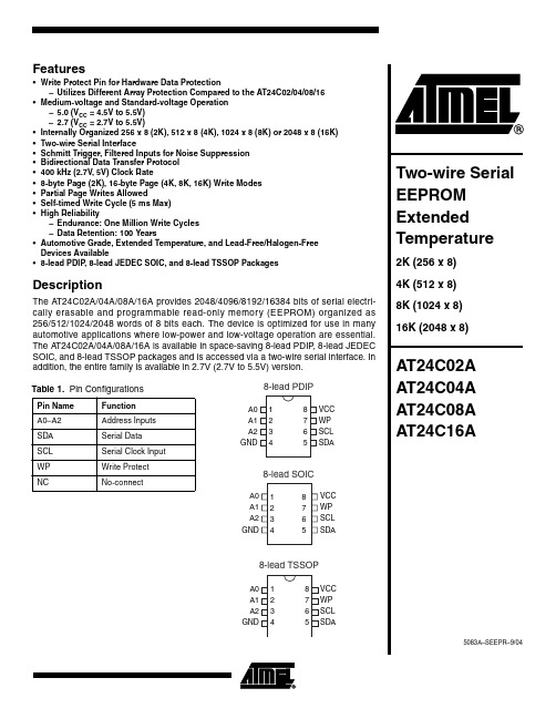
1Features•Write Protect Pin for Hardware Data Protection –Utilizes Different Array Protection Compared to the AT24C02/04/08/16•Medium-voltage and Standard-voltage Operation –5.0 (V CC = 4.5V to 5.5V)–2.7 (V CC = 2.7V to 5.5V)•Internally Organized 256 x 8 (2K), 512 x 8 (4K), 1024 x 8 (8K) or 2048 x 8 (16K)•Two-wire Serial Interface•Schmitt Trigger, Filtered Inputs for Noise Suppression •Bidirectional Data Transfer Protocol •400 kHz (2.7V, 5V) Clock Rate•8-byte Page (2K), 16-byte Page (4K, 8K, 16K) Write Modes •Partial Page Writes Allowed•Self-timed Write Cycle (5 ms Max)•High Reliability–Endurance: One Million Write Cycles –Data Retention: 100 Years•Automotive Grade, Extended Temperature, and Lead-Free/Halogen-Free Devices Available•8-lead PDIP , 8-lead JEDEC SOIC, and 8-lead TSSOP PackagesDescriptionThe AT24C02A/04A/08A/16A provides 2048/4096/8192/16384 bits of serial electri-cally erasable and programmable read-only memory (EEPROM) organized as 256/512/1024/2048 words of 8 bits each. The device is optimized for use in many automotive applications where low-power and low-voltage operation are essential.The A T24C02A/04A/08A/16A is available in space-saving 8-lead PDIP , 8-lead JEDEC SOIC, and 8-lead TSSOP packages and is accessed via a two-wire serial interface. In addition, the entire family is available in 2.7V (2.7V to 5.5V) version.Table 1. Pin Configurations2AT24C02A/04A/08A/16A5083A–SEEPR–9/04Figure 1. Block DiagramPin DescriptionSERIAL CLOCK (SCL): The SCL input is used to positive edge clock data into each EEPROM device and negative edge clock data out of each device.SERIAL DATA (SDA): The SDA pin is bidirectional for serial data transfer. This pin is open-drain driven and may be wire-ORed with any number of other open-drain or open-collector devices.DEVICE/PAGE ADDRESSES (A2, A1, A0): The A2, A1, and A0 pins are device address inputs that must be hardwired for the AT24C02A. As many as eight 2K devices may be addressed on a single bus system. (Device addressing is discussed in detail under Device Addressing, page 9).The AT24C04A uses the A2 and A1 inputs for hardwire addressing, and a total of four 4K devices may be addressed on a single bus system. The A0 pin is a no-connect.Absolute Maximum Ratings**NOTICE:Stresses beyond those listed under “Absolute Maximum Ratings” may cause permanent dam-age to the device. This is a stress rating only and functional operation of the device at these or any other conditions beyond those indicated in the operational sections of this specification is not implied. Exposure to absolute maximum rating conditions for extended periods may affect device reliability.3AT24C02A/04A/08A/16A5083A–SEEPR–9/04The AT24C08A only uses the A2 input for hardwire addressing, and a total of two 8K devices may be addressed on a single bus system. The A0 and A1 pins are no-connects.The AT24C16A does not use the device address pins, which limits the number of devices on a single bus to one. The A0, A1, and A2 pins are no-connects.WRITE PROTECT (WP): The AT24C02A/04A/08A/16A have a WP pin that provides hardware data protection. The WP pin allows normal read/write operations when con-nected to ground (GND). When the WP pin is connected to V CC , the write protection feature is enabled and operates as shown. (See Table 1.)Table 1. Write ProtectMemory OrganizationAT24C02A, 2K SERIAL EEPROM: The 2K is internally organized with 32 pages of 8bytes each. Random word addressing requires an 8-bit data word address.AT24C04A, 4K SERIAL EEPROM: The 4K is internally organized with 32 pages of 16bytes each. Random word addressing requires a 9-bit data word address.AT24C08A, 8K SERIAL EEPROM: The 8K is internally organized with 64 pages of 16bytes each. Random word addressing requires a 10-bit data word address.AT24C16A, 16K SERIAL EEPROM: The 16K is internally organized with 128 pages of 16 bytes each. Random word addressing requires an 11-bit data word address.Note:This parameter is characterized and is not 100% tested.Table 2. Pin Capacitance4AT24C02A/04A/08A/16A5083A–SEEPR–9/04Note:1.V IL min and V IH max are reference only and are not tested.Table 3. DC CharacteristicsApplicable over recommended operating range from: T AE = −40°C to +125°C, V CC = +2.7V to +5.5V5AT24C02A/04A/08A/16A5083A–SEEPR–9/04Note:1.This parameter is characterized and is not 100% tested (T A = 25°C).2.This parameter is characterized and is not 100% tested.Table 4. AC CharacteristicsApplicable over recommended operating range from T AE = −40°C to +125°C, V CC = +2.7V to +5.5V, CL = 1 TTL Gate and 100 pF (unless otherwise noted).6AT24C02A/04A/08A/16A5083A–SEEPR–9/04Device OperationCLOCK and DATA TRANSITIONS: The SDA pin is normally pulled high with an exter-nal device. Data on the SDA pin may change only during SCL low time periods (see Figure 2). Data changes during SCL high periods will indicate a start or stop condition as defined in Figure 2.Figure 2. Data ValiditySTART CONDITION: A high-to-low transition of SDA with SCL high is a start condition that must precede any other command (see Figure 3).Figure 3. Start and Stop DefinitionSTOP CONDITION: A low-to-high transition of SDA with SCL high is a stop condition.After a read sequence, the stop command will place the EEPROM in a standby power mode (see Figure 3).ACKNOWLEDGE: All addresses and data words are serially transmitted to and from the EEPROM in 8-bit words. The EEPROM sends a “0” to acknowledge that it has received each word. This happens during the ninth clock cycle.STANDBY MODE: The AT24C02A/04A/08A/16A features a low-power standby mode that is enabled (a) upon power-up and (b) after the receipt of the STOP bit and the com-pletion of any internal operations.7AT24C02A/04A/08A/16A5083A–SEEPR–9/04MEMORY RESET: After an interruption in protocol, power loss or system reset, any two-wire part can be reset by following these steps:1.Clock up to 9 cycles.2.Look for SDA high in each cycle while SCL is high.3.Create a start condition as SDA is high.Figure 4. Bus TimingFigure 5. Write Cycle TimingNote:The write cycle time t WRis the time from a valid stop condition of a write sequence to the end of the interval clear/write cycle.8AT24C02A/04A/08A/16A5083A–SEEPR–9/04Figure 6.Output Acknowledge9AT24C02A/04A/08A/16A5083A–SEEPR–9/04Device AddressingThe 2K, 4K, and 8K EEPROM devices all require an 8-bit device address word following a start condition to enable the chip for a read or write operation, as shown in Figure 7.Figure 7. Device AddressThe device address word consists of a mandatory “1”, “0” sequence for the first four most significant bits as shown. This is common to all the EEPROM devices.The next three bits are the A2, A1, and A0 device address bits for the 2K EEPROM.These three bits must compare to their corresponding hardwired input pins.The 4K EEPROM only uses the A2 and A1 device address bits with the third bit being a memory page address bit. The two device address bits must compare to their corre-sponding hardwired input pins. The A0 pin is no-connect.The 8K EEPROM only uses the A2 device address bit with the next two bits being for memory page addressing. The A2 bit must compare to its corresponding hardwired input pin. The A1 and A0 pins are no-connect.The 16K EEPROM does not use the device address pins, which limits the number of devices on a single bus to one. The A0, A1, and A2 pins are no-connects.The eighth bit of the device address is the read/write operation select bit. A read opera-tion is initiated if this bit is high, and a write operation is initiated if this bit is low.Upon a compare of the device address, the EEPROM will output a “0”. If a compare is not made, the chip will return to a standby state.Write OperationsBYTE WRITE: A write operation requires an 8-bit data word address following the device address word and acknowledgement. Upon receipt of this address, the EEPROM will again respond with a “0” and then clock in the first 8-bit data word. Following receipt of the 8-bit data word, the EEPROM will output a “0” and the addressing device, such as a microcontroller, must terminate the write sequence with a stop condition. At this time,the EEPROM enters an internally-timed write cycle, t WR , to the nonvolatile memory. All inputs are disabled during this write cycle, and the EEPROM will not respond until the write is complete, as shown in Figure 8.10AT24C02A/04A/08A/16A5083A–SEEPR–9/04Figure 8. Byte WritePAGE WRITE: The 2K EEPROM is capable of an 8-byte page write, and the 4K, 8K,and 16K devices are capable of 16-byte page writes.A page write is initiated the same as a byte write, but the microcontroller does not send a stop condition after the first data word is clocked in. Instead, after the EEPROM acknowledges receipt of the first data word, the microcontroller can transmit up to seven (2K) or fifteen (4K, 8K, 16K) more data words. The EEPROM will respond with a “0”after each data word received. The microcontroller must terminate the page write sequence with a stop condition, as shown in Figure 9.Figure 9. Page WriteThe data word address lower three (2K) or four (4K, 8K, 16K) bits are internally incre-mented following the receipt of each data word. The higher data word address bits are not incremented, retaining the memory page row location. When the word address,internally generated, reaches the page boundary, the following byte is placed at the beginning of the same page. If more than eight (2K) or sixteen (4K, 8K, 16K) data words are transmitted to the EEPROM, the data word address will “roll over” and previous data will be overwritten.ACKNOWLEDGE POLLING: Once the internally-timed write cycle has started and the EEPROM inputs are disabled, acknowledge polling can be initiated. This involves send-ing a start condition followed by the device address word. The read/write bit is representative of the operation desired. Only if the internal write cycle has completed will the EEPROM respond with a “0” allowing the read or write sequence to continue.11AT24C02A/04A/08A/16A5083A–SEEPR–9/04Read OperationsRead operations are initiated the same way as write operations with the exception that the read/write select bit in the device address word is set to “1”. There are three read operations: current address read, random address read and sequential read.CURRENT ADDRESS READ: The internal data word address counter maintains the last address accessed during the last read or write operation, incremented by one. This address stays valid between operations as long as the chip power is maintained. The address “roll over” during read is from the last byte of the last memory page to the first byte of the first page. The address “roll over” during write is from the last byte of the cur-rent page to the first byte of the same page.Once the device address with the read/write select bit set to “1” is clocked in and acknowledged by the EEPROM, the current address data word is serially clocked out.The microcontroller does not respond with an input “0” but does generate a following stop condition, as shown in Figure 10.Figure 10. Current Address ReadRANDOM READ: A random read requires a “dummy” byte write sequence to load in the data word address. Once the device address word and data word address are clocked in and acknowledged by the EEPROM, the microcontroller must generate another start condition. The microcontroller now initiates a current address read by sending a device address with the read/write select bit high. The EEPROM acknowledges the device address and serially clocks out the data word. The microcontroller does not respond with a “0” but does generate a following stop condition, as shown in Figure 11.Figure 11. Random ReadSEQUENTIAL READ: Sequential reads are initiated by either a current address read or a random address read. After the microcontroller receives a data word, it responds with an acknowledge. As long as the EEPROM receives an acknowledge, it will continue to increment the data word address and serially clock out sequential data words. When the memory address limit is reached, the data word address will “roll over” and the sequen-tial read will continue. The sequential read operation is terminated when the12AT24C02A/04A/08A/16A5083A–SEEPR–9/04microcontroller does not respond with a “0” but does generate a following stop condition,as shown in Figure 12.Figure 12.Sequential Read13AT24C02A/04A/08A/16A5083A–SEEPR–9/04Note:For 2.7V devices used in the 4.5V to 5.5V range, please refer to performance values in the AC and DC characteristics tables (Table 3 on page 4 and Table 4 on page 5).AT24C02A Ordering Information14AT24C02A/04A/08A/16A5083A–SEEPR–9/04Note:For 2.7V devices used in the 4.5V to 5.5V range, please refer to performance values in the AC and DC characteristics tables (Table 3 on page 4 and Table 4 on page 5).AT24C04A Ordering Information15AT24C02A/04A/08A/16A5083A–SEEPR–9/04Note:For 2.7V devices used in the 4.5V to 5.5V range, please refer to performance values in the AC and DC characteristics tables (Table 3 on page 4 and Table 4 on page 5).AT24C08A Ordering Information16AT24C02A/04A/08A/16A5083A–SEEPR–9/04Note:For 2.7V devices used in the 4.5V to 5.5V range, please refer to performance values in the AC and DC characteristics table (Table 3 on page 4 and Table 4 on page 5).AT24C16A Ordering Information17AT24C02A/04A/08A/16A5083A–SEEPR–9/04Packaging Information8P3 – PDIP18AT24C02A/04A/08A/16A5083A–SEEPR–9/048S1 – JEDEC SOIC19AT24C02A/04A/08A/16A5083A–SEEPR–9/048A2 – TSSOP5083A–SEEPR–9/04Disclaimer: The information in this document is provided in connection with Atmel products. No license, express or implied, by estoppel or otherwise,to any intellectual property right is granted by this document or in connection with the sale of Atmel products. EXCEPT AS SET FORTH IN ATMEL ’S TERMS AND CONDI-TIONS OF SALE LOCATED ON ATMEL ’S WEB SITE, ATMEL ASSUMES NO LIABILITY WHATSOEVER AND DISCLAIMS ANY EXPRESS, IMPLIED OR STATUTORY WARRANTY RELATING TO ITS PRODUCTS INCLUDING, BUT NOT LIMITED TO, THE IMPLIED WARRANTY OF MERCHANTABILITY, FITNESS FOR A PARTICULAR PURPOSE, OR NON-INFRINGEMENT. IN NO EVENT SHALL ATMEL BE LIABLE FOR ANY DIRECT, INDIRECT, CONSEQUENTIAL, PUNITIVE, SPECIAL OR INCIDEN-TAL DAMAGES (INCLUDING, WITHOUT LIMITATION, DAMAGES FOR LOSS OF PROFITS, BUSINESS INTERRUPTION, OR LOSS OF INFORMATION) ARISING OUT OF THE USE OR INABILITY TO USE THIS DOCUMENT, EVEN IF ATMEL HAS BEEN ADVISED OF THE POSSIBILITY OF SUCH DAMAGES. Atmel makes no representations or warranties with respect to the accuracy or completeness of the contents of this document and reserves the right to make changes to specifications and product descriptions at any time without notice. Atmel does not make any commitment to update the information contained herein. Atmel’s products are not intended, authorized, or warranted for use as components in applications intended to support or sustain life.Atmel CorporationAtmel Operations2325 Orchard Parkway San Jose, CA 95131, USA Tel: 1(408) 441-0311Fax: 1(408) 487-2600Regional HeadquartersEuropeAtmel SarlRoute des Arsenaux 41Case Postale 80CH-1705 Fribourg SwitzerlandTel: (41) 26-426-5555Fax: (41) 26-426-5500AsiaRoom 1219Chinachem Golden Plaza 77 Mody Road Tsimshatsui East Kowloon Hong KongTel: (852) 2721-9778Fax: (852) 2722-1369Japan9F, Tonetsu Shinkawa Bldg.1-24-8 ShinkawaChuo-ku, Tokyo 104-0033JapanTel: (81) 3-3523-3551Fax: (81) 3-3523-7581Memory2325 Orchard Parkway San Jose, CA 95131, USA Tel: 1(408) 441-0311Fax: 1(408) 436-4314Microcontrollers2325 Orchard Parkway San Jose, CA 95131, USA Tel: 1(408) 441-0311Fax: 1(408) 436-4314La Chantrerie BP 7060244306 Nantes Cedex 3, France Tel: (33) 2-40-18-18-18Fax: (33) 2-40-18-19-60ASIC/ASSP/Smart CardsZone Industrielle13106 Rousset Cedex, France Tel: (33) 4-42-53-60-00Fax: (33) 4-42-53-60-011150 East Cheyenne Mtn. Blvd.Colorado Springs, CO 80906, USA Tel: 1(719) 576-3300Fax: 1(719) 540-1759Scottish Enterprise Technology Park Maxwell BuildingEast Kilbride G75 0QR, Scotland Tel: (44) 1355-803-000Fax: (44) 1355-242-743RF/AutomotiveTheresienstrasse 2Postfach 353574025 Heilbronn, Germany Tel: (49) 71-31-67-0Fax: (49) 71-31-67-23401150 East Cheyenne Mtn. Blvd.Colorado Springs, CO 80906, USA Tel: 1(719) 576-3300Fax: 1(719) 540-1759Biometrics/Imaging/Hi-Rel MPU/High Speed Converters/RF DatacomAvenue de Rochepleine BP 12338521 Saint-Egreve Cedex, France Tel: (33) 4-76-58-30-00Fax: (33) 4-76-58-34-80Literature Requests/literature© Atmel Corporation 2004. All rights reserved. Atmel ®, logo and combinations thereof are registered trademarks and Everywhere Y ou Are SM is a trademark of Atmel Corporation or its subsidiaries. Other terms and product names may be the trademarks of others.。
WB-100电子报价收BOM_201900708

SAF20171221087A
ELEC SMD -> CCSG015075002-SAM ELEC SMD -> New part
0402贴片陶瓷电容:15PF,50V,5%,COG,#CL05C150JB5NNN,ROHS,三星 贴片晶振:26MHz ±10ppm Crystal 9pF 60 Ohms SMD3225, 7U026000W109,ROHS,晶科鑫
ELEC SMD -> CCSG604016202-HXK ELEC SMD -> CCSG047581310-SAM ELEC SMD -> CCSG047175002-SAM ELEC SMD -> CCSG605026201-YAG ELEC SMD -> New part ELEC SMD -> New part ELEC SMD -> LLSG040180051-TDK ELEC SMD -> LLSG04027C050-TDK ELEC SMD -> LLSG040390050-TDK ELEC SMD -> New part ELEC SMD -> LLSG04068B050-VEN
第 2 页,共 3 页
贴片电容 集成电路
11 11
线路板 贴片电阻
LED 轻触开关
11 11 11 11
贴片电阻 贴片电容 集成电路
晶振 香港电阻 香港电阻
11 11 11 11 11 11
积层电感 积层电感 贴片电容
贴片电容
贴片电容 贴片电容 贴片电阻 贴片电阻 插件晶振 集成电路
11 11 11
035
ELEC SMD '+> CYDG03HC49000-ZCD 插件晶振:4.8660MHz,HC-49U/S,20PF,±20ppm,紫程,ROHS2.0,REACH,CP65,
- 1、下载文档前请自行甄别文档内容的完整性,平台不提供额外的编辑、内容补充、找答案等附加服务。
- 2、"仅部分预览"的文档,不可在线预览部分如存在完整性等问题,可反馈申请退款(可完整预览的文档不适用该条件!)。
- 3、如文档侵犯您的权益,请联系客服反馈,我们会尽快为您处理(人工客服工作时间:9:00-18:30)。
物料编号CC0402CRNPO9BN2R7细参数_易容网
MLCC即是多层陶瓷电容片式,是电子信息产品不可或缺的基本组件之一。
我国MLCC的生产起步在80年代初,行业早期主要是在外资企业的带动下发展起来的,近年来国内企业在技术上实现突破,行业国产化成效显著,并推动了MLCC产量迅速增长。
目前,MLCC的应用领域已从手机、电脑、电视机等消费电子领域,逐步拓展到新能源发电、新能源汽车、节能灯具、轨道交通、直流输变电、三网融合、高清电视、机顶盒、手机电视等多个行业。
对于这个悄悄活跃在人们生活中的元件你又知道多少呢.
本次易容网为大家推荐比较常用的MLCC国巨 | Yageo品牌的料号CC0402CRNPO9BN2R7的相关参数
易容网是深圳市易容信息技术有限公司独自研发的全球最大的MLCC搜索采购服务网站,2014年创立于深圳市南山区,全国首家电子元器件行业电容元件的搜索引擎及o2o商务服务平台。
易容网()现已建成全球最大的MLCC电容搜索引擎数据库,包含全球25家电容生产厂商超过28万组MLCC产品数据,用户可根据行业应用、物料编号、规格参数等信息快速的找到所有相关的MLCC电容数据。
易容网在搜索服务的前提下还提供村田、TDK、国巨、太阳诱电、风华高科等常见品牌产品的o2o商务服务,让企业客户实现询价、报价、在线订单、出库、实时物流、签收、账期服务等在线一站式商务服务体验。