AT28LV010-20JU;AT28LV010-20TU;中文规格书,Datasheet资料
ATTINY28L-4PC,ATTINY28L-4PI,ATTINY28L-4AC,ATTINY28L-4AU,ATTINY28L-4AI,规格书,Datasheet 资料
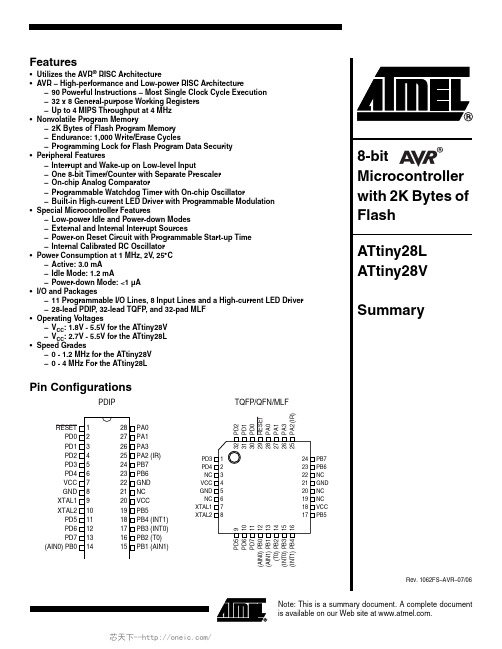
1Features•Utilizes the AVR ® RISC Architecture•AVR – High-performance and Low-power RISC Architecture–90 Powerful Instructions – Most Single Clock Cycle Execution –32 x 8 General-purpose Working Registers –Up to 4 MIPS Throughput at 4 MHz •Nonvolatile Program Memory–2K Bytes of Flash Program Memory –Endurance: 1,000 Write/Erase Cycles–Programming Lock for Flash Program Data Security •Peripheral Features–Interrupt and Wake-up on Low-level Input–One 8-bit Timer/Counter with Separate Prescaler –On-chip Analog Comparator–Programmable Watchdog Timer with On-chip Oscillator–Built-in High-current LED Driver with Programmable Modulation •Special Microcontroller Features–Low-power Idle and Power-down Modes –External and Internal Interrupt Sources–Power-on Reset Circuit with Programmable Start-up Time –Internal Calibrated RC Oscillator •Power Consumption at 1 MHz, 2V , 25°C –Active: 3.0 mA –Idle Mode: 1.2 mA–Power-down Mode: <1 µA •I/O and Packages–11 Programmable I/O Lines, 8 Input Lines and a High-current LED Driver –28-lead PDIP , 32-lead TQFP , and 32-pad MLF •Operating Voltages–V CC : 1.8V - 5.5V for the ATtiny28V –V CC : 2.7V - 5.5V for the ATtiny28L •Speed Grades–0 - 1.2 MHz for the ATtiny28V –0 - 4 MHz For the ATtiny28LPin ConfigurationsPDIPTQFP/QFN/MLF8-bit Microcontroller with 2K Bytes of ATtiny28L ATtiny28V SummaryNote: This is a summary document. A complete documentis available on our Web site at .2ATtiny28L/V1062FS–AVR–07/06DescriptionThe ATtiny28 is a low-power CMOS 8-bit microcontroller based on the AVR RISC archi-tecture. By executing powerful instructions in a single clock cycle, the ATtiny28 achieves throughputs approaching 1 MIPS per MHz, allowing the system designer to optimize power consumption versus processing speed. The AVR core combines a rich instruction set with 32 general-purpose working registers. All the 32 registers are directly con-nected to the Arithmetic Logic Unit (ALU), allowing two independent registers to be accessed in one single instruction executed in one clock cycle. The resulting architec-ture is more code efficient while achieving throughputs up to ten times faster than conventional CISC microcontrollers.Block DiagramFigure 1. The ATtiny28 Block DiagramThe ATtiny28 provides the following features: 2K bytes of Flash, 11 general-purpose I/O lines, 8 input lines, a high-current LED driver, 32 general-purpose working registers, an 8-bit timer/counter, internal and external interrupts, programmable Watchdog Timer with internal oscillator and 2 software-selectable power-saving modes. The Idle Mode stops the CPU while allowing the timer/counter and interrupt system to continue functioning.The Power-down mode saves the register contents but freezes the oscillator, disabling all other chip functions until the next interrupt or hardware reset. The wake-up or inter-3ATtiny28L/V1062FS–AVR–07/06rupt on low-level input feature enables the ATtiny28 to be highly responsive to external events, still featuring the lowest power consumption while in the power-down modes.The device is manufactured using Atmel’s high-density, nonvolatile memory technology.By combining an enhanced RISC 8-bit CPU with Flash on a monolithic chip, the Atmel ATtiny28 is a powerful microcontroller that provides a highly flexible and cost-effective solution to many embedded control applications. The ATtiny28 AVR is supported with a full suite of program and system development tools including: macro assemblers, pro-gram debugger/simulators, in-circuit emulators and evaluation kits.Pin DescriptionsVCC Supply voltage pin.GNDGround pin.Port A (PA3..PA0)Port A is a 4-bit I/O port. PA2 is output-only and can be used as a high-current LED driver. At V CC = 2.0V, the PA2 output buffer can sink 25 mA. PA3, PA1 and PA0 are bi-directional I/O pins with internal pull-ups (selected for each bit). The port pins are tri-stated when a reset condition becomes active, even if the clock is not running.Port B (PB7..PB0)Port B is an 8-bit input port with internal pull-ups (selected for all Port B pins). Port B pins that are externally pulled low will source current if the pull-ups are activated.Port B also serves the functions of various special features of the ATtiny28 as listed on page 27. If any of the special features are enabled, the pull-up(s) on the corresponding pin(s) is automatically disabled. The port pins are tri-stated when a reset condition becomes active, even if the clock is not running.Port D (PD7..PD0)Port D is an 8-bit I/O port. Port pins can provide internal pull-up resistors (selected for each bit). The port pins are tri-stated when a reset condition becomes active, even if the clock is not running.XTAL1Input to the inverting oscillator amplifier and input to the internal clock operating circuit.XTAL2Output from the inverting oscillator amplifier.pulses longer than 50 ns will generate a reset, even if the clock is not running. Shorter pulses are not guaranteed to generate a reset.4ATtiny28L/V1062FS–AVR–07/06Notes:1.For compatibility with future devices, reserved bits should be written to zero if accessed. Reserved I/O memory addressesshould never be written.2.Some of the status flags are cleared by writing a logical “1” to them. Note that the CBI and SBI instructions will operate on allbits in the I/O register, writing a one back into any flag read as set, thus clearing the flag. The CBI and SBI instructions work with registers $00 to $1F only.Register SummaryAddressNameBit 7Bit 6Bit 5Bit 4Bit 3Bit 2Bit 1Bit 0Page$3F SREG ITHSVNZCpage 6$3E Reserved ...Reserved $20Reserved $1F Reserved $1E Reserved $1D Reserved $1C Reserved $1B PORTA ----PORTA3PORTA2PORTA1PORTA0page 32$1A PACR ----DDA3PA2HCDDA1DDA0page 32$19PINA ----PINA3-PINA1PINA0page 32$18Reserved $17Reserved $16PINB PINB7PINB6PINB5PINB4PINB3PINB2PINB1PINB0page 32$15Reserved $14Reserved $13Reserved $12PORTD PORTD7PORTD6PORTD5PORTD4PORTD3PORTD2PORTD1PORTD0page 33$11DDRD DDD7DDD6DDD5DDD4DDD3DDD2DDD1DDD0page 33$10PIND PIND7PIND6PIND5PIND4PIND3PIND2PIND1PIND0page 33$0F Reserved $0E Reserved $0D Reserved $0C Reserved $0B Reserved $0A Reserved $09Reserved $08ACSR ACD -ACO ACI ACIE -ACIS1ACIS0page 44$07MCUCS PLUPB -SE SM WDRF -EXTRF PORF page 19$06ICR INT1INT0LLIE TOIE0ISC11ISC10ISC01ISC00page 22$05IFR INTF1INTF0-TOV0----page 23$04TCCR0FOV0--OOM01OOM00CS02CS01CS00page 35$03TCNT0Timer/Counter0 (8-bit)page 36$02MODCR ONTIM4ONTIM3ONTIM2ONTIM1 ONTIM0MCONF2MCONF1MCONF0page 43$01WDTCR ---WDTOEWDEWDP2WDP1WDP0page 37$00OSCCALOscillator Calibration Registerpage 95ATtiny28L/V1062FS–AVR–07/06Instruction Set SummaryMnemonicOperandsDescriptionOperationFlags# ClocksARITHMETIC AND LOGIC INSTRUCTIONSADD Rd, Rr Add Two RegistersRd ← Rd + Rr Z,C,N,V,H 1ADC Rd, Rr Add with Carry Two Registers Rd ← Rd + Rr + C Z,C,N,V,H 1SUB Rd, Rr Subtract Two Registers Rd ← Rd - Rr Z,C,N,V,H 1SUBI Rd, K Subtract Constant from Register Rd ← Rd - K Z,C,N,V,H 1SBC Rd, Rr Subtract with Carry Two Registers Rd ← Rd - Rr - C Z,C,N,V,H 1SBCI Rd, K Subtract with Carry Constant from Reg.Rd ← Rd - K - C Z,C,N,V,H 1AND Rd, Rr Logical AND RegistersRd ← Rd • Rr Z,N,V 1ANDI Rd, K Logical AND Register and Constant Rd ← Rd • K Z,N,V 1OR Rd, Rr Logical OR RegistersRd ← Rd v Rr Z,N,V 1ORI Rd, K Logical OR Register and Constant Rd ← Rd v K Z,N,V 1EOR Rd, Rr Exclusive OR Registers Rd ← Rd ⊕ Rr Z,N,V 1COM Rd One’s Complement Rd ← $FF - Rd Z,C,N,V 1NEG Rd Two’s Complement Rd ← $00 - Rd Z,C,N,V,H 1SBR Rd, K Set Bit(s) in Register Rd ← Rd v K Z,N,V 1CBR Rd, K Clear Bit(s) in Register Rd ← Rd • (FFh - K)Z,N,V 1INC Rd Increment Rd ← Rd + 1Z,N,V 1DEC Rd DecrementRd ← Rd - 1 Z,N,V 1TST Rd Test for Zero or Minus Rd ← Rd • Rd Z,N,V1CLR Rd Clear Register Rd ← Rd ⊕ Rd Z,N,V 1SER Rd Set Register Rd ← $FF None 1BRANCH INSTRUCTIONSRJMP k Relative JumpPC ← PC + k + 1None 2RCALL kRelative Subroutine Call PC ← PC + k + 1None 3RET Subroutine Return PC ← STACK None 4RETI Interrupt Return PC ← STACKI 4CPSE Rd, Rr Compare, Skip if Equal if (Rd = Rr) PC ← PC + 2 or 3None 1/2CP Rd, Rr CompareRd - Rr Z,N,V,C,H 1CPC Rd, Rr Compare with CarryRd - Rr - C Z,N,V,C,H 1CPI Rd, K Compare Register with Immediate Rd - KZ N,V,C,H 1SBRC Rr, b Skip if Bit in Register Cleared if (Rr(b) = 0) PC ← PC + 2 or 3None 1/2SBRS Rr, b Skip if Bit in Register is Set if (Rr(b) = 1) PC ← PC + 2 or 3None 1/2SBIC P, b Skip if Bit in I/O Register Cleared if (P(b) = 0) PC ← PC + 2 or 3None 1/2SBIS P, b Skip if Bit in I/O Register is Set if (P(b) = 1) PC ← PC + 2 or 3None 1/2BRBS s, k Branch if Status Flag Set if (SREG(s) = 1) then PC ← PC + k + 1None 1/2BRBC s, k Branch if Status Flag Cleared if (SREG(s) = 0) then PC ← PC + k + 1None 1/2BREQ k Branch if Equal if (Z = 1) then PC ← PC + k + 1None 1/2BRNE k Branch if Not Equal if (Z = 0) then PC ← PC + k + 1None 1/2BRCS k Branch if Carry Set if (C = 1) then PC ← PC + k + 1None 1/2BRCC k Branch if Carry Cleared if (C = 0) then PC ← PC + k + 1None 1/2BRSH k Branch if Same or Higher if (C = 0) then PC ← PC + k + 1None 1/2BRLO k Branch if Lower if (C = 1) then PC ← PC + k + 1None 1/2BRMI k Branch if Minus if (N = 1) then PC ← PC + k + 1None 1/2BRPL k Branch if Plusif (N = 0) then PC ← PC + k + 1None 1/2BRGE k Branch if Greater or Equal, Signed if (N ⊕ V = 0) then PC ← PC + k + 1None 1/2BRLT k Branch if Less than Zero, Signed if (N ⊕ V = 1) then PC ← PC + k + 1None 1/2BRHS k Branch if Half-carry Flag Set if (H = 1) then PC ← PC + k + 1None 1/2BRHC k Branch if Half-carry Flag Cleared if (H = 0) then PC ← PC + k + 1None 1/2BRTS k Branch if T-flag Set if (T = 1) then PC ← PC + k + 1None 1/2BRTC k Branch if T-flag Cleared if (T = 0) then PC ← PC + k + 1None 1/2BRVS k Branch if Overflow Flag is Set if (V = 1) then PC ← PC + k + 1None 1/2BRVC k Branch if Overflow Flag is Cleared if (V = 0) then PC ← PC + k + 1None 1/2BRIE k Branch if Interrupt Enabled if (I = 1) then PC ← PC + k + 1None 1/2BRIDkBranch if Interrupt Disabledif (I = 0) then PC ← PC + k + 1None1/26ATtiny28L/V1062FS–AVR–07/06DATA TRANSFER INSTRUCTIONSLD Rd, Z Load Register Indirect Rd ← (Z)None 2ST Z, Rr Store Register Indirect (Z) ← Rr None 2MOV Rd, Rr Move between Registers Rd ← Rr None 1LDI Rd, K Load Immediate Rd ←K None 1IN Rd, P In Port Rd ← P None 1OUT P, RrOut PortP ← Rr None 1LPMLoad Program MemoryR0 ← (Z)None3BIT AND BIT-TEST INSTRUCTIONS SBI P, b Set Bit in I/O Register I/O(P,b) ← 1None 2CBI P, b Clear Bit in I/O Register I/O(P,b) ←None 2LSL Rd Logical Shift LeftRd(n+1) ← Rd(n), Rd(0) ← 0Z,C,N,V 1LSR Rd Logical Shift Right Rd(n) ← Rd(n+1), Rd(7) ← 0Z,C,N,V 1ROL Rd Rotate Left through Carry Rd(0) ← C, Rd(n+1) ← Rd(n), C ← Rd(7)Z,C,N,V 1ROR Rd Rotate Right through Carry Rd(7) ← C, Rd(n) ← Rd(n+1), C ← Rd(0)Z,C,N,V 1ASR Rd Arithmetic Shift Right Rd(n) ← Rd(n+1), n = 0..6Z,C,N,V 1SWAP Rd Swap Nibbles Rd(3..0) ← Rd(7..4), Rd(7..4) ← Rd(3..0)None 1BSET s Flag Set SREG(s) ← 1SREG(s)1BCLR s Flag Clear SREG(s) ← 0SREG(s)1BST Rr, b Bit Store from Register to T T ← Rr(b)T 1BLD Rd, bBit Load from T to Register Rd(b) ← T None 1SEC Set Carry C ← 1C 1CLC Clear Carry C ←0C 1SEN Set Negative Flag N ← 1N 1CLN Clear Negative Flag N ← 0N 1SEZ Set Zero Flag Z ←1Z 1CLZ Clear Zero Flag Z ← 0Z1SEI Global Interrupt Enable I ← 1I 1CLI Global Interrupt Disable I ←I 1SES Set Signed Test FlagS ← 1S 1CLS Clear Signed Test Flag S ←0S 1SEV Set Two’s Complement OverflowV ←1V 1CLV Clear Two’s Complement Overflow V ← 0V 1SET Set T in SREG T ← 1T 1CLT Clear T in SREG T ← 0T 1SEH Set Half-carry Flag in SREG H ← 1H 1CLH Clear Half-carry Flag in SREG H ←H 1NOP No Operation None 1SLEEP Sleep(see specific descr. for Sleep function)None 1WDRWatchdog Reset(see specific descr. for WDR/timer)None1Instruction Set Summary (Continued)MnemonicOperandsDescriptionOperationFlags# Clocks7ATtiny28L/V1062FS–AVR–07/06Notes:1.This device can also be supplied in wafer form. Please contact your local Atmel sales office for detailed ordering informationand minimum quantities.2.Pb-free packaging alternative, complies to the European Directive for Restriction of Hazardous Substances (RoHS direc-tive).Also Halide free and fully Green.Ordering InformationSpeed (MHz)Power Supply (Volts)Ordering Code Package (1)Operation Range 42.7 - 5.5A Ttiny28L-4AC A Ttiny28L-4PC A Ttiny28L-4MC32A 28P332M1-A Commercial (0°C to 70°C)A Ttiny28L-4AI A Ttiny28L-4AU (2)A Ttiny28L-4PI A Ttiny28L-4PU (2)A Ttiny28L-4MI A Ttiny28L-4MU (2)32A 32A 28P328P332M1-A 32M1-A Industrial (-40°C to 85°C)1.21.8 - 5.5A Ttiny28V-1AC A Ttiny28V-1PC A Ttiny28V-1MC32A 28P332M1-A Commercial (0°C to 70°C)A Ttiny28V-1AI A Ttiny28V-1AU (2)A Ttiny28V-1PI A Ttiny28V-1PU (2)A Ttiny28V-1MI A Ttiny28V-1MU (2)32A 32A 28P328P332M1-A 32M1-AIndustrial (-40°C to 85°C)Package Type32A 32-lead, Thin (1.0 mm) Plastic Quad Flat Package (TQFP)28P328-lead, 0.300" Wide, Plastic Dual Inline Package (PDIP)32M1-A32-pad, 5x5x1.0 body, Lead Pitch 0.50mm, Quad Flat No-lead/Micro Lead Frame Package (QFN/MLF)8ATtiny28L/V1062FS–AVR–07/06Packaging Information32A9ATtiny28L/V1062FS–AVR–07/0628P310ATtiny28L/V1062FS–AVR–07/0632M1-A11ATtiny28L/V1062FS–AVR–07/06ErrataAll revisionsNo known errata.12ATtiny28L/V1062FS–AVR–07/06Datasheet Revision HistoryPlease note that the referring page numbers in this section are referred to this docu-ment. The referring revision in this section are referring to the document revision.Rev – 01/06G 1.Updated chapter layout.2.Updated “Ordering Information” on page 7.Rev – 01/06G1.Updated description for “Port A” on page 25.2.Added note 6 in “DC Characteristics” on page 54.3.Updated “Ordering Information” on page 7.4.Added “Errata” on page 11.Rev – 03/05F1.Updated “Electrical Characteristics” on page 54.2.MLF-package alternative changed to “Quad Flat No-Lead/Micro Lead Frame PackageQFN/MLF”.3.Updated “Ordering Information” on page 7.1062FS–AVR–07/06© 2006 Atmel Corporation . All rights reserved. ATMEL ®, logo and combinations thereof, Everywhere You Are ®, AVR ®, AVR Studio ®, and oth-ers, are registered trademarks or trademarks of Atmel Corporation or its subsidiaries. Other terms and product names may be trademarks of oth-ers.Disclaimer: The information in this document is provided in connection with Atmel products. No license, express or implied, by estoppel or otherwise,to any intellectual property right is granted by this document or in connection with the sale of Atmel products. EXCEPT AS SET FORTH IN ATMEL’S TERMS AND CONDI-TIONS OF SALE LOCATED ON ATMEL’S WEB SITE, ATMEL ASSUMES NO LIABILITY WHATSOEVER AND DISCLAIMS ANY EXPRESS, IMPLIED OR STATUTORY WARRANTY RELATING TO ITS PRODUCTS INCLUDING, BUT NOT LIMITED TO, THE IMPLIED WARRANTY OF MERCHANTABILITY, FITNESS FOR A PARTICULAR PURPOSE, OR NON-INFRINGEMENT. IN NO EVENT SHALL ATMEL BE LIABLE FOR ANY DIRECT, INDIRECT, CONSEQUENTIAL, PUNITIVE, SPECIAL OR INCIDEN-TAL DAMAGES (INCLUDING, WITHOUT LIMITATION, DAMAGES FOR LOSS OF PROFITS, BUSINESS INTERRUPTION, OR LOSS OF INFORMATION) ARISING OUT OF THE USE OR INABIL ITY TO USE THIS DOCUMENT, EVEN IF ATMEL HAS BEEN ADVISED OF THE POSSIBIL ITY OF SUCH DAMAGES. Atmel makes no representations or warranties with respect to the accuracy or completeness of the contents of this document and reserves the right to make changes to specifications and product descriptions at any time without notice. Atmel does not make any commitment to update the information contained herein. Unless specifically provided otherwise, Atmel products are not suitable for, and shall not be used in, automotive applications. Atmel’s products are not intended, authorized, or warranted for use as components in applications intended to support or sustain life.Atmel CorporationAtmel Operations2325 Orchard Parkway San Jose, CA 95131, USA Tel: 1(408) 441-0311Fax: 1(408) 487-2600Regional HeadquartersEuropeAtmel SarlRoute des Arsenaux 41Case Postale 80CH-1705 Fribourg SwitzerlandTel: (41) 26-426-5555Fax: (41) 26-426-5500AsiaRoom 1219Chinachem Golden Plaza 77 Mody Road Tsimshatsui East Kowloon Hong KongTel: (852) 2721-9778Fax: (852) 2722-1369Japan9F, Tonetsu Shinkawa Bldg.1-24-8 ShinkawaChuo-ku, Tokyo 104-0033JapanTel: (81) 3-3523-3551Fax: (81) 3-3523-7581Memory2325 Orchard Parkway San Jose, CA 95131, USA Tel: 1(408) 441-0311Fax: 1(408) 436-4314Microcontrollers2325 Orchard Parkway San Jose, CA 95131, USA Tel: 1(408) 441-0311Fax: 1(408) 436-4314La Chantrerie BP 7060244306 Nantes Cedex 3, France Tel: (33) 2-40-18-18-18Fax: (33) 2-40-18-19-60ASIC/ASSP/Smart CardsZone Industrielle13106 Rousset Cedex, France Tel: (33) 4-42-53-60-00Fax: (33) 4-42-53-60-011150 East Cheyenne Mtn. Blvd.Colorado Springs, CO 80906, USA Tel: 1(719) 576-3300Fax: 1(719) 540-1759Scottish Enterprise Technology Park Maxwell BuildingEast Kilbride G75 0QR, Scotland Tel: (44) 1355-803-000Fax: (44) 1355-242-743RF/AutomotiveTheresienstrasse 2Postfach 353574025 Heilbronn, Germany Tel: (49) 71-31-67-0Fax: (49) 71-31-67-23401150 East Cheyenne Mtn. Blvd.Colorado Springs, CO 80906, USA Tel: 1(719) 576-3300Fax: 1(719) 540-1759Biometrics/Imaging/Hi-Rel MPU/High Speed Converters/RF DatacomAvenue de Rochepleine BP 12338521 Saint-Egreve Cedex, France Tel: (33) 4-76-58-30-00Fax: (33) 4-76-58-34-80Literature Requests/literature。
CAT28LV256G25;CAT28LV256G-25T;CAT28LV256GI25;CAT28LV256GI-25T;中文规格书,Datasheet资料

s CMOS and TTL Compatible I/O s Automatic Page Write Operation:– 1 to 64 Bytes in 10ms – Page Load Timers End of Write Detection:– Toggle Bit – DATA Pollings Hardware and Software Write Protection s 100,000 Program/Erase Cycles s 100 Year Data RetentionFEATURESs 3.0V to 3.6V Supplys Read Access Times: 200/250/300 ns s Low Power CMOS Dissipation:– Active: 15 mA Max.– Standby: 150 µA Max.s Simple Write Operation:– On-Chip Address and Data Latches – Self-Timed Write Cycle with Auto-Clears Fast Write Cycle Time:– 10ms Max.s Commercial, Industrial and AutomotiveTemperature RangesDESCRIPTIONThe CAT28LV256 is a fast, low power, low voltage CMOS Parallel E 2PROM organized as 32K x 8-bits. It requires a simple interface for in-system programming.On-chip address and data latches, self-timed write cycle with auto-clear and V CC power up/down write protection eliminate additional timing and protection hardware.DATA Polling and Toggle status bits signal the start and end of the self-timed write cycle. Additionally, the CAT28LV256 features hardware and software write protection.The CAT28LV256 is manufactured using Catalyst’s advanced CMOS floating gate technology. It is designed to endure 100,000 program/erase cycles and has a data retention of 100 years. The device is available in JEDEC–approved 28-pin DIP, 28-pin TSOP or 32-pin PLCC packages.BLOCK DIAGRAMA 6A 256K-Bit CMOS PARALLEL EEPROMCAT28LV256CAT28LV256PLCC Package (N, G)DIP Package (P, L)PIN CONFIGURATIONTSOP Top View (8mm X 13.4mm) (H)1234567891011121314282726252423222120191817I/O 6I/O 5I/O 4GND I/O 2A 1A 2V CC WE A 8A 9A 11OE A 7A 6A 5A 4A 3A 10I/O 7A 121615I/O 3I/O 1I/O 0A 0A 13A 14I/O 2V SSI/O 6I/O 5A 1A 0I/O 0I/O 1OE A 10CE I/O 7A 5A 4A 3A 2A 14A 12A 7A 6A 9A 11V CC WE A 13A 8A 6A 5A 4A 35678A 2A 1A 0NC 9101112I/O 013A 8A 9A 11NC 29282726OE A 10CE 25242322I/O 721I /O 1I /O 2V S SN CI /O 3I /O 4I /O 5141516171819204321323130A 7A 12A 14N C V C C W EA 13I/O 4I/O 3I/O 6TOP VIEWPIN FUNCTIONSPin Name Function Pin Name Function A 0–A 14Address Inputs WE Write Enable I/O 0–I/O 7Data Inputs/Outputs V CC 3.0 to 3.6 V Supply CE Chip Enable V SS Ground OEOutput EnableNCNo ConnectCAT28LV256CAPACITANCE T A = 25°C, f = 1.0 MHzSymbol TestMax.Units Conditions C I/O (1)Input/Output Capacitance 10pF V I/O = 0V C IN (1)Input Capacitance6pFV IN = 0VNote:(1)This parameter is tested initially and after a design or process change that affects the parameter.(2)The minimum DC input voltage is –0.5V. During transitions, inputs may undershoot to –2.0V for periods of less than 20 ns. Maximum DCvoltage on output pins is V CC +0.5V, which may overshoot to V CC +2.0V for periods of less than 20 ns.(3)Output shorted for no more than one second. No more than one output shorted at a time.(4)Latch-up protection is provided for stresses up to 100mA on address and data pins from –1V to V CC +1V.*COMMENTStresses above those listed under “Absolute Maximum Ratings” may cause permanent damage to the device.These are stress ratings only, and functional operation of the device at these or any other conditions outside of those listed in the operational sections of this specifica-tion is not implied. Exposure to any absolute maximum rating for extended periods may affect device perfor-mance and reliability.ABSOLUTE MAXIMUM RATINGS*Temperature Under Bias .................–55°C to +125°C Storage Temperature.......................–65°C to +150°C Voltage on Any Pin withRespect to Ground (2)...........–2.0V to +V CC + 2.0V V CC with Respect to Ground ...............–2.0V to +7.0V Package Power DissipationCapability (Ta = 25°C)...................................1.0W Lead Soldering Temperature (10 secs)............300°C Output Short Circuit Current (3)........................100 mA RELIABILITY CHARACTERISTICS Symbol Parameter Min.Max.Units Test MethodN END (1)Endurance 100,000Cycles/Byte MIL-STD-883, Test Method 1033T DR (1)Data Retention 100Years MIL-STD-883, Test Method 1008V ZAP (1)ESD Susceptibility 2000Volts MIL-STD-883, Test Method 3015I LTH (1)(4)Latch-Up100mAJEDEC Standard 17MODE SELECTIONModeCE WE OE I/O Power ReadL HL D OUT ACTIVE Byte Write (WE Controlled)LH D IN ACTIVE Byte Write (CE Controlled)L H D IN ACTIVE Standby, and Write Inhibit H X X High-Z STANDBY Read and Write InhibitX H HHigh-ZACTIVECAT28LV256D.C. OPERATING CHARACTERISTICSV CC = 3.0V to 3.6V, unless otherwise specifiedNote:(1)This parameter is tested initially and after a design or process change that affects the parameter.(2)V IHC = V CC –0.3V to V CC +0.3V.(3)Output floating (High-Z) is defined as the state when the external data line is no longer driven by the output buffer.CAT28LV256A.C. CHARACTERISTICS, Write Cycle V CC = 3.0V to 3.6V, unless otherwise specified28LV256-2028LV256-2528LV256-30Symbol Parameter Min.Max.Min.Max.Min.Max.Units t WC Write Cycle Time 101010ms t AS Address Setup Time 000ns t AH Address Hold Time 100100100ns t CS CE Setup Time 000ns t CH CE Hold Time 000ns t CW (3)CE Pulse Time 150150150ns t OES OE Setup Time 000ns t OEH OE Hold Time 000ns t WP (3)WE Pulse Width 150150150ns t DS Data Setup Time 505050ns t DH Data Hold Time000ns t INIT (1)Write Inhibit Period After Power-up 510510510ms t BLC (1)(4)Byte Load Cycle Time0.151000.151000.15100µsC L INCLUDES JIG CAPACITANCEINPUT PULSE LEVELSREFERENCE POINTS2.0 V0.6 VV CC - 0.3V0.0 VFigure 1. A.C. Testing Input/Output Waveform (2)28LV256 F04Note:(1)This parameter is tested initially and after a design or process change that affects the parameter.(2)Input rise and fall times (10% and 90%) < 10 ns.(3)A write pulse of less than 20ns duration will not initiate a write cycle.(4)A timer of duration t BLC max. begins with every LOW to HIGH transition of WE . If allowed to time out, a page or byte write will begin;however a transition from HIGH to LOW within t BLC max. stops the timer.Figure 2. A.C. Testing Load Circuit (example)28LV256 F05CAT28LV256ADDRESSCEOEWEDATA OUTDATA INDEVICE OPERATIONReadData stored in the CAT28LV256 is transferred to the data bus when WE is held high, and both OE and CE are held low. The data bus is set to a high impedance state when either CE or OE goes high. This 2-line control architecture can be used to eliminate bus contention in a system environment.Byte WriteA write cycle is executed when both CE and WE are low,and OE is high. Write cycles can be initiated using either WE or CE , with the address input being latched on the falling edge of WE or CE , whichever occurs last. Data,conversely, is latched on the rising edge of WE or CE ,whichever occurs first. Once initiated, a byte write cycle automatically erases the addressed byte and the new data is written within 10 ms.Figure 3. Read Cycle28LV256 F0628LV256 F07CAT28LV256ADDRESSCEOEWEDATA OUTDATA INPage WriteThe page write mode of the CAT28LV256 (essentially an extended BYTE WRITE mode) allows from 1 to 64bytes of data to be programmed within a single E 2PROM write cycle. This effectively reduces the byte-write time by a factor of 64.Following an initial WRITE operation (WE pulsed low, for t WP , and then high) the page write mode can begin by issuing sequential WE pulses, which load the address and data bytes into a 64 byte temporary buffer. The page address where data is to be written, specified by bits A 6to A 14, is latched on the last falling edge of WE . Each byte within the page is defined by address bits A 0 to A 5(which can be loaded in any order) during the first and subsequent write cycles. Each successive byte load cycle must begin within t BLC MAX of the rising edge of the preceding WE pulse. There is no page write window limitation as long as WE is pulsed low within t BLC MAX .Upon completion of the page write sequence, WE must stay high a minimum of t BLC MAX for the internal auto-matic program cycle to commence. This programming cycle consists of an erase cycle, which erases any data that existed in each addressed cell, and a write cycle,which writes new data back into the cell. A page write will only write data to the locations that were addressed and will not rewrite the entire page.28LV256 F09CAT28LV256WECEOEI/O 6DATA PollingDATA polling is provided to indicate the completion of write cycle. Once a byte write or page write cycle is initiated, attempting to read the last byte written will output the complement of that data on I/O 7 (I/O 0–I/O 6are indeterminate) until the programming cycle is com-plete. Upon completion of the self-timed write cycle, all I/O’s will output true data during a read cycle.Toggle BitIn addition to the DATA Polling feature, the device can determine the completion of a write cycle, while a write cycle is in progress, by reading data from the device.This results in I/O 6 toggling between one and zero. Once the write is complete, however, I/O 6 stops toggling and valid data can be read from the device.Figure 7. DATA Polling28LV256 F10Figure 8. Toggle Bit28LV256 F11Note:(1)Beginning and ending state of I/O 6 is indeterminate.CAT28LV256SOFTWARE DATAPROTECTION ACTIVATED(1)(4)Noise pulses of less than 20 ns on the WE or CEinputs will not result in a write cycle.SOFTWARE DATA PROTECTIONThe CAT28LV256 features a software controlled data protection scheme which, once enabled, requires a data algorithm to be issued to the device before a write can be performed. The device is shipped from Catalyst with the software protection NOT ENABLED (the CAT28LV256is in the standard operating mode).Figure 9.Write Sequence for Activating SoftwareData ProtectionFigure 10.Write Sequence for DeactivatingSoftware Data Protection28LV256 F1228LV256 F13Note:(1)Write protection is activated at this point whether or not any more writes are completed. Writing to addresses must occur within t BLCMax., after SDP activation.HARDWARE DATA PROTECTIONThe following hardware data protection features are incorporated into the CAT28LV256.(1)V CC sense provides write protection when V CC fallsbelow 2.0V min.(2) A power on delay mechanism, t INIT (see AC charac-teristics), provides a 5 to 10 ms delay before a write sequence, after V CC has reached 2.4V min.(3)Write inhibit is activated by holding any one of OElow, CE high, or WE high.CAT28LV256To activate the software data protection, the device must be sent three write commands to specific addresses with specific data (Figure 9). This sequence of commands (along with subsequent writes) must adhere to the page write timing specifications (Figure 11). Once this is done,all subsequent byte or page writes to the device must be preceded by this same set of write commands. The data protection mechanism is activated until a deactivate sequence is issued, regardless of power on/off transi-tions. This gives the user added inadvertent write pro-tection on power-up in addition to the hardware protec-tion provided.To allow the user the ability to program the device with an E 2PROM programmer (or for testing purposes) there is a software command sequence for deactivating the data protection. The six step algorithm (Figure 10) will reset the internal protection circuitry, and the device will return to standard operating mode (Figure 12 provides reset timing). After the sixth byte of this reset sequence has been issued, standard byte or page writing can commence.Figure 11. Software Data Protection TimingFigure 12. Resetting Software Data Protection Timing分销商库存信息:ONSEMICAT28LV256G25CAT28LV256G-25T CAT28LV256GI25 CAT28LV256GI-25T。
ATSTK520;中文规格书,Datasheet资料

STK520 .............................................................................................. User GuideSTK520 User Guide 3Table of ContentsSection 1Introduction............................................................................................1-2Section 2Using the STK520 Top Module.............................................................2-42.1Connecting the STK520 to the STK500 Starter Kit..................................2-42.1.1Placing an AT90PWM3 on the STK520.............................................2-42.1.2Placing an AT90PWM2 on the STK520.............................................2-52.2Programming the AVR..............................................................................2-72.2.1In-System Programming....................................................................2-72.2.2High-voltage Programming................................................................2-82.3JTAGICE mkII Connector.........................................................................2-92.4STK520 Jumpers, Leds & Test Points....................................................2-112.5DALI Interface.........................................................................................2-122.6Potentiometer.........................................................................................2-13Section 3Troubleshooting Guide........................................................................3-14Section 4Technical Specifications......................................................................4-16Section 5Technical Support ...............................................................................5-17Section 6Complete Schematics .........................................................................6-20IntroductionSection 1IntroductionThe STK520 board is a top module designed to add AT90PWM family support to theSTK500 development board from Atmel Corporation.The STK520 includes connectors and hardware allowing full utilization of the new fea-tures of the AT90PWM, while the Zero Insertion Force (ZIF) socket allows easy to use ofSO24 & SO32 packages for prototyping.This user guide acts as a general getting started guide as well as a complete technicalreference for advanced users.Notice that in this guide, the word AVR is used to refer to the target component(AT90PWM2, AT90PWM3...)Figure 1-1. STK520 Top Module for STK500Introduction1.1Features STK520 is a New Member of the Successful STK500 Starter Kit Family.Supports the AT90PWM2 & AT90PWM3.DALI Hardware Interface.Supported by AVR Studio® 4.Zero Insertion Force Socket for SO24 & SO32 Packages.High Voltage Parallell Programming.Serial Programming.DALI Peripherals can be Disconnected from the Device.6 Pin Connector for On-chip Debugging using JTAG MKII Emulator.Potentiometer for the Demo Application.Quick Reference to all Switches and Jumpers in the Silk-Screen of the PCB.Using the STK520 Top Module Section 2Using the STK520 Top Module2.1Connecting the STK520 to theSTK500 Starter Kit Connect the STK520 to the STK500 expansion header 0 and 1. It is important that the top module is connected in the correct orientation as shown in Figure 2-1. The EXPAND0 written on the STK520 top module should match the EXPAND0 written beside the expansion header on the STK500 board.Figure 2-1. Connecting STK520 to the STK500 BoardNote:Connecting the STK520 with wrong orientation may damage the board.2.1.1Placing anAT90PWM3 on theSTK520The STK520 contains both a ZIF socket for a SO32 package. Care should be taken so that the device is mounted with the correct orientation. Figure 2-2 shows the location of pin1 for the ZIF socket.Using the STK520 Top ModuleFigure 2-2. Pin1 on ZIF SocketCaution: Do not mount an AT90PWM3 on the STK520 at the same time as an AVR ismounted on the STK500 board or at the same time as an AT90PWM2 is mounted on theSTK520 board. None of the devices might work as intended.2.1.2Placing anAT90PWM2 on theSTK520The STK520 contains both a ZIF socket for a SO24 package. Care should be taken so that the device is mounted with the correct orientation. Figure 2-2 shows the location of pin1 for the ZIF socket.Figure 2-3. Pin1 on ZIF SocketPIN1PIN1Using the STK520 Top Module Caution: Do not mount an AT90PWM2 on the STK520 at the same time as an AVR is mounted on the STK500 board or at the same time as an AT90PWM3 is mounted on the STK520 board. None of the devices might work as intended.Using the STK520 Top Module2.2Programming theAVR The AVR (AT90PWM2, AT90PWM3...) can be programmed using both SPI and High-voltage Parallel Programming. This section will explain how to connect the programming cables to successfully use one of these two modes. The AVR Studio STK500 software is used in the same way as for other AVR partsNote:The AT90PWM3 also support Self Programming, See AVR109 application note for more information on this topic.2.2.1In-SystemProgramming Figure 2-4. In-System ProgrammingTo program the AT90PWM3 using ISP Programming mode, connect the 6-wire cable between the ISP6PIN connector on the STK500 board and the ISP connector on the STK520 board as shown in Figure 2-4. The device can be programmed using the Serial Programming mode in the AVR Studio4 STK500 software.Note:See STK500 User Guide for information on how to use the STK500 front-end software for ISP Programming.Using the STK520 Top Module2.2.2High-voltageProgramming Figure 2-5. High-voltage (Parallel) ProgrammingTo program the AVR using High-voltage (Parallel) Programming, connect the PROGC-TRL to PORTD and PROGDATA to PORTB on the STK500 as shown in Figure 2-5. Make sure that the TOSC-switch is placed in the XTAL position.As described in the STK500 User Guide (jumper settings), mount the BSEL2 jumper in order to High-voltage Program the ATmega devices. This setting also applies to High-voltage Programming of the AVR.The device can now be programmed using the High-voltage Programming mode in AVR Studio STK500 software.Note:See the STK500 User Guide for information on how to use the STK500 front-end software in High-voltage Programming mode.Note:For the High-voltage Programming mode to function correctly, the target voltage must be higher than 4.5V.Using the STK520 Top Module2.3JTAGICE mkIIConnector See the following document :“JTAGICE mkII Quick Start Guide” which purpose is “Connecting to a target board with the AVR JTAGICE mkII”.This note explains which signals are required for ISP and which signals are required for debugWIRE.Figure 2-6 shows how to connect the JTAGICE mkII probe on the STK520 board. Figure 2-6. Connecting JTAG ICE to the STK520The ISP connector is used for the AT90PWM3 built-in debugWire interface. The pin out of the connector is shown in Table 2-1 and is compliant with the pin out of the JTAG ICE available from Atmel. Connecting a JTAG ICE to this connector allows On-chip Debug-ging of the AT90PWM3.More information about the JTAG ICE and On-chip Debugging can be found in the AVR JTAG ICE User Guide, which is available at the Atmel web site, .分销商库存信息: ATMELATSTK520。
AM29F010A中文资料
This Data Sheet states AMD’s current technical specifications regarding the Products described herein. This Data Sheet may be revised by subsequent versions or modifications due to changes in technical specifications.Publication# 22181Rev: B Amendment/+1 Issue Date: March 23, 1999Am29F010A1 Megabit (128 K x 8-bit)CMOS 5.0 Volt-only, Uniform Sector Flash Memory DISTINCTIVE CHARACTERISTICSs Single power supply operation—5.0 V ± 10% for read, erase, and program operations —Simplifies system-level power requirementss Manufactured on 0.55 µm process technology —Compatible with 0.85 µm Am29F010 devices High performance—45 ns maximum access times Low power consumption—20 mA typical active read current—30 mA typical program/erase current—<1 µA typical standby currents Flexible sector architecture—Eight uniform sectors—Any combination of sectors can be erased—Supports full chip erases Sector protection—Hardware-based feature that disables/re-enables program and erase operations in anycombination of sectors—Sector protection/unprotection can beimplemented using standard PROMprogramming equipment s Embedded Algorithms—Embedded Erase algorithm automatically pre-programs and erases the chip or anycombination of designated sector—Embedded Program algorithm automatically programs and verifies data at specified address s Erase Suspend/Resume—Supports reading data from a sector notbeing eraseds Minimum 100,000 program/erase cycles guaranteeds20-year data retention at 125°C—Reliable operation for the life of the systems Package options—32-pin PLCC—32-pin TSOPs Compatible with JEDEC standards—Pinout and software compatible withsingle-power-supply flash—Superior inadvertent write protections Data# Polling and Toggle Bits—Provides a software method of detecting program or erase cycle completionGENERAL DESCRIPTIONThe Am29F010A is a 1 Mbit, 5.0 Volt-only Flash memory organized as 131,072 bytes. The Am29F010A is offered in 32-pin PLCC and TSOP packages. The byte-wide data appears on DQ0-DQ7. The device is designed to be programmed in-system with the standard system 5.0 Volt VCC supply. A 12.0 volt VPP is not required for program or erase operations. The device can also be programmed or erased in standard EPROM programmers. This device is manufactured using AMD’s 0.55 µm pro-cess technology, and offers all the features and benefits of the Am29F010, which was manufactured using 0.85µm process technology. In addition, the Am29F010A offers the erase suspend/erase resume feature.The standard device offers access times of 45, 55, 70, 90, and 120 ns, allowing high-speed microprocessors to operate without wait states. To eliminate bus conten-tion the device has separate chip enable (CE#), write enable (WE#) and output enable (OE#) controls.The device requires only a single 5.0 volt power sup-ply for both read and write functions. Internally generated and regulated voltages are provided for the program and erase operations.The device is entirely command set compatible with the JEDEC single-power-supply Flash standard. Com-mands are written to the command register using standard microprocessor write timings. Register con-tents serve as input to an internal state machine that controls the erase and programming circuitry. Write cycles also internally latch addresses and data needed for the programming and erase operations. Reading data out of the device is similar to reading from other Flash or EPROM devices.Device programming occurs by executing the program command sequence. This invokes the Embedded Pro-g ram al g or i thm—an i n ter n al al go ri th m th at automatically times the program pulse widths and verifies proper cell margin.Device erasure occurs by executing the erase com-mand sequence. This invokes the Embedded Erase algorithm—an internal algorithm that automatically preprograms the array (if it is not already programmed) before executing the erase operation. During erase, the device automatically times the erase pulse widths and verifies proper cell margin.The host system can detect whether a program or erase operation is complete by reading the DQ7 (Data# Polling) and DQ6 (toggle) status bits. After a program or erase cycle has been completed, the device is ready to read array data or accept another command.The sector erase architecture allows memory sectors to be erased and reprogrammed without affecting the data contents of other sectors. The device is erased when shipped from the factory.The hardware data protection measures include a low V CC detector automatically inhibits write operations during power transitions. The hardware sector protec-tion feature disables both program and erase operations in any combination of the sectors of memory, and is im-plemented using standard EPROM programmers.The system can place the device into the standby mode. Power consumption is greatly reduced in this mode. AMD’s Flash technology combines years of Flash memory manufacturing experience to produce the highest levels of qual ity, reliabilit y, and cost effectiveness. The device electrically erases all bits within a sector simultaneously via Fowler-Nordheim tunneling. The bytes are programmed one byte at a time using the EPROM programming mechanism of hot electron injection.2Am29F010AAm29F010A 3PRODUCT SELECTOR GUIDENote:See the AC Characteristics section for full specifications.BLOCK DIAGRAMFamily Part Number Am29F010ASpeed OptionV CC = 5.0 V ± 5%-45V CC = 5.0 V ± 10%-55 -70-90-120Max Access Time (ns)45557090120CE# Access (ns)45557090120OE# Access (ns)2530303550Input/Output BuffersX-DecoderY-Decoder Chip Enable Output EnableLogicErase Voltage Generator PGM Voltage GeneratorTimerV CC DetectorState Control Command RegisterV CC V SSWE#CE#OE#STBSTBDQ0–DQ7Data LatchY-GatingCell Matrix22181B-1A d d r e s s L a t c hA0–A164Am29F010ACONNECTION DIAGRAMS22181B-212345678910111213141516Standard TSOP22181B-3A11A9A8A13A14NC WE#V CC NC A16A15A12A7A6A5A432313029282726252423222120191817OE#A10CE#DQ7DQ6DQ5DQ4DQ3V SS DQ2DQ1DQ0A0A1A2A 322181B-412345678910111213141516A11A9A8A13A14NC WE#V CC NC A16A15A12A7A6A5A432313029282726252423222120191817OE#A10CE#DQ7DQ6DQ5DQ4DQ3V SS DQ2DQ1DQ0A0A1A2A 3Reverse TSOPPIN CONFIGURATIONA0–A16=17 AddressesDQ0–DQ7=8 Data Inputs/OutputsCE#=Chip EnableOE#=Output EnableWE#= Write EnableV CC=+5.0 Volt Single Power Supply(See Product Selector Guide for speedoptions and voltage supply tolerances) V SS=Device GroundNC=Pin Not Connected Internally LOGIC SYMBOL178DQ0–DQ7A0–A16CE#OE#WE#22181B-5Am29F010A56Am29F010AORDERING INFORMATION Standard ProductsAMD standard products are available in several packages and operating ranges. The order number (Valid Combination) is formed by a combination of the elements below.Valid CombinationsValid Combinations list configurations planned to be sup-ported in volume for this device. Consult the local AMD sales office to confirm availability of specific valid combinations and to check on newly released combinations.AM29F010A DEVICE NUMBER/DESCRIPTION Am29F010A1 Megabit (128 K x 8-Bit) CMOS Flash Memory 5.0 Volt-only Read, Program, and Erase-70E C OPTIONAL PROCESSING Blank =Standard ProcessingB =Burn-In(Contact an AMD representative for more information.)TEMPERATURE RANGE C = Commercial (0°C to +70°C)I=Industrial (–40°C to +85°C)E =Extended (–55°C to +125°C)PACKAGE TYPEJ =32-Pin Rectangular Plastic LeadedChip Carrier (PL 032)E =32-Pin Thin Small Outline Package(TSOP) Standard Pinout (TS 032)F =32-Pin Thin Small Outline Package(TSOP) Reverse Pinout (TSR032)SPEED OPTIONSee Product Selector Guide and Valid CombinationsBValid CombinationsAM29F010A-45JC, JI, JE,EC, EI, EE, FC, FI, FEAM29F010A-55V CC = 5.0 V ± 10%JC, JI, JE, EC, EI, EE, FC, FI, FEAM29F010A-70AM29F010A-90AM29F010A-120JC, JI, JE,EC, EI, EE, FC, FI, FEDEVICE BUS OPERATIONSThis section describes the requirements and use of the device bus operations, which are initiated through the internal command register. The command register it-self does not occupy any addressable memory location. The register is composed of latches that store the commands, along with the address and data infor-mation needed to execute the command. The contents of the register serve as inputs to the internal state ma-chine. The state machine outputs dictate the function of the device. The appropriate device bus operations table lists the inputs and control levels required, and the resulting output. The following subsections describe each of these operations in further detail.Table 1.Am29F010A Device Bus OperationsLegend:L = Logic Low = VIL, H = Logic High = VIH, VID = 12.0 ± 0.5 V, X = Don’t Care, AIN = Addresses In, DIN = Data In, DOUT = Data OutNotes:1.Addresses are A16:A0.2.The sector protect and sector unprotect functions must be implemented via programming equipment. See the “Sector Pro-tection/Unprotection” section.Requirements for Reading Array DataTo read array data from the outputs, the system must drive the CE# and OE# pins to V IL. CE# is the power control and selects the device. OE# is the output con-trol and gates array data to the output pins. WE# should remain at V IH.The internal state machine is set for reading array data upon device power-up, or after a hardware reset. This ensures that no spurious alteration of the memory con-tent occurs during the power transition. No command is necessary in this mode to obtain array data. Standard microprocessor read cycles that assert valid addresses on the device address inputs produce valid data on the device data outputs. The device remains enabled for read access until the command register contents are altered.See “Reading Array Data” for more information. Refer to the AC Read Operations table for timing specifica-tions and to the Read Operations Timings diagram for the timing waveforms. I CC1 in the DC Characteristics table represents the active current specification for reading array data.Writing Commands/Command Sequences To write a command or command sequence (which in-cludes programming data to the device and erasing sectors of memory), the system must drive WE# and CE# to V IL, and OE# to V IH.An erase operation can erase one sector, multiple sec-tors, or the entire device. The Sector Address Tables indicate the address space that each sector occupies.A “sector address” consists of the address bits required to uniquely select a sector. See the “Command Defini-tions” section for details on erasing a sector or the entire chip.After the system writes the autoselect command se-quence, the device enters the autoselect mode. The system can then read autoselect codes from the inter-nal register (which is separate from the memory array) on DQ7–DQ0. Standard read cycle timings apply in this mode. Refer to the “Autoselect Mode” and “Autoselect Command Sequence” sections for more information.I CC2 in the DC Characteristics table represents the ac-tive current specification for the write mode. The “AC Characteristics” section contains timing specification tables and timing diagrams for write operations.Operation CE#OE#WE#Addresses(Note 1)DQ0–DQ7Read L L H A IN D OUT Write L H L A IN D IN Standby V CC ± 0.5 V X X X High-Z Output Disable L H H X High-Z Hardware Reset X X X X High-ZAm29F010A7Program and Erase Operation Status During an erase or program operation, the system may check the status of the operation by reading the status bits on DQ7–DQ0. Standard read cycle timings and I CC read specifications apply. Refer to “Write Operation Status” for more information, and to each AC Charac-teristics section in the appropriate data sheet for timing diagrams.Standby ModeWhen the system is not reading or writing to the device, it can place the device in the standby mode. In this mode, current consumption is greatly reduced, and the outputs are placed in the high impedance state, inde-pendent of the OE# input. The device enters the CMOS standby mode when the CE# pin is held at V CC ± 0.5 V. (Note that this is a more restricted voltage range than V IH.) The device enters the TTL standby mode when CE# is held at V IH. The device requires the standard access time (t CE) before it is ready to read data.If the device is deselected during erasure or program-ming, the device draws active current until the operation is completed.I CC3 in the DC Characteristics tables represents the standby current specification.Output Disable ModeWhen the OE# input is at V IH, output from the device is disabled. The output pins are placed in the high imped-ance state.Table 2.Am29F010A Sector Addresses Table Autoselect ModeThe autoselect mode provides manufacturer and de-vice identification, and sector protection verification, through identifier codes output on DQ7–DQ0. This mode is primarily intended for programming equipment to automatically match a device to be programmed with its corresponding programming algorithm. However, the autoselect codes can also be accessed in-system through the command register.When using programming equipment, the autoselect mode requires V ID on address pin A9. Address pins A6, A1, and A0 must be as shown in Autoselect Codes (High Voltage Method) table. In addition, when verifying sector protection, the sector address must appear on the appropriate highest order address bits. Refer to the corresponding Sector Address T ables. The Command Definitions table shows the remaining address bits that are don’t care. When all necessary bits have been set as required, the programming equipment may then read the corresponding identifier code on DQ7–DQ0. To access the autoselect codes in-system, the host system can issue the autoselect command via the command register, as shown in the Command Defini-tions table. This method does not require V ID. See “Command Definitions” for details on using the autose-lect mode.Sector A16A15A14Address Range SA000000000h-03FFFh SA100104000h-07FFFh SA201008000h-0BFFFh SA30110C000h-0FFFFh SA410010000h-13FFFh SA510114000h-17FFFh SA611018000h-1BFFFh SA71111C000h-1FFFFh8Am29F010ATable 3.Am29F010A Autoselect Codes (High Voltage Method) L = Logic Low = V IL, H = Logic High = V IH, SA = Sector Address, X = Don’t care.Sector Protection/UnprotectionThe hardware sector protection feature disables both program and erase operations in any sector. The hard-ware sector unprotection feature re-enables both program and erase operations in previously protected sectors.Sector protection/unprotection must be implemented using programming equipment. The procedure re-quires a high voltage (V ID) on address pin A9 and the control pins. Details on this method are provided in a supplement, publication number 20495. Contact an AMD representative to obtain a copy of the appropriate document.The device is shipped with all sectors unprotected. AMD offers the option of programming and protecting sectors at its factory prior to shipping the device through AMD’s ExpressFlash™ Service. Contact an AMD representative for details.It is possible to determine whether a sector is protected or unprotected. See “Autoselect Mode” for details. Hardware Data ProtectionThe command sequence requirement of unlock cycles for programming or erasing provides data protection against inadvertent writes (refer to the Command Defi-nitions table). In addition, the following hardware data protection measures prevent accidental erasure or pro-gramming, which might otherwise be caused by spurious system level signals during V CC power-up and power-down transitions, or from system noise.Low V CC Write InhibitWhen V CC is less than V LKO, the device does not ac-cept any write cycles. This protects data during V CC power-up and power-down. The command register and all internal program/erase circuits are disabled, and the device resets. Subsequent writes are ignored until V CC is greater than V LKO. The system must provide the proper signals to the control pins to prevent uninten-tional writes when V CC is greater than V LKO.Write Pulse “Glitch” ProtectionNoise pulses of less than 5 ns (typical) on OE#, CE# or WE# do not initiate a write cycle.Logical InhibitWrite cycles are inhibited by holding any one of OE# = V IL, CE# = V IH or WE# = V IH. To initiate a write cycle, CE# and WE# must be a logical zero while OE# is a logical one.Power-Up Write InhibitIf WE# = CE# = V IL and OE# = V IH during power up, the device does not accept commands on the rising edge of WE#. The internal state machine is automatically reset to reading array data on power-up.Description CE#Note:OE#WE#A16toA14A13toA10A9A8toA7A6A5toA2A1A0DQ7toDQ0Manufacturer ID: AMD L L H X X V ID X L X L L01h Device ID: Am29F010A L L H X X V ID X L X L H20hSector Protection Verification L L H SA X V ID X L X H L01h (protected)00h (unprotected)Am29F010A9COMMAND DEFINITIONSWriting specific address and data commands or se-quences into the command register initiates device operations. The Command Definitions table defines the valid register command sequences. Writing incorrect address and data values or writing them in the im-proper sequence resets the device to reading array data.All addresses are latched on the falling edge of WE# or CE#, whichever happens later. All data is latched on the rising edge of WE# or CE#, whichever happens first. Refer to the appropriate timing diagrams in the “AC Characteristics” section.Reading Array DataThe device is automatically set to reading array data after device power-up. No commands are required to retrieve data. The device is also ready to read array data after completing an Embedded Program or Em-bedded Erase algorithm.The system must issue the reset command to re-en-able the device for reading array data if DQ5 goes high, or while in the autoselect mode. See the “Reset Com-mand” section, next.See also “Requirements for Reading Array Data” in the “Device Bus Operations” section for more information. The Read Operations table provides the read parame-ters, and Read Operation Timings diagram shows the timing diagram.Reset CommandWriting the reset command to the device resets the de-vice to reading array data. Address bits are don’t care for this command.The reset command may be written between the se-quence cycles in an erase command sequence before erasing begins. This resets the device to reading array data. Once erasure begins, however, the device ig-nores reset commands until the operation is complete. The reset command may be written between the se-quence cycles in a program command sequence before programming begins. This resets the device to reading array data. Once programming begins, how-ever, the device ignores reset commands until the operation is complete.The reset command may be written between the se-quence cycles in an autoselect command sequence. Once in the autoselect mode, the reset command must be written to return to reading array data.If DQ5 goes high during a program or erase operation, writing the reset command returns the device to read-ing array data.Autoselect Command SequenceThe autoselect command sequence allows the host system to access the manufacturer and devices codes, and determine whether or not a sector is protected. The Command Definitions table shows the address and data requirements. This method is an alternative to that shown in the Autoselect Codes (High Voltage Method) table, which is intended for PROM program-mers and requires V ID on address bit A9.The autoselect command sequence is initiated by writ-ing two unlock cycles, followed by the autoselect command. The device then enters the autoselect mode, and the system may read at any address any number of times, without initiating another command sequence.A read cycle at address XX00h or retrieves the manu-facturer code. A read cycle at address XX01h returns the device code. A read cycle containing a sector ad-dress (SA) and the address 02h in returns 01h if that sector is protected, or 00h if it is unprotected. Refer to the Sector Address tables for valid sector addresses. The system must write the reset command to exit the autoselect mode and return to reading array data. Byte Program Command Sequence Programming is a four-bus-cycle operation. The pro-gram command sequence is initiated by writing two unlock write cycles, followed by the program set-up command. The program address and data are written next, which in turn initiate the Embedded Program al-gorithm. The system is not required to provide further controls or timings. The device automatically provides internally generated program pulses and verify the pro-grammed cell margin. The Command Definitions take shows the address and data requirements for the byte program command sequence.When the Embedded Program algorithm is complete, the device then returns to reading array data and ad-dresses are no longer latched. The system can determine the status of the program operation by using DQ7or DQ6. See “Write Operation Status” for informa-tion on these status bits.Any commands written to the device during the Em-bedded Program Algorithm are ignored. Programming is allowed in any sequence and across sector boundaries. A bit cannot be programmed from a “0” back to a “1”. Attempting to do so may halt the operation and set DQ5 to “1”, or cause the Data# Polling algorithm to indicate the operation was suc-cessful. However, a succeeding read will show that the data is still “0”. Only erase operations can convert a “0”to a “1”.10Am29F010ANote:See the appropriate Command Definitions table for program command sequence.Figure 1.Program OperationChip Erase Command SequenceChip erase is a six-bus-cycle operation. The chip erase command sequence is initiated by writing two unlock cycles, followed by a set-up command. Two additional unlock write cycles are then followed by the chip erase command, which in turn invokes the Embedded Erase algorithm. The device does not require the system to preprogram prior to erase. The Embedded Erase algo-rithm automatically preprograms and verifies the entire memory for an all zero data pattern prior to electrical erase. The system is not required to provide any con-trols or timings during these operations. The Command Definitions table shows the address and data require-ments for the chip erase command sequence.Any commands written to the chip during the Embed-ded Erase algorithm are ignored.The system can determine the status of the erase op-eration by using DQ7 or DQ6. See “Write Operation Status” for information on these status bits. When the Embedded Erase algorithm is complete, the device re-turns to reading array data and addresses are no longer latched.Figure 2 illustrates the algorithm for the erase opera-tion. See the Erase/Program Operations tables in “AC Characteristics” for parameters, and to the Chip/Sector Erase Operation Timings for timing waveforms. Sector Erase Command SequenceSector erase is a six bus cycle operation. The sector erase command sequence is initiated by writing two un-lock cycles, followed by a set-up command. Two additional unlock write cycles are then followed by the address of the sector to be erased, and the sector erase command. The Command Definitions table shows the address and data requirements for the sec-tor erase command sequence.The device does not require the system to preprogram the memory prior to erase. The Embedded Erase algo-rithm automatically programs and verifies the sector for an all zero data pattern prior to electrical erase. The system is not required to provide any controls or tim-ings during these operations.After the command sequence is written, a sector erase time-out of 50 µs begins. During the time-out period, additional sector addresses and sector erase com-mands may be written. Loading the sector erase buffer may be done in any sequence, and the number of sec-tors may be from one sector to all sectors. The time between these additional cycles must be less than 50µs, otherwise the last address and command might not be accepted, and erasure may begin. It is recom-mended that processor interrupts be disabled during this time to ensure all commands are accepted. The in-terrupts can be re-enabled after the last Sector Erase command is written. If the time between additional sec-tor erase commands can be assumed to be less than 50 µs, the system need not monitor DQ3. Any com-mand during the time-out period resets the device to reading array data. The system must rewrite the command sequence and any additional sector ad-dresses and commands.The system can monitor DQ3 to determine if the sector erase timer has timed out. (See the “DQ3: Sector Erase Timer” section.) The time-out begins from the rising edge of the final WE# pulse in the command sequence.Once the sector erase operation has begun, all other commands are ignored.When the Embedded Erase algorithm is complete, the device returns to reading array data and addresses are no longer latched. The system can determine the sta-tus of the erase operation by using DQ7 or DQ6. Refer to “Write Operation Status” for information on these status bits.22181B-6Figure 2 illustrates the algorithm for the erase opera-tion. Refer to the Erase/Program Operations tables in the “AC Characteristics” section for parameters, and to the Sector Erase Operations Timing diagram for timing waveforms.Erase Suspend/Erase Resume Commands The Erase Suspend command allows the system to in-terrupt a sector erase operation and then read data from, or program data to, any sector not selected for erasure. This command is valid only during the sector erase operation, including the 50 µs time-out period during the sector erase command sequence. The Erase Suspend command is ignored if written during the chip erase operation or Embedded Program algo-rithm. Writing the Erase Suspend command during the Sector Erase time-out immediately terminates the time-out period and suspends the erase operation. Ad-dresses are “don’t-cares” when writing the Erase Suspend command.When the Erase Suspend command is written during a sector erase operation, the device requires a maximum of 20 µs to suspend the erase operation. However, when the Erase Suspend command is written during the sector erase time-out, the device immediately ter-minates the time-out period and suspends the erase operation.After the erase operation has been suspended, the system can read array data from any sector not se-lected for erasure. (The device “erase suspends” all sectors selected for erasure.) Normal read and write timings and command definitions apply. Reading at any address within erase-suspended sectors produces sta-tus data on DQ7–DQ0. The system can use DQ7 to determine if a sector is actively erasing or is erase-sus-pended. See “Write Operation Status” for information on these status bits.After an erase-suspended program operation is com-plete, the system can once again read array data within non-suspended sectors. The system can determine the status of the program operation using the DQ7 or DQ6 status bits, just as in the standard program oper-ation. See “Write Operation Status” for more information.The system may also write the autoselect command sequence when the device is in the Erase Suspend mode. The device allows reading autoselect codes even at addresses within erasing sectors, since the codes are not stored in the memory array. When the device exits the autoselect mode, the device reverts to the Erase Suspend mode, and is ready for another valid operation. See “Autoselect Command Sequence”for more information.The system must write the Erase Resume command (address bits are “don’t care”) to exit the erase suspend mode and continue the sector erase operation. Further writes of the Resume command are ignored. Another Erase Suspend command can be written after the de-vice has resumed erasing.Notes:1.See the appropriate Command Definitions table for erasecommand sequence.2.See “DQ3: Sector Erase Timer” for more information.Figure 2.Erase Operation。
产品承认书.8doc之英文版规格书
产品承认书SPECIFICATION FOR APPROVAL客户名称(CUSTOMER):客户料号(PART NO.):客户品名(DESCRIPTION):U T 品名(DESCRIPTION): UT-MD070080 V.2 日期(DATE): 2011.7.1CONTENTS contents (2)Change description (3)1. Scope of application (3)2. Product Function Description (3)3. Standard Signal Input (3)4. Work Temp (3)5. Storage Temp (3)6. Operate Power Requirements (3)7. Specification (4)8. Power supply (9)9. Electrical parameters (9)10. LCD Specifications (9)11. Electrical circuit (10)12. Basic operating instructions (10)13. Testing equipment (12)14. Function test (12)15. Reliability test (14)16. Outgoing inspection standards (14)1. Scope of applicationThis standard applies to production for:AT080TN42.AT080TN01.AT080TN03.AT070TN83V.3.AT070TN82 V.1. AT102TN01.AT102TN03.A101VW01..AT080TN52.AT070TN92LCD display module driver board UT-MD070080 V.2 Inspection。
W25Q128BVEIG;中文规格书,Datasheet资料

Publication Release Date: April 18, 20123V 128M-BITSERIAL FLASH MEMORY WITH DUAL AND QUAD SPITable of Contents1.GENERAL DESCRIPTION (5)2.FEATURES (5)3.PACKAGE TYPES AND PIN CONFIGURATIONS (6)3.1Pad Configuration WSON 8x6-mm (6)3.2Pad Description WSON 8x6-mm (6)3.3Pin Configuration SOIC 300-mil (7)3.4Pin Description SOIC 300-mil (7)3.5Ball Configuration TFBGA 8x6-mm (5x5 or 6x4 Ball Array) (8)3.6Ball Description TFBGA 8x6-mm (8)4.PIN DESCRIPTIONS (9)4.1Chip Select (/CS) (9)4.2Serial Data Input, Output and IOs (DI, DO and IO0, IO1, IO2, IO3) (9)4.3Write Protect (/WP) (9)4.4HOLD (/HOLD) (9)4.5Serial Clock (CLK) (9)5.BLOCK DIAGRAM (10)6.FUNCTIONAL DESCRIPTIONS (11)6.1SPI OPERATIONS (11)6.1.1Standard SPI Instructions (11)6.1.2Dual SPI Instructions (11)6.1.3Quad SPI Instructions (11)6.1.4Hold Function (11)6.2WRITE PROTECTION (12)6.2.1Write Protect Features (12)7.STATUS REGISTERS AND INSTRUCTIONS (13)7.1STATUS REGISTERS (13)7.1.1BUSY Status (BUSY) (13)7.1.2Write Enable Latch Status (WEL) (13)7.1.3Block Protect Bits (BP2, BP1, BP0) (13)7.1.4Top/Bottom Block Protect Bit (TB) (13)7.1.5Sector/Block Protect Bit (SEC) (13)7.1.6Complement Protect Bit (CMP) (14)7.1.7Status Register Protect Bits (SRP1, SRP0) (14)7.1.8Erase/Program Suspend Status (SUS) (14)7.1.9Security Register Lock Bits (LB3, LB2, LB1) (14)7.1.10Quad Enable Bit (QE) (15)7.1.11Status Register Memory Protection (CMP = 0) (16)7.1.12 Status Register Memory Protection (CMP = 1) (17)Publication Release Date: April 18, 20127.2 INSTRUCTIONS (18)7.2.1 Manufacturer and Device Identification ................................................................................ 18 7.2.2 Instruction Set Table 1 (Erase, Program Instructions) .......................................................... 19 7.2.3 Instruction Set Table 2 (Read Instructions) .......................................................................... 20 7.2.4 Instruction Set Table 3 (ID, Security Instructions) ................................................................ 21 7.2.5 Write Enable (06h) ............................................................................................................... 22 7.2.6 Write Enable for Volatile Status Register (50h) .................................................................... 22 7.2.7 Write Disable (04h) ............................................................................................................... 23 7.2.8 Read Status Register-1 (05h) and Read Status Register-2 (35h) ........................................ 24 7.2.9 Write Status Register (01h) .................................................................................................. 24 7.2.10 Read Data (03h) ................................................................................................................. 26 7.2.11 Fast Read (0Bh) ................................................................................................................. 27 7.2.12 Fast Read Dual Output (3Bh) ............................................................................................. 28 7.2.13 Fast Read Quad Output (6Bh) ............................................................................................ 29 7.2.14 Fast Read Dual I/O (BBh) ................................................................................................... 30 7.2.15 Fast Read Quad I/O (EBh) ................................................................................................. 32 7.2.16 Word Read Quad I/O (E7h) ................................................................................................ 34 7.2.17 Octal Word Read Quad I/O (E3h) ....................................................................................... 36 7.2.18 Set Burst with Wrap (77h) .................................................................................................. 38 7.2.19 Continuous Read Mode Bits (M7-0) ................................................................................... 39 7.2.20 Continuous Read Mode Reset (FFh or FFFFh) .................................................................. 39 7.2.21 Page Program (02h) ........................................................................................................... 40 7.2.22 Quad Input Page Program (32h) ........................................................................................ 41 7.2.23 Sector Erase (20h) ............................................................................................................. 42 7.2.24 32KB Block Erase (52h) ..................................................................................................... 43 7.2.25 64KB Block Erase (D8h) ..................................................................................................... 44 7.2.26 Chip Erase (C7h / 60h) ....................................................................................................... 45 7.2.27 Erase / Program Suspend (75h) ......................................................................................... 46 7.2.28 Erase / Program Resume (7Ah) ......................................................................................... 47 7.2.29 Power-down (B9h) .............................................................................................................. 48 7.2.30 Release Power-down / Device ID (ABh) ............................................................................. 49 7.2.31 Read Manufacturer / Device ID (90h) ................................................................................. 51 7.2.32 Read Manufacturer / Device ID Dual I/O (92h) ................................................................... 52 7.2.33 Read Manufacturer / Device ID Quad I/O (94h) ................................................................. 53 7.2.34 Read Unique ID Number (4Bh)........................................................................................... 54 7.2.35 Read JEDEC ID (9Fh) ........................................................................................................ 55 7.2.36 Read SFDP Register (5Ah) ................................................................................................ 56 7.2.37 Erase Security Registers (44h) ........................................................................................... 57 7.2.38 Program Security Registers (42h) ...................................................................................... 58 7.2.39 Read Security Registers (48h) . (59)8.ELECTRICAL CHARACTERISTICS (60)8.1Absolute Maximum Ratings (60)8.2Operating Ranges (60)8.3Power-up Timing and Write Inhibit Threshold (61)8.4DC Electrical Characteristics (62)8.5AC Measurement Conditions (63)8.6AC Electrical Characteristics (64)8.7AC Electrical Characteristics (cont’d) (65)8.8Serial Output Timing (66)8.9Serial Input Timing (66)8.10HOLD Timing (66)8.11WP Timing (66)9.PACKAGE SPECIFICATION (67)9.18-Pad WSON 8x6-mm (Package Code E) (67)9.216-Pin SOIC 300-mil (Package Code F) (68)9.324-Ball TFBGA 8x6-mm (Package Code B, 5x5-1 Ball Array) (69)9.424-Ball TFBGA 8x6-mm (Package Code C, 6x4 Ball Array) (70)10.ORDERING INFORMATION (71)10.1Valid Part Numbers and Top Side Marking (72)11.REVISION HISTORY (73)Publication Release Date: April 18, 20121. GENERAL DESCRIPTIONThe W25Q128BV (128M-bit) Serial Flash memory provides a storage solution for systems with limited space, pins and power. The 25Q series offers flexibility and performance well beyond ordinary Serial Flash devices. They are ideal for code shadowing to RAM, executing code directly from Dual/Quad SPI (XIP) and storing voice, text and data. The device operates on a single 2.7V to 3.6V power supply with current consumption as low as 4mA active and 1µA for power-down.The W25Q128BV array is organized into 65,536 programmable pages of 256-bytes each. Up to 256 bytes can be programmed at a time. Pages can be erased in groups of 16 (4KB sector erase), groups of 128 (32KB block erase), groups of 256 (64KB block erase) or the entire chip (chip erase). The W25Q128BV has 4,096 erasable sectors and 256 erasable blocks respectively. The small 4KB sectors allow for greater flexibility in applications that require data and parameter storage. (See Figure 2.)The W25Q128BV supports the standard Serial Peripheral Interface (SPI), and a high performance Dual/Quad output as well as Dual/Quad I/O SPI: Serial Clock, Chip Select, Serial Data I/O0 (DI), I/O1 (DO), I/O2 (/WP), and I/O3 (/HOLD). SPI clock frequencies of up to 104MHz are supported allowing equivalent clock rates of 208MHz (104MHz x 2) for Dual Output and 280MHz (70MHz x 4) for Quad SPI when using the Fast Read Quad SPI instructions. These transfer rates can outperform standard Asynchronous 8 and 16-bit Parallel Flash memories. The Continuous Read Mode allows for efficient memory access with as few as 8-clocks of instruction-overhead to read a 24-bit address, allowing true XIP (execute in place) operation.A Hold pin, Write Protect pin and programmable write protection, with top, bottom or complement array control, provide further control flexibility. Additionally, the device supports JEDEC standard manufacturer and device identification with a 64-bit Unique Serial Number.2. FEATURES• Family of SpiFlash Memories – W25Q128BV: 128M-bit/16M-byte – 256-byte per programmable page– Standard SPI: CLK, /CS, DI, DO, /WP, /Hold– Dual SPI: CLK, /CS, IO 0, IO 1, /WP, /Hold– Quad SPI: CLK, /CS, IO 0, IO 1, IO 2, IO 3• Highest Performance Serial Flash– 104/70MHz Dual Output/Quad SPI clocks– 208/280MHz equivalent Dual /Quad SPI– 35MB/S continuous data transfer rate– Up to 5X that of ordinary Serial Flash– More than 100,000 erase/program cycles (1)– More than 20-year data retention• Efficient “Continuous Read Mode” – Low Instruction overhead– Continuous Read with 8/16/32/64-Byte Wrap – As few as 8 clocks to address memory – Allows true XIP (execute in place) operation – Outperforms X16 Parallel Flash • Low Power, Wide Temperature Range– Single 2.7 to 3.6V supply– 4mA active current, <1µA Power-down current – -40°C to +85/105°C operating range • Flexible Architecture with 4KB sectors– Uniform Sector/Block Erase (4K/32K/64K-Byte)– Program one to 256 bytes– Erase/Program Suspend & Resume• Advanced Security Features – Software and Hardware Write-Protect – Top/Bottom, 4KB complement array protection – Lock-Down and OTP array protection – 64-Bit Unique Serial Number for each device – Discoverable Parameters (SFDP) Register – 3X256-Byte Security Registers with OTP locks– Volatile & Non-volatile Status Register Bits• Space Efficient Packaging – 8-pad WSON 8x6-mm – 16-pin SOIC 300-mil – 24-ball TFBGA 8x6-mm– Contact Winbond for KGD and other options Note 1. More than 100k Block Erase/Program cycles for Industrial and Automotive temperature; more than 10k fullchip Erase/Program cycles tested in compliance with AEC-Q100.3.PACKAGE TYPES AND PIN CONFIGURATIONSW25Q128BV is offered in an 8-pad WSON 8x6-mm (package code E), a 16-pin SOIC 300-mil (package code F) and two 24-ball 8x6-mm TFBGAs (package code B, C) as shown in Figure 1a-c respectively. Package diagrams and dimensions are illustrated at the end of this datasheet.3.1Pad Configuration WSON 8x6-mmFigure 1a. W25Q128BV Pad Assignments, 8-pad WSON 8x6-mm (Package Code E)3.2Pad Description WSON 8x6-mmPAD NO. PAD NAME I/O FUNCTION1 /CS I Chip Select Input2 DO (IO1) I/O Data Output (Data Input Output 1)*1(IO2)I/O Write Protect Input ( Data Input Output 2)*23 /WP4 GND Ground5 DI (IO0) I/O Data Input (Data Input Output 0)*16 CLK I Serial Clock Input(IO3)I/O Hold Input (Data Input Output 3)*27 /HOLD8 VCC PowerSupply*1: IO0 and IO1 are used for Standard and Dual SPI instructions*2: IO0 – IO3 are used for Quad SPI instructionsPublication Release Date: April 18, 20123.3 Pin Configuration SOIC 300-milFigure 1b. W25Q128BV Pin Assignments, 16-pin SOIC 300-mil (Package Code F)3.4 Pin Description SOIC 300-milPIN NO.PIN NAMEI/OFUNCTION1 /HOLD (IO3)I/OHold Input (Data Input Output 3)*22 VCC Power Supply3 N/C No Connect4 N/C No Connect5 N/C No Connect6 N/C No Connect7 /CS I Chip Select Input8DO (IO1)I/O Data Output (Data Input Output 1)*19 /WP (IO2)I/OWrite Protect Input (Data Input Output 2)*210 GND Ground 11 N/C No Connect 12 N/C No Connect 13 N/C No Connect 14 N/C No Connect 15 DI (IO0) I/O Data Input (Data Input Output 0)*116CLKISerial Clock Input*1: IO0 and IO1 are used for Standard and Dual SPI instructions.*2: IO0 – IO3 are used for Quad SPI instructions, /WP or /HOLD functions are only available for Standard/Dual SPI.3.5Ball Configuration TFBGA 8x6-mm (5x5 or 6x4 Ball Array)Figure 1c. W25Q128BV Ball Assignments, 24-ball TFBGA 8x6-mm (Package Code B, C)3.6Ball Description TFBGA 8x6-mmBALL NO. PIN NAME I/O FUNCTIONB2 CLK I Serial Clock InputB3 GND GroundSupplyB4 VCC PowerC2 /CS I Chip Select Input(IO2)I/O Write Protect Input (Data Input Output 2)*2C4 /WPD2 DO (IO1) I/O Data Output (Data Input Output 1)*1D3 DI (IO0) I/O Data Input (Data Input Output 0)*1(IO3)I/O Hold Input (Data Input Output 3)*2D4 /HOLDMultiple NC NoConnect*1: IO0 and IO1 are used for Standard and Dual SPI instructions.*2: IO0 – IO3 are used for Quad SPI instructions, /WP or /HOLD functions are only available for Standard/Dual SPI.Publication Release Date: April 18, 20124. PIN DESCRIPTIONS4.1 Chip Select (/CS)The SPI Chip Select (/CS) pin enables and disables device operation. When /CS is high the device is deselected and the Serial Data Output (DO, or IO0, IO1, IO2, IO3) pins are at high impedance. When deselected, the devices power consumption will be at standby levels unless an internal erase, program or write status register cycle is in progress. When /CS is brought low the device will be selected, power consumption will increase to active levels and instructions can be written to and data read from the device. After power-up, /CS must transition from high to low before a new instruction will be accepted. The /CS input must track the VCC supply level at power-up (see “Write Protection” and Figure 38). If needed a pull-up resister on /CS can be used to accomplish this.4.2 Serial Data Input, Output and IOs (DI, DO and IO0, IO1, IO2, IO3)The W25Q128BV supports standard SPI, Dual SPI and Quad SPI operation. Standard SPI instructions use the unidirectional DI (input) pin to serially write instructions, addresses or data to the device on the rising edge of the Serial Clock (CLK) input pin. Standard SPI also uses the unidirectional DO (output) to read data or status from the device on the falling edge of CLK.Dual and Quad SPI instructions use the bidirectional IO pins to serially write instructions, addresses or data to the device on the rising edge of CLK and read data or status from the device on the falling edge of CLK. Quad SPI instructions require the non-volatile Quad Enable bit (QE) in Status Register-2 to be set. When QE=1, the /WP pin becomes IO2 and /HOLD pin becomes IO3.4.3 Write Protect (/WP)The Write Protect (/WP) pin can be used to prevent the Status Register from being written. Used in conjunction with the Status Register’s Block Protect (CMP, SEC, TB, BP2, BP1 and BP0) bits and Status Register Protect (SRP) bits, a portion as small as a 4KB sector or the entire memory array can be hardware protected. The /WP pin is active low. When the QE bit of Status Register-2 is set for Quad I/O, the /WP pin function is not available since this pin is used for IO2. See Figure 1a-c for the pin configuration of Quad I/O operation.4.4 HOLD (/HOLD)The /HOLD pin allows the device to be paused while it is actively selected. When /HOLD is brought low, while /CS is low, the DO pin will be at high impedance and signals on the DI and CLK pins will be ignored (don’t care). When /HOLD is brought high, device operation can resume. The /HOLD function can be useful when multiple devices are sharing the same SPI signals. The /HOLD pin is active low. When the QE bit of Status Register-2 is set for Quad I/O, the /HOLD pin function is not available since this pin is used for IO3. See Figure 1a-c for the pin configuration of Quad I/O operation.4.5 Serial Clock (CLK)The SPI Serial Clock Input (CLK) pin provides the timing for serial input and output operations. ("See SPI Operations")5.BLOCK DIAGRAM ArrayFigure 2. W25Q128BV Serial Flash Memory Block Diagram分销商库存信息: WINBONDW25Q128BVEIG。
ATMEL AT27BV010 数据手册

Features•Fast Read Access Time – 90 ns•Dual Voltage Range Operation–Unregulated Battery Power Supply Range, 2.7V to 3.6Vor Standard 5V ± 10% Supply Range•Compatible with JEDEC Standard AT27C010•Low Power CMOS Operation–20 µA Max (Less than 1 µA Typical) Standby for V CC = 3.6V–29 mW Max Active at 5 MHz for V CC = 3.6V•JEDEC Standard Packages–32-lead PLCC–32-lead TSOP–32-lead VSOP•High Reliability CMOS Technology–2,000V ESD Protection–200 mA Latchup Immunity•Rapid Programming Algorithm – 100 µs/Byte (Typical)•CMOS and TTL Compatible Inputs and Outputs–JEDEC Standard for LVTTL and LVBO•Integrated Product Identification Code•Industrial Temperature Range•Green (Pb/Halide-free) Packaging Option1.DescriptionThe AT27BV010 is a high-performance, low-power, low-voltage 1,048,576-bit one- time programmable read-only memory (OTP EPROM) organized as 128K by 8 bits. It requires only one supply in the range of 2.7V to 3.6V in normal read mode operation, making it ideal for fast, portable systems using either regulated or unregulated battery power.Atmel’s innovative design techniques provide fast speeds that rival 5V parts while keeping the low power consumption of a 3V supply. At V CC = 2.7V, any byte can be accessed in less than 90 ns. With a typical power draw of only 18 mW at 5 MHz and V CC = 3V, the AT27BV010 consumes less than one fifth the power of a standard 5V EPROM. Standby mode supply current is typically less than 1 µA at 3V. The AT27BV010 simplifies system design and stretches battery lifetime even further by eliminating the need for power supply regulation.The AT27BV010 is available in industry-standard JEDEC-approved one-time programmable (OTP) plastic PLCC, TSOP, and VSOP packages. All devices feature two-line control (CE, OE) to give designers the flexibility to prevent bus contention. The AT27BV010 operating with V CC at 3.0V produces TTL level outputs that are com-patible with standard TTL logic devices operating at V CC = 5.0V. At V CC = 2.7V, the part is compatible with JEDEC approved low voltage battery operation (LVBO) inter-face specifications. The device is also capable of standard 5-volt operation making it ideally suited for dual supply range systems or card products that are pluggable in both 3-volt and 5-volt hosts.BDTIC /ATMEL20344H–EPROM–12/07AT27BV010Atmel’s AT27BV010 has additional features to ensure high quality and efficient production use. The Rapid Programming Algorithm reduces the time required to program the part and guaran-tees reliable programming. Programming time is typically only 100 µs/byte. The Integrated Product Identification Code electronically identifies the device and manufacturer. This feature is used by industry-standard programming equipment to select the proper programming algorithms and voltages. The AT27BV010 programs exactly the same way as a standard 5V AT27C010 and uses the same programming equipment.2.Pin Configurations2.132-lead TSOP/VSOP (Type 1) Top View2.232-lead PLCC Top ViewPin Name Function A0 - A16Addresses O0 - O7Outputs CE Chip Enable OE Output Enable PGM Program Strobe NCNo Connect30344H–EPROM–12/07AT27BV0103.System ConsiderationsSwitching between active and standby conditions via the Chip Enable pin may produce transient voltage excursions. Unless accommodated by the system design, these transients may exceed datasheet limits, resulting in device non-conformance. At a minimum, a 0.1 µF high frequency, low inherent inductance, ceramic capacitor should be utilized for each device. This capacitor should be connected between the V CC and Ground terminals of the device, as close to the device as possible. Additionally, to stabilize the supply voltage level on printed circuit boards with large EPROM arrays, a 4.7 µF bulk electrolytic capacitor should be utilized, again con-nected between the V CC and Ground terminals. This capacitor should be positioned as close as possible to the point where the power supply is connected to the array.4.Block DiagramNote:1.Minimum voltage is -0.6V DC which may undershoot to -2.0V for pulses of less than 20 ns. Maximum output pin voltage isV CC + 0.75V DC which may be exceeded if certain precautions are observed (consult application notes) and which may overshoot to +7.0V for pulses of less than 20 ns.5.Absolute Maximum Ratings*T emperature Under Bias..................................-40°C to +85°C *NOTICE:Stresses beyond those listed under “Absolute Maximum Ratings” may cause permanent dam-age to the device. This is a stress rating only and functional operation of the device at these or any other conditions beyond those indicated in the operational sections of this specification is not implied. Exposure to absolute maximum rating conditions for extended periods may affect device reliabilityStorage T emperature.....................................-65°C to +125°C Voltage on Any Pin withRespect to Ground .........................................-2.0V to +7.0V (1)Voltage on A9 withRespect to Ground ......................................-2.0V to +14.0V (1)V PP Supply Voltage withRespect to Ground .......................................-2.0V to +14.0V (1)40344H–EPROM–12/07AT27BV010Notes:1.X can be V IL or V IH .2.Read, output disable, and standby modes require, 2.7V ≤ V CC ≤3.6V , or4.5V ≤ V CC ≤5.5V .3.Refer to Programming Characteristics. Programming modes require V CC =6.5V .4.V H = 12.0 ± 0.5V .5.Two identifier bytes may be selected. All Ai inputs are held low (V IL ), except A9 which is set to V H and A0 which is toggledlow (V IL ) to select the Manufacturer’s Identification byte and high (V IH ) to select the Device Code byte.6.Operating ModesMode/Pin CE OE PGM Ai V PP V CC Outputs Read (2)V IL V IL X (1)Ai X V CC D OUT Output Disable (2)X V IH X X X V CC High Z Standby (2)V IH X X X X V CC High Z Rapid Program (3)V IL V IH V IL Ai V PP V CC D IN PGM Verify (3)V IL V IL V IH Ai V PP V CC D OUT PGM Inhibit (3)V IH X X XV PPV CC High Z Product Identification (3)(5)V ILV ILXA9 = V H (4)A0 = V IH or V IL A1 - A16 = V ILX V CCIdentificationCode7.DC and AC Operating Conditions for Read OperationAT27BV010-90Industrial Operating Temperature (Case)-40°C - 85°C V CC Power Supply2.7V to3.6V 5V ± 10%50344H–EPROM–12/07AT27BV010Notes:1.V CC must be applied simultaneously with or before V PP , and removed simultaneously with or after V PP .2.V PP may be connected directly to V CC , except during programming. The supply current would then be the sum of I CC and I PP .8.DC and Operating Characteristics for Read OperationSymbolParameterConditionMinMaxUnitsV CC = 2.7V to 3.6V I LI Input Load Current V IN = 0V to V CC ±1µA I LO Output Leakage Current V OUT = 0V to V CC ±5µA I PP1(2)V PP (1) Read/Standby Current V PP = V CC10µA I SB V CC (1) Standby Current I SB1 (CMOS), CE = V CC ± 0.3V 20µA I SB2 (TTL), CE = 2.0 to V CC + 0.5V 100µA I CC V CC Active Current f = 5 MHz, I OUT = 0 mA, CE = V IL , V CC = 3.6V 8mA V ILInput Low VoltageV CC = 3.0 to 3.6V -0.60.8V V CC = 2.7 to 3.6V -0.60.2 x V CC V V IHInput High VoltageV CC = 3.0 to 3.6V 2.0V CC + 0.5V V CC = 2.7 to 3.6V 0.7 x V CCV CC + 0.5V V OLOutput Low VoltageI OL = 2.0 mA0.4V I OL = 100 µA 0.2V I OL = 20 µA 0.1V V OHOutput High VoltageI OH = -2.0 mA2.4V I OH = -100 µA V CC - 0.2V I OH = -20 µAV CC - 0.1VV CC = 4.5V to 5.5V I LI Input Load Current V IN = 0V to V CC ±1µA I LO Output Leakage Current V OUT = 0V to V CC ±5µA I PP1(2)V PP (1) Read/Standby Current V PP = V CC10µA I SB V CC (1) Standby Current I SB1 (CMOS), CE = V CC ± 0.3V 100µA I SB2 (TTL), CE = 2.0 to V CC + 0.5V 1mA I CC V CC Active Current f = 5 MHz, I OUT = 0 mA, CE = V IL25mA V IL Input Low Voltage -0.60.8V V IH Input High Voltage 2.0V CC + 0.5V V OL Output Low Voltage I OL = 2.1 mA 0.4V V OH Output High VoltageI OH = -400 µA2.4V60344H–EPROM–12/07AT27BV01010.AC Waveforms for Read Operation (1)Notes: 1.Timing measurement references are 0.8V and 2.0V . Input AC drive levels are 0.45V and 2.4V , unless otherwise specified.2.OE may be delayed up to t CE -t OE after the falling edge of CE without impact on t CE .3.OE may be delayed up to t ACC -t OE after the address is valid without impact on t ACC .4.This parameter is only sampled and is not 100% tested.5.Output float is defined as the point when data is no longer driven.9.AC Characteristics for Read OperationV CC = 2.7V to 3.6V and 4.5V to 5.5VSymbol ParameterCondition -90Units MinMax t ACC (3)Address to Output Delay CE = OE = V IL 90ns t CE (2)CE to Output Delay OE = V IL 90ns t OE (2)(3)OE to Output DelayCE = V IL50ns t DF (4)(5)OE or CE High to Output Float, Whichever Occurred First40ns t OHOutput Hold from Address, CE or OE, Whichever Occurred Firstns70344H–EPROM–12/07AT27BV01011.Input Test Waveform and Measurement Level12.Output Test LoadNote:1.Typical values for nominal supply voltage. This parameter is only sampled and is not 100% tested.R F Note: CL = 100 pFincluding jig capacitance.13.Pin Capacitancef = 1 MHz, T = 25°C (1)Symbol Typ Max Units Conditions C IN 48pF V IN = 0V C OUT 812pFV OUT = 0V80344H–EPROM–12/07AT27BV01014.Programming Waveforms (1)Notes:1.The Input Timing Reference is 0.8V for V IL and2.0V for V IH .2.t OE and t DFP are characteristics of the device but must be accommodated by the programmer.3.When programming the A T27BV010, a 0.1 µF capacitor is required across V PP and ground to suppress spurious voltagetransients.90344H–EPROM–12/07AT27BV010Notes:1.V CC must be applied simultaneously or before V PP and removed simultaneously or after V PP .2.This parameter is only sampled and is not 100% tested. Output Float is defined as the point where data is no longerdriven – see timing diagram.3.Program Pulse width tolerance is 100 µsec ± 5%.Note:1.The A T27BV010 has the same Product Identification Code as the A T27C010. Both are programming compatible.15.DC Programming CharacteristicsT A = 25 ± 5°C, V CC = 6.5 ± 0.25V, V PP = 13.0 ± 0.25VSymbol Parameter Test Conditions LimitsUnits MinMax I LI Input Load Current V IN = V IL , V IH±10µA V IL Input Low Level -0.60.8V V IH Input High Level 2.0V CC + 1V V OL Output Low Voltage I OL = 2.1 mA 0.4V V OH Output High VoltageI OH = -400 µA2.4V I CC2V CC Supply Current (Program and Verify)40mA I PP2V PP Supply CurrentCE = PGM = V IL20mA V IDA9 Product Identification Voltage11.512.5V16.AC Programming CharacteristicsT A = 25 ± 5°C, V CC = 6.5 ± 0.25V, V PP = 13.0 ± 0.2VSymbol ParameterTest Conditions (1)LimitsUnits Min Maxt AS Address Setup Time Input Rise and Fall Times:(10% to 90%) 20 ns Input Pulse Levels:0.45V to 2.4VInput Timing Reference Level:0.8V to 2.0V Output Timing Reference Level:0.8V to 2.0V 2µs t CES CE Setup Time 2µs t OES OE Setup Time 2µs t DS Data Setup Time 2µs t AH Address Hold Time 0µs t DH Data Hold Time2µs t DFP OE High to Output Float Delay (2)0130ns t VPS V PP Setup Time 2µs t VCS V CC Setup Time2µs t PW PGM Program Pulse Width (3)95105µs t OE Data Valid from OE150ns t PRT V PP Pulse Rise Time During Programming50ns17.Atmel’s AT27BV010 Integrated Product Identification Code (1)CodesPinsHexData A0O7O6O5O4O3O2O1O0 Manufacturer 0000111101E Device Type11105100344H–EPROM–12/07AT27BV01018.Rapid Programming AlgorithmA 100 µs PGM pulse width is used to program. The address is set to the first location. V CC is raised to 6.5V and V PP is raised to 13.0V. Each address is first programmed with one 100 µs PGM pulse without verification. Then a verification/reprogramming loop is executed for each address. In the event a byte fails to pass verification, up to 10 successive 100 µs pulses are applied with a verification after each pulse. If the byte fails to verify after 10 pulses have been applied, the part is considered failed. After the byte verifies properly, the next address is selected until all have been checked. V PP is then lowered to 5.0V and V CC to 5.0V. All bytes areread again and compared with the original data to determine if the device passes or fails.AT27BV01019.Ordering InformationNote:1.The 32-lead VSOP package is not recommended for new designs.19.1Standard Packaget ACC (ns)I CC (mA)V CC = 3.6V Ordering Code Package Operation Range Active Standby 9080.02A T27BV010-90JI A T27BV010-90TI A T27BV010-90VI32J 32T 32V (1)Industrial (-40°C to 85°C)Note:Not recommended for new designs. Use Green package option.19.2Green Package (Pb/Halide-free)t ACC (ns)I CC (mA)V CC = 3.6V Ordering Code Package Operation Range Active Standby 9080.02A T27BV010-90JU A T27BV010-90TU32J 32TIndustrial (-40°C to 85°C)Package Type32J 32-lead, Plastic J-leaded Chip Carrier (PLCC)32T 32-lead, Plastic Thin Small Outline Package (TSOP)32V33-lead, Plastic Thin Small Outline Package (VSOP)20.Packaging Information 20.132J – PLCCAT27BV010 20.232T – TSOP20.332V – VSOP。
BF6912AX规格书 SOP28

BYD Microelectronics Co., Ltd.
- 1、下载文档前请自行甄别文档内容的完整性,平台不提供额外的编辑、内容补充、找答案等附加服务。
- 2、"仅部分预览"的文档,不可在线预览部分如存在完整性等问题,可反馈申请退款(可完整预览的文档不适用该条件!)。
- 3、如文档侵犯您的权益,请联系客服反馈,我们会尽快为您处理(人工客服工作时间:9:00-18:30)。
Features Array•Single 3.3V ± 10% Supply•Fast Read Access Time – 200 ns•Automatic Page Write Operation–Internal Address and Data Latches for 128 Bytes–Internal Control Timer•Fast Write Cycle Time–Page Write Cycle Time – 10 ms Maximum–1 to 128-Byte Page Write Operation•Low Power Dissipation–15 mA Active Current–20µA CMOS Standby Current•Hardware and Software Data Protection•DATA Polling for End of Write Detection•High Reliability CMOS Technology–Endurance: 105 Cycles–Data Retention: 10 Years•JEDEC Approved Byte-Wide Pinout•Industrial Temperature Range•Green (Pb/Halide-free) Packaging Option Only1.DescriptionThe AT28LV010 is a high-performance 3-volt only Electrically Erasable and Program-mable Read-Only Memory. Its 1 megabit of memory is organized as 131,072 words by 8 bits. Manufactured with Atmel’s advanced nonvolatile CMOS technology, the device offers access times to 200 ns with power dissipation of just 54 mW. When the device is deselected, the CMOS standby current is less than 20µA.The AT28LV010 is accessed like a Static RAM for the read or write cycle without the need for external components. The device contains a 128-byte page register to allow writing of up to 128 bytes simultaneously. During a write cycle, the address and 1 to 128 bytes of data are internally latched, freeing the address and data bus for other operations. Following the initiation of a write cycle, the device will automatically write the latched data using an internal control timer. The end of a write cycle can benew access for a read or write can begin.Atmel’s 28LV010 has additional features to ensure high quality and manufacturability. The device utilizes internal error correction for extended endurance and improved data retention characteristics. Software data protection is implemented to guard against inadvertent writes. The device also includes an extra 128 bytes of EEPROMfor device identification or tracking.2.Pin Configurations2.132-lead PLCC Top ViewPin Name Function A0 - A16Addresses CE Chip Enable OE Output Enable WE Write Enable I/O0 - I/O7Data Inputs/Outputs NC No Connect DCDon’t Connect2.232-lead TSOP Top View3.Block Diagram4.Device Operation4.1Readdata stored at the memory location determined by the address pins is asserted on the outputs.control gives designers flexibility in preventing bus contention in their system.4.2WriteThe write operation of the AT28LV010 allows 1 to 128 bytes of data to be written into thedevice during a single internal programming period. Each write operation must be preceded bythe software data protection (SDP) command sequence. This sequence is a series of threeunique write command operations that enable the internal write circuitry. The commandsequence and the data to be written must conform to the software protected write cycle timing.Addresses are latched on the falling edge of WE or CE, whichever occurs last and data iswritten within 150 µs (t BLC) of the previous byte. If the t BLC limit is exceeded the AT28LV010will cease accepting data and commence the internal programming operation. If more thanone data byte is to be written during a single programming operation, they must reside on theduring the page write operation, A7 - A16 must be the same.The A0 to A6 inputs are used to specify which bytes within the page are to be written. Thebytes may be loaded in any order and may be altered within the same load period. Only byteswhich are specified for writing will be written; unnecessary cycling of other bytes within thepage does not occur.40395F–PEEPR–08/09AT28LV0104.3page write cycle an attempted read of the last byte written will result in the complement of the written data to be presented on I/O7. Once the write cycle has been completed, true data is valid on all outputs, and the next write cycle may begin. DATA Polling may begin at anytime during the write cycle.4.4Toggle BitIn addition to DATA Polling the AT28LV010 provides another method for determining the end of a write cycle. During the write operation, successive attempts to read data from the device will result in I/O6 toggling between one and zero. Once the write has completed, I/O6 will stop toggling and valid data will be read. Reading the toggle bit may begin at any time during the write cycle.4.5Data ProtectionIf precautions are not taken, inadvertent writes may occur during transitions of the host system power supply. Atmel ® has incorporated both hardware and software features that will protect the memory against inadvertent writes.4.5.1Hardware ProtectionHardware features protect against inadvertent writes to the AT28LV010 in the following ways:(a) V CC power-on delay – once V CC has reached 2.0V (typical) the device will automatically time out 5 ms (typical) before allowing a write; (b) write inhibit – holding any one of OE low, CE the WE or CE inputs will not initiate a write cycle.4.5.2Software Data ProtectionThe AT28LV010 incorporates the industry standard software data protection (SDP) function.Unlike standard 5-volt only EEPROM’s, the AT28LV010 has SDP enabled at all times. There-fore, all write operations must be preceded by the SDP command sequence.The data in the 3-byte command sequence is not written to the device; the addresses in the command sequence can be utilized just like any other location in the device. Any attempt to write to the device without the 3-byte sequence will start the internal timers. No data will be written to the device. However, for the duration of t WC , read operations will effectively be poll-ing operations.50395F–PEEPR–08/09AT28LV010Notes:1.X can be V IL or V IH .2.Refer to AC Programming Waveforms.5.DC and AC Operating RangeAT28LV010-20AT28LV010-25OperatingT emperature (Case)Ind.-40°C - 85°C -40°C - 85°C V CC Power Supply3.3V ± 5%3.3V ± 10%6.Operating ModesMode CE OE WE I/O Read V IL V IL V IH D OUT Write (2)V IL V IH V IL D IN Standby/Write Inhibit V IH X (1)X High ZWrite Inhibit X X V IH Write Inhibit X V IL X Output Disable XV IHXHigh Z 7.Absolute Maximum Ratings*T emperature Under Bias................................-55°C to +125°C *NOTICE:Stresses beyond those listed under “Absolute Maximum Ratings” may cause permanent dam-age to the device. This is a stress rating only and functional operation of the device at these or any other conditions beyond those indicated in the operational sections of this specification is not implied. Exposure to absolute maximum rating conditions for extended periods may affect device reliabilityStorage T emperature.....................................-65°C to +150°C All Input Voltages (including NC Pins)with Respect to Ground...................................-0.6V to +6.25V All Output Voltageswith Respect to Ground.............................-0.6V to V CC + 0.6V Voltage on OE and A9with Respect to Ground...................................-0.6V to +13.5V8.DC CharacteristicsSymbol Parameter Condition MinMax Units I LI Input Load Current V IN = 0V to V CC 1µA I LO Output Leakage Current V I/O = 0V to V CC1µA I SB V CC Standby Current CMOS CE = V CC - 0.3V to V CC + 1VInd.50µA I CC V CC Active Current f = 5 MHz; I OUT = 0 mA; V CC = 3.6V15mA V IL Input Low Voltage 0.8V V IH Input High Voltage 2.0V V OL Output Low Voltage I OL = 1.6 mA; V CC = 3.0V 0.45V V OHOutput High VoltageI OH = -100 μA; V CC = 3.0V2.4V60395F–PEEPR–08/09AT28LV01010.AC Read Waveforms (1)(2)(3)(4)Notes:1.ACC - t CE after the address transition without impact on t ACC .2.CE - t OE CE or by t ACC - t OE after an address changewithout impact on t ACC .3.t DF is specified from OE or CE whichever occurs first (C L = 5 pF).4.This parameter is characterized and is not 100% tested.5.If CE is de-asserted, it must remain de-asserted for at least 50ns during read operations otherwise incorrect data may beread.9.AC Read CharacteristicsSymbol ParameterAT28LV010-20Units MinMax t ACC Address to Output Delay 200ns t CE (1)CE to Output Delay 200ns t OE (2)OE to Output Delay 080ns t DF (3)(4)CE or OE to Output Float055ns t OH Output Hold from OE, CE or Address, Whichever Occurred First 0ns t CEPH (5)CE Pulse High Time50ns70395F–PEEPR–08/09AT28LV01011.Input Test Waveforms and Measurement Level12.Output Test LoadNote:1.This parameter is characterized and is not 100% tested.R F 13.Pin Capacitancef = 1 MHz, T = 25°C (1)Symbol Typ Max Units Conditions C IN 46pF V IN = 0V C OUT 812pFV OUT = 0V80395F–PEEPR–08/09AT28LV010Note:1.All write operations must be preceded by the SDP command sequence.15.AC Write Waveforms15.115.214.AC Write Characteristics (1)Symbol ParameterMin MaxUnits t AS , t OES Address, OE Set-up Time 0ns t AH Address Hold Time 100ns t CS Chip Select Set-up Time 0ns t CH Chip Select Hold Time 0ns t WP Write Pulse Width (WE or CE)200ns t DS Data Set-up Time 100ns t DH , t OEH Data, OE Hold Time10ns90395F–PEEPR–08/09AT28LV01017.Programming AlgorithmNotes: 1.Data Format: I/O7 - I/O0 (Hex); Address Format: A14 - A0 (Hex).2.Data protect state will be re-activated at the end of program cycle.3. 1 to 128 bytes of data are loaded.18.Software Protected Program Cycle Waveforms (1)(2)(3)Notes: 1.A0 - A14 must conform to the addressing sequence for the first three bytes as shown above.2.After the command sequence has been issued and a page write operation follows, the page address inputs (A7 - A16) mustbe the same for each high to low transition of WE (or CE).3.OE must be high only when WE and CE are both low.16.Software Protected Write CharacteristicsSymbol Parameter MinMax Units t WC Write Cycle Time 10ms t AS Address Set-up Time 0ns t AH Address Hold Time100ns t DS Data Set-up Time 100ns t DH Data Hold Time 10ns t WP Write Pulse Width 200ns t BLC Byte Load Cycle Time 150µs t WPHWrite Pulse Width High100ns100395F–PEEPR–08/09AT28LV010Notes:1.These parameters are characterized and not 100% tested.2.See AC Read Characteristics20.Data Polling WaveformsNotes:1.These parameters are characterized and not 100% tested.2.See AC Read Characteristics22.Toggle Bit WaveformsNotes: 1.Toggling either OE or CE or both OE and CE will operate toggle bit.2.Beginning and ending state of I/O6 will vary.3.Any address location may be used but the address should not vary.19.Data Polling Characteristics (1)Symbol Parameter Min TypMaxUnits t DH Data Hold Time 10ns t OEH OE Hold Time 10ns t OE OE to Output Delay (2)ns t WR Write Recovery Timens21.Toggle Bit Characteristics (1)Symbol Parameter Min TypMaxUnits t DH Data Hold Time 10ns t OEH OE Hold Time 10ns t OE OE to Output Delay (2)ns t OEHP OE High Pulse 150ns t WR Write Recovery Time0ns分销商库存信息:ATMELAT28LV010-20JU AT28LV010-20TU。