FPGA可编程逻辑器件芯片XC95108-10PQ100I中文规格书
FPGA可编程逻辑器件芯片XXC95144-10PQ100I中文规格书
Chapter1 Configuration OverviewConfiguration Modes and PinsVirtex®-5 devices are configured by loading application-specific configuration data—thebitstream—into internal memory. Because Xilinx FPGA configuration memory is volatile,it must be configured each time it is powered-up. The bitstream is loaded into the devicethrough special configuration pins. These configuration pins serve as the interface for anumber of different configuration modes:∙Master-serial configuration mode∙Slave-serial configuration mode∙Master SelectMAP (parallel) configuration mode (x8 and x16 only)∙Slave SelectMAP (parallel) configuration mode (x8, x16, and x32)∙JTAG/Boundary-Scan configuration mode∙Master Serial Peripheral Interface (SPI) Flash configuration mode∙Master Byte Peripheral Interface Up (BPI-Up) Flash configuration mode(x8 and x16 only)∙Master Byte Peripheral Interface Down (BPI-Down) Flash configuration mode(x8 and x16 only)The configuration modes are explained in detail in Chapter2, “Configuration Interfaces.”The specific configuration mode is selected by setting the appropriate level on thededicated Mode input pins M[2:0]. The M2, M1, and M0 mode pins should be set at aconstant DC voltage level, either through pull-up or pull-down resistors, or tied directly toground or V CC_CONFIG. The mode pins should not be toggled during and afterconfiguration. See Table2-1, page37 for the mode pin setting options.The terms Master and Slave refer to the direction of the configuration clock (CCLK):∙In Master configuration modes, the Virtex-5 device drives CCLK from an internaloscillator. To get the desired frequency, BitGen -g ConfigRate is used. The“BitGen” section of the Development System Reference Guide provides moreinformation. After configuration, the CCLK is turned off unless the persist optionis selected or SEU detection is used. The CCLK pin is 3-stated with a weak pull-up.∙In Slave configuration modes, CCLK is an input.The JTAG/Boundary-Scan configuration interface is always available, regardless of theMode pin settings. The JTAG/Boundary-Scan configuration mode disables all otherconfiguration modes to prevent conflicts between configuration interfaces.Certain pins are dedicated to configuration (Table1-1), while others are dual-purpose(Table1-2). Dual-purpose pins serve both as configuration pins and as user I/O afterconfiguration. Dedicated configuration pins retain their function after configuration.Configuration SequenceConfiguration SequenceWhile each of the configuration interfaces is different, the basic steps for configuring a Virtex-5 device are the same for all modes. Figure 1-2 shows the Virtex-5 configuration process. The following subsections describe each step in detail, where the current step is highlighted in gray at the beginning of each subsection.The Virtex-5 device is initialized and the configuration mode is determined by sampling the mode pins in three setup steps.Setup (Steps 1-3)The setup process is similar for all configuration modes (see Figure 1-3).The setup steps are critical for proper device configuration. The steps include Device Power-Up, Clear Configuration Memory, and Sample Mode Pins.Table 1-7:Sync Word Bit Swap ExampleSync Word[31:24](1)[23:16][15:8][7:0]Bitstream Format 0xAA 0x990x550x66Bit Swapped0x550x990xAA0x66Notes:1.[31:24] changes from 0xAA to 0x55 after bit swapping.Table 1-8:Sync Word Data Sequence Example for x8, x16, and x32 ModesCCLK Cycle 1234D[7:0] pins for x8 0x550x990xAA0x66D[15:0] pins for x160x55990xAA66D[31:0] pins for x320x5599AA66Figure 1-2:Virtex-5 Device Configuration ProcessUG191_c1_01_050406StepsBoundary-Scan for Virtex-5 Devices Using IEEE Standard 1149.1TAP ControllerFigure3-2 diagrams a 16-state finite state machine. The four TAP pins control how data isscanned into the various registers. The state of the TMS pin at the rising edge of TCKdetermines the sequence of state transitions. There are two main sequences, one forshifting data into the data register and the other for shifting an instruction into theinstruction register.A transition between the states only occurs on the rising edge of TCK, and each state has adifferent name. The two vertical columns with seven states each represent the InstructionPath and the Datapath. The data registers operate in the states whose names end with"DR," and the instruction register operates in the states whose names end in "IR." The statesare otherwise identical.The operation of each state is described below.Test-Logic-Reset:All test logic is disabled in this controller state, enabling the normal operation of the IC.The TAP controller state machine is designed so that regardless of the initial state of thecontroller, the Test-Logic-Reset state can be entered by holding TMS High and pulsingTCK five times. Consequently, the Test Reset (TRST) pin is optional.Run-Test-Idle:In this controller state, the test logic in the IC is active only if certain instructions arepresent. For example, if an instruction activates the self test, then it is executed when thecontroller enters this state. The test logic in the IC is idle otherwise.Select-DR-Scan:This controller state controls whether to enter the Datapath or the Select-IR-Scan state.Select-IR-Scan:This controller state controls whether or not to enter the Instruction Path. The controllercan return to the Test-Logic-Reset state otherwise.Capture-IR:In this controller state, the shift register bank in the Instruction Register parallel loads apattern of fixed values on the rising edge of TCK. The last two significant bits must alwaysbe 01.Shift-IR:In this controller state, the instruction register gets connected between TDI and TDO, andthe captured pattern gets shifted on each rising edge of TCK. The instruction available onthe TDI pin is also shifted in to the instruction register.Exit1-IR:This controller state controls whether to enter the Pause-IR state or Update-IR state.Pause-IR:This state allows the shifting of the instruction register to be temporarily halted.Exit2-DR:This controller state controls whether to enter either the Shift-IR state or Update-IR state.Update-IR:In this controller state, the instruction in the instruction register is latched to the latch bankof the Instruction Register on every falling edge of TCK. This instruction becomes thecurrent instruction after it is latched.。
FPGA可编程逻辑器件芯片XC95144XL-7TQ100I中文规格书
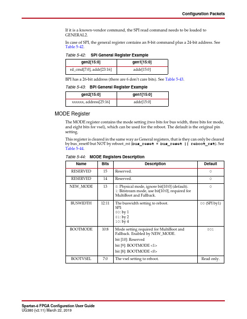
Configuration PacketsIf it is a known-vendor command, the SPI read command needs to be loaded to GENERAL2.In case of SPI, the general register contains an 8-bit command plus a 24-bit address. See Table 5-42.BPI has a 26-bit address (there are 6 don’t care bits). See Table 5-43.MODE RegisterThe MODE register contains the mode setting (two bits for bus width, three bits for mode, and eight bits for vsel), which can be used for the reboot. The default is the original pin setting.This register is cleared in the same way as General registers, that is they can only be cleared by bus_reset0 but NOT by reboot_rst (bus_reset = bus_reset || reboot_rst ). See Table 5-44.Table 5-42:SPI General Register Examplegen2[15:0]gen1[15:0]rd_cmd[7:0], addr[23:16]addr[15:0]Table 5-43:BPI General Register Examplegen2[15:0]gen1[15:0]xxxxxx, address[25:16]addr[15:0]Table 5-44:MODE Registers DescriptionName Bits DescriptionDefault RESERVED 15Reserved.0RESERVED 14Reserved.0NEW_MODE130: Physical mode, ignore bit[10:0] (default).1: Bitstream mode, use bit[10:0], required for MultiBoot and Fallback.0BUSWIDTH 12:11The buswidth setting to reboot.SPI:00: by 101: by 210: by 400 (SPI by1)BOOTMODE 10:8Mode setting required for MultiBoot and Fallback. Enabled by NEW_MODE.bit [10]: Reserved bit [9]: BOOTMODE <1>bit [8]: BOOTMODE <0>001BOOTVSEL 7:0The vsel setting to reboot.Read only.Chapter 5:Configuration DetailsiMPACT Access to Device IdentifierThe iMPACT software in ISE 10.1 (and later) tools can also read the device DNA value.readDna -p <position> is the batch command that reads the device DNA from theFPGA.Bitstream CompressionBy default, FPGA bitstreams are uncompressed. However, Spartan-6 FPGAs support basicbitstream compression. The compression is fairly simple, yet effective for someapplications. The ISE bitstream generator software examines the FPGA bitstream for anyduplicate configuration data frames. These duplicates occur often in these situations:•FPGA designs with unused block RAM or hardware multipliers.•FPGA designs with low logic utilization, such as when most of the FPGA array isempty.The ISE software can then generate a compressed FPGA bitstream. As the FPGAconfigures, the internal configuration controller copies the redundant data frame tomultiple locations. Compression is not supported for encrypted bitstreams.The amount of compression is non-deterministic. Changes to the source FPGA design cancause the size of the compressed bitstream to grow. Sparse, mostly empty FPGA designshave the greatest overall compression factor. Similarly, FPGA designs with an emptycolumn of block RAM have a high compression factor.The overall benefits of a compressed bitstream are:•Smaller memory footprint.•Faster programming time for nonvolatile memory.•Faster configuration time.Compression is enabled using the BitGen option -g compress.Parallel Platform Flash PROMs offer their own compression mechanisms. For more details,see the “XCFxxP Decompression and Clock Options” chapter in UG161, Platform FlashPROM User Guide.Chapter 2:Configuration Interface BasicsChapter 3:Boundary-Scan and JTAG ConfigurationChapter 5:Configuration DetailsConfiguration Watchdog Timer RegisterThe configuration watchdog timer (CWDT) register stores the value of the number of clock cycles that the FPGA will wait before the watchdog time-out (in which SYNCWORD is not received). The default is 64k clock cycles. The minimum value is 16h'0201.HC_OPT_REG RegisterThe HC_OPT_REG register can only be reset to default by por_b.GENERAL Registers 1, 2, 3, 4, and 5GENERAL1 and GENERAL2 registers are used to store loadable multiple configuration addresses for SPI and BPI.GENERAL3 and GENERAL4 registers have a similar function as GENERAL1 andGENERAL2, except that GENERAL3 and GENERAL4 store the golden bitstream address instead of the MultiBoot address.The GENERAL5 register is a 16-bit register that allows users to store and access any extra information desired for the fail-safe scheme. These register contents are untouched during a soft reboot.These registers are set by the bitstream. BitGen can be instructed not to write to these registers using the -g next_config_register_write:Disable command. This allows the ability to store user data in the FPGA between re-configuration attempts.If the second configuration needs a previously unknown SPI vendor command, the new vendor command has already been loaded in GENERAL2 from the bitstream by this point.Table 5-39:CWDT RegisterBits Value [15:0]16h'ffffTable 5-40:HC_OPT_REG DescriptionName Bits DescriptionDefault INIT_SKIP 60: Do not skip initialization.1: Skip initialization.0RESERVED5:0Reserved.011111Table 5-41:General RegistersName Bits DescriptionGENERAL1[15:0]The lower half of the multiple boot address.GENERAL2[15:0]15:8 – SPI opcode.7:0 – Higher half of the boot address.GENERAL3[15:0]The lower half of the golden bitstream address.GENERAL4[15:0]15:8 – SPI opcode.7:0 – Higher half of the golden boot address.GENERAL5[15:0]The user-defined scratchpad register.。
XC95108-10PQG100I中文资料

• Slew rate control on individual outputs • User programmable ground pin capability • Extended pattern security features for design
XC9500 concurrently • Available in 84-pin PLCC, 100-pin PQFP, 100-pin
TQFP, and 160-pin PQFP packages
Description
The XC95108 is a high-performance CPLD providing advanced in-system programming and test capabilities for general purpose logic integration. It is comprised of eight 36V18 Function Blocks, providing 2,400 usable gates with propagation delays of 7.5 ns. See Figure 2 for the architecture overview.
V
VIN
Input voltage relative to GND
–0.5 to VCC + 0.5
V
VTS TSTG
TJ
Voltage applied to 3-state output Storage temperature (ambient) Junction temperature
FPGA可编程逻辑器件芯片XC95288XL-10FG256I4124中文规格书
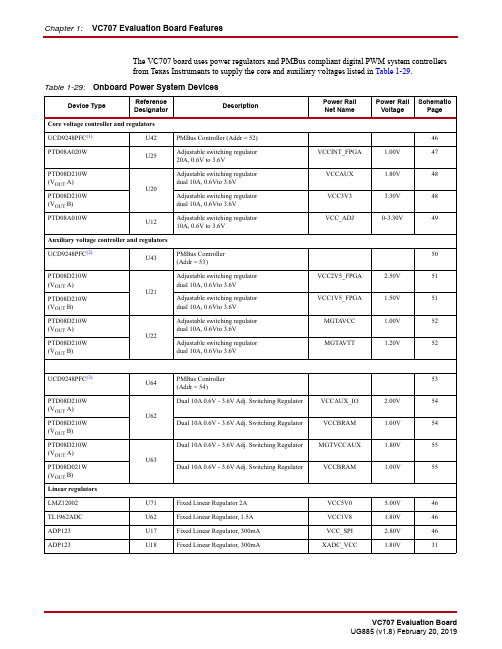
The VC707 board uses power regulators and PMBus compliant digital PWM system controllersfrom Texas Instruments to supply the core and auxiliary voltages listed in Table1-29.Table 1-29:Onboard Power System DevicesDevice Type ReferenceDesignatorDescriptionPower RailNet NamePower RailVoltageSchematicPageCore voltage controller and regulatorsUCD9248PFC(1)U42PMBus Controller (Addr=52)46PTD08A020WU25Adjustable switching regulator20A, 0.6V to 3.6VVCCINT_FPGA 1.00V47PTD08D210W(V OUT A)U20Adjustable switching regulatordual 10A, 0.6Vto 3.6VVCCAUX 1.80V48PTD08D210W (V OUT B)Adjustable switching regulatordual 10A, 0.6Vto 3.6VVCC3V3 3.30V48PTD08A010WU12Adjustable switching regulator10A, 0.6V to 3.6VVCC_ADJ0-3.30V49Auxiliary voltage controller and regulatorsUCD9248PFC(2)U43PMBus Controller(Addr=53)50PTD08D210W(V OUT A)U21Adjustable switching regulatordual 10A, 0.6Vto 3.6VVCC2V5_FPGA 2.50V51PTD08D210W (V OUT B)Adjustable switching regulatordual 10A, 0.6Vto 3.6VVCC1V5_FPGA 1.50V51PTD08D210W(V OUT A)U22Adjustable switching regulatordual 10A, 0.6Vto 3.6VMGTA VCC 1.00V52PTD08D210W (V OUT B)Adjustable switching regulatordual 10A, 0.6Vto 3.6VMGTA VTT 1.20V52UCD9248PFC(3)U64PMBus Controller(Addr=54)53PTD08D210W(V OUT A)U62Dual 10A 0.6V - 3.6V Adj. Switching Regulator VCCAUX_IO 2.00V54PTD08D210W(V OUT B)Dual 10A 0.6V - 3.6V Adj. Switching Regulator VCCBRAM 1.00V54PTD08D210W(V OUT A)U63Dual 10A 0.6V - 3.6V Adj. Switching Regulator MGTVCCAUX 1.80V55PTD08D021W(V OUT B)Dual 10A 0.6V - 3.6V Adj. Switching Regulator VCCBRAM 1.00V55 Linear regulatorsLMZ12002U71Fixed Linear Regulator 2A VCC5V0 5.00V46 TL1962ADC U62Fixed Linear Regulator, 1.5A VCC1V8 1.80V46 ADP123U17Fixed Linear Regulator, 300mA VCC_SPI 2.80V46 ADP123U18Fixed Linear Regulator, 300mA XADC_VCC 1.80V31Table 1-30 defines the voltage and current values for each power rail controlled by the UCD9248 PMBus controller at address 52 (U42).Table 1-31 defines the voltage and current values for each power rail controlled by the UCD9248 PMBus controller at address 53 (U43).Table 1-30:Power Rail Specifications for UCD9248 PMBus Controller at Address 52Shutdown Threshold (1)Rail Number Rail Name Schematic Rail NameN o m i n a l V O U T (V )P G O n T h r e s h o l d (V )P G O f f T h r e s h o l d (V )O n D e l a y (m s )R i s e T i m e (m s )O f f D e l a y (m s )F a l l T i m e (m s )V O U T O v e r F a u l t (V )I O U T O v e r F a u l t (A )T e m p O v e r F a u l t (°C )1Rail #1VCCINT_FPGA 10.90.8505101 1.1520902Rail #2VCCAUX 1.8 1.62 1.530551 2.0710.41903Rail #3VCC3V3 3.3 2.97 2.8050541 3.79510.41904Rail #4V ADJ1.81.621.535312.0710.4190Notes:1.The values defined in these columns are the voltage, current, and temperature thresholds that cause the regulator to shut down if the value is exceeded.Table 1-31:Power Rail Specifications for UCD9248 PMBus Controller at Address 53Shutdown Threshold (1)Rail Number Rail Name Schematic Rail NameN o m i n a l V O U T (V )P G O n T h r e s h o l d (V )P G O f f T h r e s h o l d (V )O n D e l a y (m s )R i s e T i m e (m s )O f f D e l a y (m s )F a l l T i m e (m s )V O U T O v e r F a u l t (V )I O U T O v e r F a u l t (A )T e m p O v e r F a u l t (°C )1Rail #1VCC2V5_FPGA 2.5 2.25 2.1250511 2.87510.41902Rail #2VCC1V5 1.5 1.35 1.2750501 1.72510.41903Rail #3MGTA VCC 10.90.850571 1.4510.41904Rail #4MGTA VTT1.21.081.025811.3810.4190Notes:1.The values defined in these columns are the voltage, current, and temperature thresholds that causes the regulator to shut down if the value is exceeded.Feature DescriptionsFor external measurements an XADC header (J19) is provided. This header can be used to provide analog inputs to the FPGA's dedicated VP/VN channel, and to the V AUXP[0]/V AUXN[0],V AUXP[8]/V AUXN[8] auxiliary analog input channels. Simultaneous sampling of Channel 0 and Channel 8 is supported.A user-provided analog signal multiplexer card can be used to sample additional external analog inputs using the 4 GPIO pins available on the XADC header as multiplexer address lines. Figure 1-35 shows the XADC header connections.Table 1-33 describes the XADC header J19 pin functions.Figure 1-35:XADC Header (J19)Table 1-33:XADC Header J19 PinoutNet Name J19 Pin Number DescriptionVN, VP 1, 2Dedicated analog input channel for the XADC.XADC_V AUX0P, N 3, 6Auxiliary analog input channel 0. Also supports use as I/O inputs when anti-alias capacitor is not present.XADC_V AUX8N, P7, 8Auxiliary analog input channel 8. Also supports use as I/O inputs when anti-alias capacitor is not present.DXP, DXN 9, 12Access to thermal diode.XADC_AGND 4, 5, 10Analog ground reference.XADC_VREF 11 1.25V reference from the board.XADC_VCC5V013Filtered 5V supply from board.XADC_VCC_HEADER14Analog 1.8V supply for XADC.V ADJ 15VCCO supply for bank which is the source of DIO pins.GND16Digital Ground (board) ReferenceXADC_GPIO_3, 2, 1, 019, 20, 17, 18Digital I/O. These pins should come from the same bank. These I/Os should not be shared with other functions because they are required to support 3-state operation.Chapter 1:VC707 Evaluation Board FeaturesAppendix B:VITA 57.1 FMC Connector Pinouts。
FPGA可编程逻辑器件芯片XC95144-10PQ160I中文规格书
Module 1:Introduction and Ordering Information DS099 (v3.1) June 27, 2013•Introduction•Features•Architectural Overview•Array Sizes and Resources•User I/O Chart•Ordering InformationModule 2: Functional DescriptionDS099 (v3.1) June 27, 2013•Input/Output Blocks (IOBs)•IOB Overview•SelectIO™ Interface I/O Standards •Configurable Logic Blocks (CLBs)•Block RAM•Dedicated Multipliers•Digital Clock Manager (DCM)•Clock Network•ConfigurationModule 3:DC and Switching CharacteristicsDS099 (v3.1) June 27, 2013•DC Electrical Characteristics•Absolute Maximum Ratings•Supply Voltage Specifications•Recommended Operating Conditions•DC Characteristics•Switching Characteristics•I/O Timing•Internal Logic Timing•DCM Timing•Configuration and JT AG Timing Module 4: Pinout DescriptionsDS099 (v3.1) June 27, 2013•Pin Descriptions•Pin Behavior During Configuration•Package Overview•Pinout T ables•FootprintsSpartan-3 FPGA FamilyData SheetDS099 June 27, 2013Product SpecificationTable 35:Recommended Operating Conditions for User I/Os Using Single-Ended StandardsSignal Standard (IOSTANDARD)V CCO V REF V IL V IH Min (V)Nom (V)Max (V)Min (V)Nom (V)Max (V)Max (V)Min (V)GTL(3)–––0.740.80.86V REF – 0.05V REF + 0.05 GTL_DCI– 1.2–0.740.80.86V REF – 0.05V REF + 0.05 GTLP(3)–––0.881 1.12V REF – 0.1V REF + 0.1 GTLP_DCI– 1.5–0.881 1.12V REF – 0.1V REF + 0.1 HSLVDCI_15 1.4 1.5 1.6–0.75–V REF – 0.1V REF + 0.1 HSLVDCI_18 1.7 1.8 1.9–0.9–V REF – 0.1V REF + 0.1 HSLVDCI_25 2.3 2.5 2.7– 1.25–V REF – 0.1V REF + 0.1 HSLVDCI_33 3.0 3.3 3.465– 1.65–V REF – 0.1V REF + 0.1 HSTL_I, HSTL_I_DCI 1.4 1.5 1.60.680.750.9V REF – 0.1V REF + 0.1 HSTL_III,HSTL_III_DCI 1.4 1.5 1.6–0.9–V REF – 0.1V REF + 0.1HSTL_I_18,HSTL_I_DCI_18 1.7 1.8 1.90.80.9 1.1V REF – 0.1V REF + 0.1 HSTL_II_18,HSTL_II_DCI_18 1.7 1.8 1.9–0.9–V REF – 0.1V REF + 0.1HSTL_III_18,HSTL_III_DCI_18 1.7 1.8 1.9– 1.1–V REF – 0.1V REF + 0.1 LVCMOS12 1.14 1.2 1.3–––0.37V CCO0.58V CCO LVCMOS15,LVDCI_15,LVDCI_DV2_151.4 1.5 1.6–––0.30V CCO0.70V CCOLVCMOS18,LVDCI_18,LVDCI_DV2_181.7 1.8 1.9–––0.30V CCO0.70V CCOLVCMOS25(4,5),LVDCI_25,LVDCI_DV2_25(4)2.3 2.5 2.7–––0.7 1.7LVCMOS33,LVDCI_33,LVDCI_DV2_33(4)3.0 3.3 3.465–––0.8 2.0 LVTTL 3.0 3.3 3.465–––0.8 2.0PCI33_3(7) 3.0 3.3 3.465–––0.30V CCO0.50V CCO SSTL18_I,SSTL18_I_DCI 1.7 1.8 1.90.8330.9000.969V REF – 0.125V REF + 0.125 SSTL18_II 1.7 1.8 1.90.8330.9000.969V REF – 0.125V REF + 0.125 SSTL2_I,SSTL2_I_DCI 2.3 2.5 2.7 1.15 1.25 1.35V REF – 0.15V REF + 0.15 SSTL2_II,SSTL2_II_DCI 2.3 2.5 2.7 1.15 1.25 1.35V REF – 0.15V REF + 0.15 Notes:1.Descriptions of the symbols used in this table are as follows:V CCO – the supply voltage for output drivers as well as LVCMOS, LVTTL, and PCI inputsV REF – the reference voltage for setting the input switching thresholdV IL – the input voltage that indicates a Low logic levelV IH – the input voltage that indicates a High logic level2.For device operation, the maximum signal voltage (V IH max) may be as high as V IN max. See Table28.3.Because the GTL and GTLP standards employ open-drain output buffers, V CCO lines do not supply current to the I/O circuit, rather this current isprovided using an external pull-up resistor connected from the I/O pin to a termination voltage (V TT). Nevertheless, the voltage applied to the associated V CCO lines must always be at or above V TT and I/O pad voltages.4.There is approximately 100mV of hysteresis on inputs using LVCMOS25 or LVCMOS33 standards.5.All dedicated pins (M0-M2, CCLK, PROG_B, DONE, HSWAP_EN, TCK, TDI, TDO, and TMS) use the LVCMOS standard and draw power from theV CCAUX rail (2.5V). The dual-purpose configuration pins (DIN/D0, D1-D7, CS_B, RDWR_B, BUSY/DOUT, and INIT_B) use the LVCMOS standard before the user mode. For these pins, apply 2.5V to the V CCO Bank 4 and V CCO Bank 5 rails at power-on and throughout configuration. For information concerning the use of 3.3V signals, see 3.3V-T olerant Configuration Interface, page47.6.The Global Clock Inputs (GCLK0-GCLK7) are dual-purpose pins to which any signal standard can be assigned.7.For more information, see XAPP457.Table 36:DC Characteristics of User I/Os Using Single-Ended StandardsSignal Standard (IOSTANDARD) and Current Drive Attribute (mA)Test Conditions Logic Level Characteristics I OL(mA)I OH(mA)V OLMax (V)V OHMin (V)GTL32–0.4–GTL_DCI Note 3Note 3GTLP36–0.6–GTLP_DCI Note 3Note 3HSLVDCI_15Note 3Note 30.4V CCO – 0.4 HSLVDCI_18HSLVDCI_25HSLVDCI_33HSTL_I8–80.4V CCO – 0.4 HSTL_I_DCI Note 3Note 3HSTL_III24–80.4V CCO – 0.4 HSTL_III_DCI Note 3Note 3HSTL_I_188–80.4V CCO – 0.4 HSTL_I_DCI_18Note 3Note 3HSTL_II_1816–160.4V CCO – 0.4 HSTL_II_DCI_18Note 3Note 3HSTL_III_1824–80.4V CCO – 0.4 HSTL_III_DCI_18Note 3Note 3LVCMOS12(4)22–20.4V CCO – 0.4 44–466–6LVCMOS15(4)22–20.4V CCO – 0.4 44–466–688–81212–12LVDCI_15,LVDCI_DV2_15Note 3Note 3LVCMOS18(4)22–20.4V CCO – 0.4 44–466–688–81212–121616–16LVDCI_18,LVDCI_DV2_18Note 3Note 3LVCMOS25(4,5)22–20.4V CCO – 0.4 44–466–688–81212–121616–162424–24LVDCI_25,LVDCI_DV2_25Note 3Note 3。
FPGA可编程逻辑器件芯片XC9572-15PQ100I中文规格书
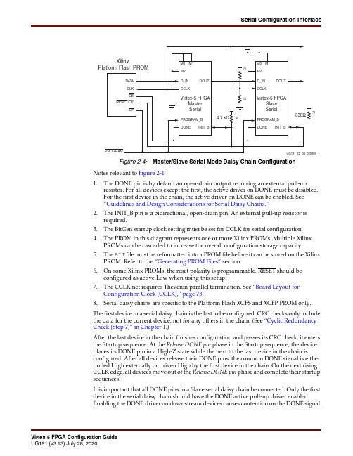
Serial Configuration InterfaceNotes relevant to Figure 2-4:1.The DONE pin is by default an open-drain output requiring an external pull-upresistor. For all devices except the first, the active driver on DONE must be disabled.For the first device in the chain, the active driver on DONE can be enabled. See “Guidelines and Design Considerations for Serial Daisy Chains.”2.The INIT_B pin is a bidirectional, open-drain pin. An external pull-up resistor is required.3.The BitGen startup clock setting must be set for CCLK for serial configuration.4.The PROM in this diagram represents one or more Xilinx PROMs. Multiple Xilinx PROMs can be cascaded to increase the overall configuration storage capacity.5.The BIT file must be reformatted into a PROM file before it can be stored on the Xilinx PROM. Refer to the “Generating PROM Files” section.6.On some Xilinx PROMs, the reset polarity is programmable. RESET should be configured as active Low when using this setup.7.The CCLK net requires Thevenin parallel termination. See “Board Layout for Configuration Clock (CCLK),” page 73.8.Serial daisy chains are specific to the Platform Flash XCFS and XCFP PROM only.The first device in a serial daisy chain is the last to be configured. CRC checks only include the data for the current device, not for any others in the chain. (See “Cyclic Redundancy Check (Step 7)” in Chapter 1.)After the last device in the chain finishes configuration and passes its CRC check, it enters the Startup sequence. At the Release DONE pin phase in the Startup sequence, the device places its DONE pin in a High-Z state while the next to the last device in the chain isconfigured. After all devices release their DONE pins, the common DONE signal is either pulled High externally or driven High by the first device in the chain. On the next rising CCLK edge, all devices move out of the Release DONE pin phase and complete their startup sequences.It is important that all DONE pins in a Slave serial daisy chain be connected. Only the first device in the serial daisy chain should have the DONE active pull-up driver enabled. Enabling the DONE driver on downstream devices causes contention on the DONE signal.Figure 2-4:Master/Slave Serial Mode Daisy Chain Configuration09PlChapter 2:Configuration InterfacesMixed Serial Daisy ChainsVirtex-5 devices can be daisy-chained with the Virtex, Spartan™-II, Virtex-E, Spartan-IIE,Virtex-II, Virtex-II Pro, Spartan-3, and Virtex-4 families. There are three important designconsiderations when designing a mixed serial daisy chain:∙Many older FPGA devices cannot accept as fast a CCLK frequency as a Virtex-5 devicecan generate. Select a configuration CCLK speed supported by all devices in thechain.∙Virtex-5 devices should always be at the beginning of the serial daisy chain, witholder family devices located at the end of the chain.∙All Virtex device families have similar BitGen options. The guidelines provided forVirtex-5 BitGen options should be applied to all Virtex devices in a serial daisy chain.∙The number of configuration bits that a device can pass through its DOUT pin islimited. This limit varies for different families (Table2-3). The sum of the bitstreamlengths for all downstream devices must not exceed the number in Table2-3 for eachfamily.Table 2-3:Maximum Number of Configuration Bits, Various Device FamiliesArchitecture Maximum DOUT BitsVirtex-5, Virtex-4, Virtex-II Pro, and Virtex-II Devices32 x (227 – 1) = 4,294,967,264Spartan-3 Devices32 x (227 – 1) = 4,294,967,264Virtex, Virtex-E, Spartan-II, and Spartan-IIE Devices32 x (220 – 1) = 33,554,216 Guidelines and Design Considerations for Serial Daisy ChainsThere are a number of important considerations for serial daisy chains:Startup Sequencing (GTS)GTS should be released before DONE or during the same cycle as DONE to ensure theVirtex-5 device is operational when all DONE pins have been released.Active DONE DriverAll devices except the first should disable the driver on the DONE pin (refer to the BitGensection of the Development System Reference Guide for software settings). The first device ina chain is programmed last:∙DriveDone is disabled (all devices except the first)∙DriveDone is enabled (first device)Alternatively, the driver can be disabled for all DONE pins and an external pull-up resistorcan be added to pull the signal High after all devices have released it.Connect All DONE PinsIt is important to connect the DONE pins for all devices in a serial daisy chain. Failing toconnect the DONE pins can cause configuration to fail. For debugging purposes, it is oftenhelpful to have a way of disconnecting individual DONE pins from the common DONEsignal, so that devices can be individually configured through the serial or JTAG interface.Serial Configuration InterfaceDONE Pin Rise TimeAfter all DONE pins are released, the DONE pin should rise from logic 0 to logic 1 in oneCCLK cycle. External pull-up resistors are required. If additional time is required for theDONE signal to rise, the BitGen donepipe option can be set for all devices in the serialdaisy chain. (Refer to the BitGen section of the Development System Reference Guide forsoftware settings.)Ganged Serial ConfigurationMore than one device can be configured simultaneously from the same bitstream using aganged serial configuration setup (Figure2-5). In this arrangement, the serial configurationpins are tied together such that each device sees the same signal transitions. One device istypically set for Master serial mode (to drive CCLK) while the others are set for Slave serialmode. For ganged serial configuration, all devices must be identical. Configuration can bedriven from a configuration PROM or from an external configuration controller.u g191_c2_31_090808Figure 2-5:Ganged Serial ConfigurationNotes relevant to Figure2-5:1.For ganged serial configuration, the optional DONE driver must be disabled for alldevices if one device is set for Master mode because each device might not start up onexactly the same CCLK cycle. An external pull-up resistor is required in this case.2.The INIT_B pin is a bidirectional, open-drain pin. An external pull-up resistor isrequired.3.The BitGen startup clock setting must be set for CCLK for serial configuration.Board Layout for Configuration Clock (CCLK)Chapter 2:Configuration Interfaces。
FPGA可编程逻辑器件芯片XC95144XL-10TQG144I中文规格书
Feature DescriptionsVITA 57.1 FMC1 HPC Connector (Partially Populated)[Figure1-2, callout 30]The VC707 board implements two instances of the FMC HPC VITA 57.1 specification connector.This section discusses the FMC1 HPC J35 connector.Note:The FMC1 HPC J35 connector is a keyed connector oriented so that a plug-on card facesaway from the VC707 board.The VITA 57.1 FMC standard calls for two connector densities: a high pin count (HPC) and a lowpin count (LPC) implementation. A 400 pin 10x40 position connector form factor is used for bothversions. The HPC version is fully populated with all 400 pins present. The LPC version is partiallypopulated with 160 pins.The 10x40 rows of an FMC HPC connector provides pins for up to:•160 single-ended or 80 differential user-defined signals•10 GTX transceivers• 2 GTX clocks• 4 differential clocks•159 ground and 15 power connectionsThe VC707 board FMC1 HPC connector J35 implements a subset of the maximum signal and clockconnectivity capabilities:•80 differential user-defined pairs•34 LA pairs (LA00-LA33)•24 HA pairs (HA00-HA23)•22 HB pairs (HB00-HB21)•8 GTX transceivers• 2 GTX clocks• 2 differential clocksThe FMC1 HPC signals are distributed across GTX Quads 118 and 119. Each Quad has the VCCOvoltage connected to V ADJ.Note:The VC707 board VADJ voltage for the FMC1 HPC (J35) connector is determined by theFMC VADJ power sequencing logic described in FMC_VADJ Voltage Control.VITA 57.1 FMC2 HPC Connector (Partially Populated)[Figure1-2, callout 31]The VC707 board implements two instances of the FMC HPC VITA 57.1 specification connector.This section discusses the FMC2 HPC J37 connector.Note:The FMC2 HPC J37 connector is a keyed connector oriented so that a plug-on card facesaway from the VC707 board.The FMC standard calls for two connector densities: a High Pin Count (HPC) and a Low Pin Count(LPC) implementation. A 400pin 10x40 position connector form factor is used for both versions.The HPC version is fully populated with all 400 pins present. The LPC version is partially populatedwith 160 pins.Chapter 1:VC707 Evaluation Board FeaturesXADC Analog-to-Digital Converter7series FPGAs provide an analog front end XADC block. The XADC block includes a dual 12-bit,1MSPS analog-to-digital convertor (ADC) and on-chip sensors. See 7Series FPGAs XADC Dual12-Bit 1MSPS Analog-to-Digital Converter User Guide (UG480) [Ref11] for details on thecapabilities of the analog front end. Figure1-34 shows the XADC block diagram.Figure 1-34:XADC Block DiagramThe VC707 board supports both the internal FPGA sensor measurements and the externalmeasurement capabilities of the XADC. Internal measurements of the die temperature, VCCINT,VCCAUX, and VCCBRAM are available. The VC707 board VCCINT and VCCBRAM areprovided by a common 1.0 V supply.Jumper J42 can be used to select either an external differential voltage reference (VREF) or on-chipvoltage reference for the analog-to-digital converter.Feature DescriptionsFor external measurements an XADC header (J19) is provided. This header can be used to provide analog inputs to the FPGA's dedicated VP/VN channel, and to the V AUXP[0]/V AUXN[0],V AUXP[8]/V AUXN[8] auxiliary analog input channels. Simultaneous sampling of Channel 0 and Channel 8 is supported.A user-provided analog signal multiplexer card can be used to sample additional external analog inputs using the 4 GPIO pins available on the XADC header as multiplexer address lines. Figure 1-35 shows the XADC header connections.Table 1-33 describes the XADC header J19 pin functions.Figure 1-35:XADC Header (J19)Table 1-33:XADC Header J19 PinoutNet Name J19 Pin Number DescriptionVN, VP 1, 2Dedicated analog input channel for the XADC.XADC_V AUX0P, N 3, 6Auxiliary analog input channel 0. Also supports use as I/O inputs when anti-alias capacitor is not present.XADC_V AUX8N, P7, 8Auxiliary analog input channel 8. Also supports use as I/O inputs when anti-alias capacitor is not present.DXP, DXN 9, 12Access to thermal diode.XADC_AGND 4, 5, 10Analog ground reference.XADC_VREF 11 1.25V reference from the board.XADC_VCC5V013Filtered 5V supply from board.XADC_VCC_HEADER14Analog 1.8V supply for XADC.V ADJ 15VCCO supply for bank which is the source of DIO pins.GND16Digital Ground (board) ReferenceXADC_GPIO_3, 2, 1, 019, 20, 17, 18Digital I/O. These pins should come from the same bank. These I/Os should not be shared with other functions because they are required to support 3-state operation.Appendix A:Default Switch and Jumper SettingsAppendix B:VITA 57.1 FMC Connector Pinouts。
FPGA可编程逻辑器件芯片XC95144XL-7TQG100I中文规格书

Chapter 5:Configuration DetailsConfiguration Options Register (COR1 and COR2)The Configuration Options Register is used to set certain configuration options for thedevice. The name of each bit position in COR1 and COR2 is given in Table5-36.Table 5-36:Configuration Options (COR1 and COR2) DescriptionsRegister Field Bit Index Description BitGen DefaultCOR1DRIVE_AWAKE150: Does not drive the awake pin (open drain).1: Actively drives the awake pin.RESERVED14:5Reserved.0110111000CRC_BYPASS4Does not check against the updated CRC value.0DONE_PIPE30: No pipeline stage for DONEIN.1: Add pipeline stage to DONEIN.DRIVE_DONE20: DONE pin is open drain.1: DONE pin is actively driven High.SSCLKSRC1:0Startup sequence clock.00: CCLK.01: UserClk.1x: TCK.00COR2RESET_ON_ERROR15Option to fallback when a crc_error occurs.0: Disable reset on error.1: Enable reset on error.0 RESERVED14:12Reserved000DONE_CYCLE11:9Startup phase in which DONE pin is released.(001,010,011,100,101,110)100LCK_CYCLE8:6Stall in this startup phase until DCM or PLL lock isasserted. (001,010,011,100,101,110,111<Nowait>)111 (No wait)GTS_CYCLE5:3Startup phase in which I/Os switch from 3-state to userdesign.(000<Keep>, 001,010,011,100,101,110,111<Done>)101GWE_CYCLE2:0Startup phase in which the global write enable is asserted.(000<Keep>, 001,010,011,100,101,110,111<Done>)110Spartan-6 FPGA Unique Device Identifier (Device DNA)Spartan-6 FPGA Unique Device Identifier (Device DNA)Spartan-6 FPGAs contain an embedded, unique device identifier (device DNA). Theidentifier is nonvolatile, permanently programmed into the FPGA, and is unchangeable,making it tamper resistant.The FPGA application accesses the identifier value using the Device DNA Access Port(DNA_PORT) design primitive, shown in Figure5-13.Figure 5-13:Spartan-6 FPGA DNA_PORT Design PrimitiveIdentifier ValueAs shown in Figure5-14, the device DNA value is 57 bits long. The two most-significantbits are always 1 and 0. The remaining 55 bits are unique to a specific Spartan-6 FPGA.OperationFigure5-14 shows the general functionality of the DNA_PORT design primitive. An FPGAapplication must first instantiate the DNA_PORT primitive, shown in Figure5-13, within adesign.Figure 5-14:DNA_PORT OperationTo read the device DNA, the FPGA application must first transfer the identifier value intothe DNA_PORT output shift register. The READ input must be asserted during a risingedge of CLK, as shown in Table5-51. This action parallel loads the output shift registerwith all 57 bits of the identifier. Because bit 56 of the identifier is always 1, the DOUToutput is also 1. The READ operation overrides a SHIFT operation.To continue reading the identifier values, SHIFT must be asserted, followed by a risingedge of CLK, as shown in Table5-51. This action causes the output shift register to shift itscontents toward the DOUT output. The value on the DIN input is shifted into the shiftregister.Chapter 5:Configuration DetailsA Low-to-High transition on SHIFT should be avoided when CLK is High because this causes a spurious initial clock edge. Ideally, SHIFT should only be asserted when CLK is Low or on a falling edge of CLK.If both READ and SHIFT are Low, the output shift register holds its value and DOUT remains unchanged.Identifier Memory SpecificationsThe unique FPGA identifier value is retained for a minimum of ten years of continuous usage under worst-case recommended operating conditions. The identifier can be read, using the READ operation defined in Table 5-51, a minimum of 30 million cycles, which roughly correlates to one read operation every 11 seconds for the operating lifetime of the Spartan-6FPGA.Extending Identifier LengthAs shown in Figure 5-15, most applications that use the DNA_PORT primitive tie the DIN data input to a static value.Table 5-51:DNA_PORT Operations Operation DIN READ SHIFT CLK Shift Register DOUTHOLD X 00X Hold previous value Hold previous value READ X 1X ↑Parallel load with 57-bit IDBit 56 of identifier, which is always 1SHIFTDIN1↑Shift DIN into bit 0, shift contents of ShiftRegister toward DOUTBit 56 of Shift RegisterNotes:X = Don’t care↑= Rising clock edgeFigure 5-15:Shift in ConstantChapter 6:Readback and Configuration VerificationChapter 7:Reconfiguration and MultiBoot。
- 1、下载文档前请自行甄别文档内容的完整性,平台不提供额外的编辑、内容补充、找答案等附加服务。
- 2、"仅部分预览"的文档,不可在线预览部分如存在完整性等问题,可反馈申请退款(可完整预览的文档不适用该条件!)。
- 3、如文档侵犯您的权益,请联系客服反馈,我们会尽快为您处理(人工客服工作时间:9:00-18:30)。
Chapter 1:Configuration OverviewCreating an Encrypted BitstreamBitGen, provided with the Xilinx ISE software, can generate encrypted as well as non-encrypted bitstreams. For AES bitstream encryption, the user specifies a 256-bit key as aninput to BitGen. BitGen in turn generates an encrypted bitstream file (BIT) and anencryption key file (NKY).For specific BitGen commands and syntax, refer to the Development System Reference Guide.Loading the Encryption KeyThe encryption key can only be loaded onto a Virtex-5 device through the JTAG interface.The iMPACT tool, provided with the Xilinx ISE software, can accept the NKY file as aninput and program the device with the key through JTAG, using a supported Xilinxprogramming cable.To program the key, the device enters a special key-access mode using theISC_PROGRAM_KEY instruction. In this mode, all FPGA memory, including theencryption key and configuration memory, is cleared. After the key is programmed andthe key-access mode is exited, the key cannot be read out of the device by any means, andit cannot be reprogrammed without clearing the entire device. The key-access mode istransparent to most users.Loading Encrypted BitstreamsOnce the device has been programmed with the correct encryption key, the device can beconfigured with an encrypted bitstream. After configuration with an encrypted bitstream,it is not possible to read the configuration memory through JTAG or SelectMAP readback,regardless of the BitGen security setting.While the device holds an encryption key, a non-encrypted bitstream can be used toconfigure the device; in this case the key is ignored. After configuring with a non-encrypted bitstream, readback is possible (if allowed by the BitGen security setting). Theencryption key still cannot be read out of the device, preventing the use of Trojan Horsebitstreams to defeat the Virtex-5 encryption scheme.The method of configuration is not affected by encryption. The configuration bitstream canbe delivered in any mode (Serial, JTAG, or any x8 parallel modes) from any configurationsolution (PROM, System ACE™ controller, etc.). The x16 and x32 bus widths are notsupported for encrypted bitstreams. Configuration timing and signaling are alsounaffected by encryption.The encrypted bitstream must configure the entire device because partial reconfigurationthrough any configuration interface is not permitted for encrypted bitstreams. Afterconfiguration, the device cannot be reconfigured without toggling the PROGRAM_B pin,cycling power, or issuing the JPROGRAM instruction. Fallback reconfiguration andIPROG reconfiguration (see “Fallback MultiBoot,” page153) are disabled after encryptionis turned on. Readback is available through the ICAP primitive (see “Bitstream Encryptionand Internal Configuration Access Port (ICAP)”). None of these events resets the key ifV BATT or V CCAUX is maintained.A mismatch between the key in the encrypted bitstream and the key stored in the devicecauses configuration to fail with the INIT_B pin going Low and the DONE pin remainingLow.Bitstream EncryptionBitstream Encryption and Internal Configuration Access Port (ICAP) The Internal Configuration Access Port (ICAP) primitive provides the user logic withaccess to the Virtex-5 configuration interface. The ICAP interface is similar to theSelectMAP interface, although the restrictions on readback for the SelectMAP interface donot apply to the ICAP interface after configuration. Users can perform readback throughthe ICAP interface even if bitstream encryption is used. Unless the designer wires the ICAPinterface to user I/O, this interface does not offer attackers a method for defeating theVirtex-5 AES encryption scheme.Users concerned about the security of their design should not:∙Wire the ICAP interface to user I/O-or-∙Instantiate the ICAP primitive.Like the other configuration interfaces, the ICAP interface does not provide access to thekey register.V BATTThe encryption key memory cells are volatile and must receive continuous power to retaintheir contents. During normal operation, these memory cells are powered by the auxiliaryvoltage input (V CCAUX), although a separate V BATT power input is provided for retainingthe key when V CCAUX is removed. Because V BATT draws very little current (on the order ofnanoamperes), a small watch battery is suitable for this supply. (To estimate the battery life,refer to V BATT DC Characteristics in DS202, Virtex-5 Data Sheet: DC and SwitchingCharacteristics and the battery specifications.) At less than a 100nA load, the endurance ofthe battery should be limited only by its shelf life.V BATT does not draw any current and can be removed while V CCAUX is applied. V BATTcannot be used for any purpose other than retaining the encryption keys when V CCAUX isremoved.Chapter 1:Configuration OverviewSelectMAP Configuration Interface PROM files for ganged serial configuration are identical to the PROM files used toconfigure single devices. There are no special PROM file considerations.SelectMAP Configuration InterfaceThe SelectMAP configuration interface (Figure2-6) provides an 8-bit, 16-bit, or 32-bitbidirectional data bus interface to the Virtex-5 configuration logic that can be used for bothconfiguration and readback. (For details, refer to Chapter7, “Readback and ConfigurationVerification.”) The bus width of SelectMAP is automatically detected (see “Bus Width AutoDetection”).CCLK is an output in Master SelectMAP mode; in Slave SelectMAP, CCLK is an input. Oneor more Virtex-5 devices can be configured through the SelectMAP bus.There are four methods of configuring an FPGA in SelectMAP mode:∙Single device Master SelectMAP∙Single device Slave SelectMAP∙Multiple device SelectMAP bus∙Multiple device ganged SelectMAPTable2-4 describes the SelectMAP configuration interface.Figure 2-6:Virtex-5 Device SelectMAP Configuration InterfaceTable 2-4:Virtex-5 Device SelectMAP Configuration Interface PinsPin Name Type Dedicatedor Dual-PurposeDescriptionM[2:0]Input Dedicated Mode pins - determine configuration modeCCLK Input andOutputDedicatedConfiguration clock source for all configurationmodes except JTAGD[31:0]Three-StateBidirectionalDual-PurposeConfiguration and readback data bus, clockedon the rising edge of CCLK. See “Parallel BusBit Order” and Table1-2.BU S YDONECCLKPROGRAM_BINIT_BD[31:0]M[2:0]C S_BRDWR_BC S O_BUG191_c2_10_072407Board Layout for Configuration Clock (CCLK)。