MD1810六级能效(5V-1A)-DEMO-TEST-REPORT 24
施耐德最新变频器-ATV御程系列变频器

ATV御程系列 不仅仅只是一款变频器
>> 标准单机与工程型柜机最大至 1500kW >> 轻重载完美结合(轻载 110%,重载 150%),选型更为灵活 >> 集成双直流电抗器,更有效抑制谐波影响 >> 业界唯一标配 3C3、3S3 恶劣环境认证 >> -15oC…50oC 工作温度(无需降容运行),最高可达 60oC(需降容) >> 最高运行海拔为 4800 米 >> 标配中文高级图形显示终端(IP 65 防护等级,mini-USB 端口数据传输,数据
3.2
HD 1.5 2
3.1
2.9
2.4
ND 3
-
5.8
5.1
4.2
HD 2.2 3
4.5
4.0
3.3
ND 4
5
7.6
6.7
5.6
HD 3
-
6
5.4
4.5
ND 5.5 7 1/2 10.4
9.1
7.6
HD 4
5
8
7.2
6.0
ND 7.5 10
13.8
11.9
9.9
HD 5.5 7 1/2 10.5
9.2
(1) 标示电机功率和最大预期短路电流Isc的典型值 (2) ND(Normal Duty):轻载 110%负载,HD(Heavy Duty):重载 150%负载 (3) 型号ATV650U07N4...D90N4将于2014年9月份上市。
5
选型指南IP21
目标市场
• 供水及污水处理 • 石油天然气 • 采矿、冶金及建材 • 食品饮料
计,采用紧凑的模块化结构,非常适合初 (施耐德电气绿色生态标志),确保您的
MAX1818EUT18-TG16中文资料

For pricing, delivery, and ordering information, please contact Maxim Direct at 1-888-629-4642,or visit Maxim's website at .General DescriptionThe MAX1818 low-dropout linear regulator operates from a +2.5V to +5.5V supply and delivers a guaran-teed 500mA load current with low 120mV dropout. The high-accuracy (±1%) output voltage is preset at an internally trimmed voltage (see Selector Guide ) or can be adjusted from 1.25V to 5.0V with an external resis-tive divider.An internal PMOS pass transistor allows the low 125µA supply current to remain independent of load, making this device ideal for portable battery-operated equip-ment such as personal digital assistants (PDAs), cellu-lar phones, cordless phones, base stations, and notebook computers.Other features include an active-low open-drain reset output that indicates when the output is out of regula-tion, a 0.1µA shutdown, short-circuit protection, and thermal shutdown protection. The device is available in a miniature 800mW 6-pin SOT23 package.ApplicationsNotebook ComputersCellular and Cordless Telephones Personal Digital Assistants (PDAs)Palmtop Computers Base Stations USB Hubs Docking StationsFeatures♦Guaranteed 500mA Output Current ♦Low 120mV Dropout at 500mA♦±1% Output Voltage AccuracyPreset at 1.5V, 1.8V, 2.0V, 2.5V, 3.3V, 5V Adjustable from 1.25V to 5.0V ♦Power OK Output♦Low 125µA Ground Current ♦0.1µA Shutdown Current ♦Thermal Overload Protection ♦Output Current Limit♦Tiny 800mW 6-Pin SOT23 PackageMAX1818500mA Low-DropoutLinear Regulator in SOT23________________________________________________________________Maxim Integrated Products 119-1860; Rev 2; 6/08Ordering Information*Insert the desired two-digit suffix (see Selector Guide) into the blanks to complete the part number.Typical Operating CircuitPin ConfigurationNote :The MAX1818 requires a special solder temperature profile described in the Absolute Maximum Ratings section.T = Tape and reel.#Denotes an RoHS-compliant package.Selector Guide appears at end of data sheet.M A X 1818500mA Low-DropoutLinear Regulator in SOT23ABSOLUTE MAXIMUM RATINGSELECTRICAL CHARACTERISTICSStresses beyond those listed under “Absolute Maximum Ratings” may cause permanent damage to the device. These are stress ratings only, and functional operation of the device at these or any other conditions beyond those indicated in the operational sections of the specifications is not implied. Exposure to absolute maximum rating conditions for extended periods may affect device reliability.IN,SHDN ,POK, SET to GND...................................-0.3V to +6V OUT to GND ................................................-0.3V to (V IN + 0.3V)Output Short-Circuit Duration...............................................1min Continuous Power Dissipation (T A = +70°C) (Note 1)6-Pin SOT23 (derate 10mW/°C above +70°C)..............800mWOperating Temperature Range ...........................-40°C to +85°C Junction Temperature......................................................+150°C Storage Temperature Range.............................-65°C to +150°C Lead Temperature (soldering, 10s) (Note 2)...................+300°CNote 1:Thermal properties are specified with product mounted on PC board with one square-inch of copper area and still air. Withminimal copper, the SOT23 package dissipates 712mW at +70°C. With a quarter square inch of copper, it will dissipate 790mW at +70°C. Copper should be equally shared between the IN, OUT, and GND pins.Note 2:This device is constructed using a unique set of packaging techniques that imposes a limit on the thermal profile to whichthe device can be exposed during board-level solder attach and rework. The limit permits only the use of the solder profiles recommended in the industry standard specification, IPC JEDEC-J-STD-020A, paragraph 7.6, Table 3 for the IR/VPR and convection reflow. Preheating is required. Hand or wave soldering is not allowed.MAX1818500mA Low-DropoutLinear Regulator in SOT23_______________________________________________________________________________________3ELECTRICAL CHARACTERISTICS (continued)Note 4:The Dropout Voltage is defined as V IN - V OUT , when V OUT is 100mV below the value of V OUT measured for V IN = V OUT(NOM)+ 500mV. Since the minimum input voltage is 2.5V, this specification is only meaningful when V OUT(NOM)> 2.5V. For V OUT(NOM)between 2.5V and 3.5V, use the following equations: Typical Dropout = -93mV/V ✕V OUT(NOM)+ 445mV;Guaranteed Maximum Dropout = -137mV/V ✕V OUT(NOM)+7004mV. For V OUT(NOM)> 3.5V, Typical Dropout = 120mV;Maximum Dropout = 220mV.Typical Operating Characteristics(V IN = (V OUT + 500mV) or +2.5V, whichever is greater; SHDN = IN, C IN = 1µF, C OUT = 3.3µF, T A = +25°C, unless otherwise noted.)5025125100751501752252002500 1.0 1.50.5 2.0 2.5 3.0 3.5 4.0 4.5 5.0 5.5GROUND PIN CURRENT vs. INPUT VOLTAGEINPUT VOLTAGE (V)G R O U N D P I N C U R R E N T (μA )4070558513014511510016000.20.30.40.50.10.60.70.80.9 1.0LOAD CURRENT (A)G R O U N D P I N C U R R E N T (μA )GROUND PIN CURRENT vs. LOAD CURRENT110130120150140160170-4010-15356085TEMPERATURE (°C)G R O U N D P I N C U R R E N T (μA )GROUND PIN CURRENT vs. TEMPERATUREM A X 1818500mA Low-DropoutLinear Regulator in SOT234_______________________________________________________________________________________Typical Operating Characteristics (continued)(V IN = (V OUT + 500mV) or +2.5V, whichever is greater; SHDN = IN, C IN = 1µF, C OUT = 3.3µF, T A = +25°C, unless otherwise noted.)060301209015018000.20.10.30.40.5LOAD CURRENT (A)D R O P O U T V O L T A GE (m V )DROPOUT VOLTAGE vs. LOAD CURRENT-3.0-2.0-2.5-1.5-1.0-0.500.51.01.52.02.53.0LOAD CURRENT (A)O U T P U T V O L T A G E A C C U R A C Y (%)0.20.30.40.10.50.60.70.90.8 1.0OUTPUT VOLTAGE ACCURACYvs. LOAD CURRENT-3.0-2.0-2.5-1.5-1.0-0.500.51.01.52.02.53.0-40-1510356085TEMPERATURE (°C)O U T P U T V O L T A G E A C C U R A C Y (%)OUTPUT VOLTAGE ACCURACYvs. TEMPERATUREPOWER-SUPPLY REJECTION RATIOvs. FREQUENCY8002010P S R R (d B )40305060700.010.11101001000FREQUENCY (kHz)LINE TRANSIENTMAX1818 toc08V INV OUT2.5V 10m V /d i v3.5V 100μs/div500m V /d i vLOAD-TRANSIENT RESPONSEMAX1818 toc09I OUTV OUT500mA 100mA20m V /d i v40μs/divV IN = 3.3V V OUT = 2.5V LOAD-TRANSIENT RESPONSENEAR DROPOUTMAX1818 toc10V O U T 100m V /d i v200m A 0I O U T10μs/div V IN = V OUT + 100mV V OUT = 3.3VPOWER-ON RESETMAX1818 toc11V INV POKV OUT2V/div10ms/divMAX1818500mA Low-DropoutLinear Regulator in SOT23_______________________________________________________________________________________5SHUTDOWN WAVEFORMMAX1818 toc12POK SHUTDOWN VOLTAGEV OUT02V/div200μs/div1.001.011.021.031.041.051.061.071.081.091.101.112.53.03.54.04.55.05.5SHORT-CIRCUIT CURRENT LIMITvs. SUPPLY VOLTAGESUPPLY VOLTAGE (V)S H O R T -C I R C U I T C U R R E N T L I M I T (A )The MAX1818 is a low-dropout, low-quiescent-current linear regulator designed primarily for battery-powered applications. The device supplies loads up to 500mA and is available with preset output voltages. As illustrat-ed in Figure 1, the MAX1818 consists of a 1.25V refer-ence, error amplifier, P-channel pass transistor, and internal feedback voltage-divider.The 1.25V reference is connected to the error amplifier,which compares this reference with the feedback volt-age and amplifies the difference. If the feedback volt-age is lower than the reference voltage, thevoltage. If the feedback voltage is too high, the pass-transistor gate is pulled up, allowing less current to pass to the output.The output voltage is fed back through either an inter-nal resistive divider connected to OUT or an external resistor network connected to SE T. The Dual Mode comparator examines V SET and selects the feedback path. If V SET is below 50mV, the internal feedback path is used and the output is regulated to the factory-preset voltage.Pin DescriptionTypical Operating Characteristics (continued)(V IN = (V OUT + 500mV) or +2.5V, whichever is greater; SHDN = IN, C IN = 1µF, C OUT = 3.3µF, T A = +25°C, unless otherwise noted.)M A X 1818500mA Low-DropoutLinear Regulator in SOT236_______________________________________________________________________________________Additional blocks include an output current limiter, ther-mal sensor, and shutdown logic.Internal P-Channel Pass TransistorThe MAX1818 features a 0.25ΩP-channel MOSFE T pass transistor. Unlike similar designs using PNP pass transistors, P-channel MOSFETs require no base drive,which reduces quiescent current. PNP-based regula-tors also waste considerable current in dropout when the pass transistor saturates, and use high base-drive currents under large loads. The MAX1818 does not suf-fer from these problems and consumes only 125µA of quiescent current under heavy loads as well as in dropout.Output Voltage SelectionThe MAX1818’s Dual Mode operation allows operation in either a preset voltage mode or an adjustable mode.Connect SE T to GND to select the preset output volt-age. The two-digit part number suffix identifies the out-put voltage (see Selector Guide). For example, the MAX1818EUT33 has a preset 3.3V output voltage.The output voltage may also be adjusted by connecting a voltage-divider from OUT to SE T to GND (Figure 2).Select R2 in the 25k Ωto 100k Ωrange. Calculate R1with the following equation:R1 = R2 [(V OUT / V SET ) – 1]where V SET = 1.25V, and V OUT may range from 1.25V to 5.0V.ShutdownPull SHDN low to enter shutdown. During shutdown, the output is disconnected from the input and supply cur-rent drops to 0.1µA. When in shutdown, POK pulls low and OUT is high impedance. The capacitance and load at OUT determine the rate at which V OUT decays.SHDN can be pulled as high as 6V, regardless of the input and output voltage.Figure 1. Functional DiagramPOK OutputThe power OK (POK) output pulls low when OUT is less than 93% of the nominal regulation voltage. Once OUT exceeds 93% of the nominal voltage, POK goes high impedance. POK is an open-drain N-channel output. To obtain a voltage output, connect a pullup resistor from POK to OUT. A 100k Ωresistor works well for most appli-cations. POK can be used as a power-okay (POK) signal to a microcontroller (µC), or drive an external LED to indi-cate power failure. When the MAX1818 is shut down,POK is held low independent of the output voltage. If unused, leave POK grounded or unconnected.Current LimitThe MAX1818 monitors and controls the pass transis-tor’s gate voltage, limiting the output current to 0.8A (typ). This current limit doubles when the output voltage is within 4% of the nominal value to improve perfor-mance with large load transients.Thermal Overload ProtectionThermal overload protection limits total power dissipa-tion in the MAX1818. When the junction temperature exceeds T J = +170°C, a thermal sensor turns off the pass transistor, allowing the IC to cool. The thermal sensor turns the pass transistor on again after the junc-tion temperature cools by 20°C, resulting in a pulsed output during continuous thermal overload conditions.Thermal overload protection protects the MAX1818 in the event of fault conditions. For continuous operation,do not exceed the absolute maximum junction-temper-ature rating of T J = +150°C.Operating Region and Power DissipationThe MAX1818’s maximum power dissipation depends on the thermal resistance of the IC package and circuit board, the temperature difference between the die junction and ambient air, and the rate of air flow. The power dissipated in the device is P = I OUT ×(V IN -V OUT ). The maximum allowed power dissipation is 800mW at T A = +70°C or:P MAX = (T J(MAX)- T A ) / ( θJC + θCA )where T J - T A is the temperature difference between the MAX1818 die junction and the surrounding air, θJC is the thermal resistance of the junction to the case,and θCA is the thermal resistance from the case through the PC board, copper traces, and other materi-als to the surrounding air. For best heatsinking, the copper area should be equally shared between the IN,OUT, and GND pins.The MAX1818 delivers up to 0.5A RMS and operates with input voltages up to +5.5V, but not simultaneously.High output currents can only be sustained when input-output differential voltages are low, as shown in Figure 3.MAX1818500mA Low-DropoutLinear Regulator in SOT23_______________________________________________________________________________________7Figure 2. Adjustable Output Using External Feedback ResistorsApplications InformationCapacitor Selection andRegulator StabilityCapacitors are required at the MAX1818’s input and output for stable operation over the full temperature range and with load currents up to 500mA. Connect a 1µF capacitor between IN and ground and a 3.3µF low-E SR capacitor between OUT and ground. For output voltages less than 2V, use a 4.7µF low-E SR output capacitor. The input capacitor (C IN ) lowers the source impedance of the input supply. Reduce noise and improve load-transient response, stability, and power-supply rejection by using larger output capacitors, such as 10µF.The output capacitor’s (C OUT ) equivalent series resis-tance (ESR) affects stability and output noise. Use out-put capacitors with an E SR of 0.1Ωor less to ensure stability and optimum transient response. Surface-mount ceramic capacitors have very low E SR and are commonly available in values up to 10µF. Connect C IN and C OUT as close to the MAX1818 as possible to mini-mize the impact of PC board trace inductance.Noise, PSRR, and Transient ResponseThe MAX1818 is designed to operate with low dropout voltages and low quiescent currents in battery-powered systems while still maintaining good noise, transient response, and AC rejection. See the T ypical Operating Characteristics for a plot of power-supply rejection ratio (PSRR) versus frequency. When operating from noisy sources, improved supply-noise rejection and transient response can be achieved by increasing the values of the input and output bypass capacitors and through passive filtering techniques.The MAX1818 load-transient response (see T ypical Operating Characteristics ) shows two components of the output response: a DC shift from the output imped-ance due to the load current change, and the transient response. A typical transient response for a step change in the load current from 100mA to 500mA is 8mV. Increasing the output capacitor’s value and decreasing the ESR attenuates the overshoot.Input-Output (Dropout) VoltageA regulator’s minimum input-to-output voltage differen-tial (dropout voltage) determines the lowest usable sup-ply voltage. In battery-powered systems, this determines the useful end-of-life battery voltage.Because the MAX1818 uses a P-channel MOSFET pass transistor, its dropout voltage is a function of drain-to-source on-resistance (R DS(ON)) multiplied by the load current (see Typical Operating Characteristics ).V DROPOUT = V IN - V OUT = R DS(ON)× I OUTThe MAX1818 ground current remains below 150µA in dropout.M A X 18188_______________________________________________________________________________________500mA Low-DropoutLinear Regulator in SOT23Selector GuideChip InformationTRANSISTOR COUNT: 845Package InformationFor the latest package outline information and land patterns, go to /packages .MAX1818500mA Low-DropoutLinear Regulator in SOT23Maxim cannot assume responsibility for use of any circuitry other than circuitry entirely embodied in a Maxim product. No circuit patent licenses are implied. Maxim reserves the right to change the circuitry and specifications without notice at any time.Maxim Integrated Products, 120 San Gabriel Drive, Sunnyvale, CA 94086 408-737-7600 _____________________9©2008 Maxim Integrated Productsis a registered trademark of Maxim Integrated Products, Inc.。
TM1810_V1.3

一、 概述TM1810-2/3 是单通道LED(发光二极管)驱动控制专用电路,内部集成有LED高压驱动等电路。
通过外围与LED发光二极管的连接来实现户外发光二极管的照明控制。
本产品性能优良、连接简单、质量可靠。
采用SOT-23或TO-92的封装形式。
二、 特性说明●采用高压功率CMOS工艺●输出端口耐压24V●无需任何外围器件·●TM1810-2:电流恒定18mA (±3%)●TM1810-3:电流恒定30mA (±3%)●封装形式:SOT-23 TO-92三、 原理框图OUTTM1810原理框图四、管脚定义123TM 1810NCOU TG ND五、功能定义:符号 SOT-23 TO-92 管脚名称 说明NC 1 1 空脚OUT 2 2 LED驱动输出发光LED的控制输出,VDD串接LED连接该引脚GND33逻辑地接系统地六、 电气参数:极限参数(Ta = 25℃, Vss = 0 V)参数 符号 范围(典型值)单位 输出端口耐压 VOUT 24 V LED驱动输出电流IO1 A=30、B=18mA 功率损耗 PD 400 mW 工作温度 Topt -40 ~ +80 ℃ 储存温度Tstg-65 ~+150℃正常工作范围(Ta = -20 ~ +70℃,Vss = 0 V)参数 符号 最小 典型最大 单位测试条件逻辑电源电压 OUT 2.5 3 24 VIDDA=30mA,IDDB=18mA1810--2=18mA1810--3=30mA图中电流表A表示1810—2版恒流电流为18mA,1810—3版恒流电流为30mA。
电压表V表示芯片工作电压为2.5V至24V,建议为3V。
注意:由于芯片OUT引脚上电压在大于2.5V以后,已经完全进入恒流状态,所以其在应用时,电源串接LED灯后加在OUT上的电压应在3V左右为宜。
八、IC封装示意图:TO-92封装:SOT-23封装:A ll specs and applications shown above subject to change withoutprior notice.(以上电路及规格仅供参考,如本公司进行修正,恕不另行通知。
施耐德睿易系列产品介绍

概述
施耐德电气“睿易”系列针对中国 OEM 在自动化生产及成本投入方面的核心价值诉求,具备性能卓越、可 靠安全、简单应用与高性价比等协同优势,有望成为支持新兴 OEM 客户优化生产资源、提升投入产出价值 回报的典范产品。 睿易系列包含可编程控制器(如:M218/208 PLC)、变频器、运动控制、人机界面等产品。
中间继电器
RXMpL 系列中间继电器
小Байду номын сангаас断路器
Osmart 系列小型断路器
塑壳断路器
OS 塑壳断路器 .
特点
1.针对中国市场设计、在国内生产,产品质量严格按施耐德电气全球质量管理体系管控。 2.此新方案的标准软件内核和此前施耐德电气推出的高端解决方案,即“优选自动化”方案架构中的软件 内核 SoMachine 是一致的。这给设备厂商未来进行方案升级预留了通道。 3.睿易最为核心的优势体现于其对行业流程工艺的 Know-how,这可以直接给本土 OEM 设备制造商搭起直 通终端生产商需求的桥梁。 4.只采用开放性的通讯协议和相关的控制部件,人机界面内置所有的库文件。这样的好处在于尽可能的实 现通用性和灵活性。 4.加强了抗振动、PCB 板防水防腐蚀保护,提高 EMC 抗电磁干扰能力等 5.针对一些中国工程师使用习惯,对产品进行了细节设计改进。 6.“睿易”不仅是一个解决方案,它还能提供咨询服务。该服务可以延展到供应、物流、交货等各个环节。
包含产品
可编程控制器
Modicon M218 可编程控制器 Modicon M208 可编程控制器
触摸屏 & 信号灯柱
Magelis GXO 触摸屏高级面板 XVG 系列一体式信号灯柱
变频器
ATV303 变频器 ATV61F 变频器
U6201带恒流恒压的6级能效PWM

OLP
CC/CV_mode
CV_mode GND SLP
CV_mode CC/CV_mode Short Load Protection Mode Selector CC/CV_mode
SEL
Ordering Information
Part Number
KP201LGA U6201LGA
Description
Symbol Parameter Test Conditions Min Typ. Max Unit
Supply Voltage Section(VDD Pin)
IVDD_st IVDD_Op IVDD_standby VDD_ON VDD_OFF VDD_OVP VDD_Clamp Start-up current into VDD pin Operation Current Standby Current VDD Under Voltage Lockout Exit VDD Under Voltage Lockout Enter VDD OVP Threshold VDD Zener Clamp Voltage I(VDD ) = 7 mA 13 8 27 30 VFB=3V,GATE=1nF 2 1.2 0.6 14 9 28.5 32 20 2 1 15 10 30 34 uA mA mA V V V V
Feedback Input Section (FB Pin)
VFB_Open FB Open Voltage 4.5 5.4 6 V
-5-
09/05/2014
KP201 U6201
Offline Current Mode PWM Controller with Built-in CC Regulation
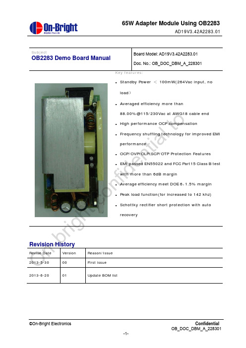
OB2283 Demo Board Manual(A)_天晖_130911
5 Thermal Test........................................................................................................................................ 20 6 Other important waveform ................................................................................................................. 20 6.1 CS, FB, Vdd & Vds waveform at no load/full load...................................................................... 20 6.2 Vds and Secondary diode waveform at full load, start/normal/output short ............................... 21 6.2.1 Vds and Secondary diode at full load, start/normal/output short ............................................ 21 6.2.2 Vds at full load, start waveform ............................................................................................... 21 6.2.3 Vds and Secondary diode at full load, normal waveform........................................................ 22 6.2.4 Vds and Secondary diode at full load, output short waveform................................................ 22
MAXHUB产品深度技术培训

小程序 – 投票器
生成选项
生成二维码
扫码投票
统计结果
小程序 – 投票器
优点: 无需连接同一局域网
缺点: 选项仅有10个 问题点: 扫码无法生成投票页面 – 检查网络 (PC)无法插入白板 – 安装最新版白板程序 (Android)无法插入白板 – 副版本更新到最新
小程序 – 便笺
优点:无限叠加,放PPT的时候比较好用
声音质量差、回响严重或爆音 – 检测 麦克风,若麦克风有问题需要返厂
小程序 – 搜索
键入内容 点击搜索按钮
浏览器打开 截屏
打开后导入白板
白板
1.手写 2.电磁笔(压感,双色
) 3.擦除 4.选择 5.撤销重做 6.加减页 7.保存 8.扫码分享 9.邮件 10.更换背景 11.插入图片 12.二次编辑13.关闭
对比:
1.PC有摄像头按钮
Android有语音拍照按钮
2.PC拍照后会即时回看拍出来的图片,再保存水平翻转的图片
Android拍照后没有即时回看,直接保存水平翻转的图片
问题点: 1.切换按钮 只是切换UI的位置,不是切换摄像头 2.PC直接点击摄像头按钮切换摄像头
安卓进入设置-设备管理切换摄像头,并且在隐私设置开放权限
T.HV510.73C
PW.400W2.751D(65/75) PW.500W2.751C(86)
电容+电磁
MT21/SA05 8M X 2 不可拆 矩阵麦 不可拆 65 75 86
产品介绍-差异对比
差异项
标准+版
外框
可拆
触摸框 可拆
摄像头模组 无
麦克风模组 无
USB板 可拆
按键板 可拆
AC1810使用手册
定时器通道0,TD0
DH
定时器通道1,TD1
FH
定时器初始化,TCNRL
附:常用的IO操作命令:
读:
MSC:i=inp(adr), i=inpw(adr) (16BIT I/O )
TC: i=inportB(adr) i=inportw(adr) (16bit I/O)
VB DLL i=vbinp(adr) i=vbinpw(adr)
AC1810的二种启动模式下,RUN的作用:
1.AC1810在软件启动模式时,启动后AC1810开始运行。
2.AC1810在外部触发模式时,启动后在外部触发有效(上升边沿输入到来)后,AC1810开始采样
2H 16位读,功能:读取FIFO中的数据,16位IO操作。
当检测到FIFO半满或AC1810中断有效时,用户一次将FIFO中的512个16BIT采样数据读走。
2-1: S1 I/O
S1-6位跳线选择器是AC1810的I/O地址选择跳线器,位于AC1810板的中下部分。AC1810占用4位A0-A3地址线, I/O译码由A4-A9,6位决定,AC1810的I/O空间为100H-3FFH。S1按二进制方法定,S1的1号跳线位置对应选择地址A4,.......,6号对应A9。S1的相应位为“跳线器短路-表示为“X””时,对应选择相应位为“0”,“开路-表示为“-””时对应选择相应位为“1”。S2的选择方式如下,S1的设置地址为300H。
注:FIFO数据传输方式是指:
FIFO为先进先出存储器,AD顺序写入数据,用户可以同时顺序将数据实时的读出。FIFO通常应用的标志位为:“半满-HF”(对AC1810的!K FIFO指FIFO存入512点时,HF=0),与“溢出-FF”(即AD已经向FIFO写入超过FIFO容量的数据)。