SK6812WWA规格书讲解
MS6818中文说明书
MS6818电缆探测仪沈阳达万科技有限公司电话:************网址:手机:139****5309邮箱:**************使用说明书USERS MANUALii iMS6818线缆探测仪目录目录 (1)介绍 (4)开箱检查 (4)安全信息 (7)1 概论 (14)1.1 产品简介 (14)1.2 MS6818电缆探测仪突出特点: (16)1.3 部件名称及功能 (17)1.3.1发射机平面视图 (17)1.3.2发射机显示界面 (18)1.3.3接收机平面图 (19)1.3.4接收机显示界面 (20)1.3.5接收机线路查找模式显示界面 (21)2 测量方法 (22)2.1 测量前的注意事项 (22)1介绍22.2 作用原理 (23)2.3 典型练习实例 (25)3 具体应用 (27)3.1 单极应用 (27)3.1.1开路式探测应用 (27)3.1.2查找和跟踪线路、插座 (28)3.1.3查找线路中断 (29)3.1.4使用两个发射机查找线路断路故障 (31)3.1.5查找电气地板供暖中的故障 (33)3.1.6查找埋设的非金属管道中的狭窄(堵塞)处 (34)3.1.7探测埋设的金属自来水管和金属供暖管道 (36)3.1.8探测同楼层供电线路 (38)3.1.9跟踪地下线路 (40)3.2 双极应用 (42)3.2.1闭合回路中的使用 (42)3.2.2查找保险丝 (43)3.2.3查找线路中的短路 (45)3.2.4探测较大埋设深度的线路 (47)3.2.5对所铺设的线路的分类或确定 (49)3.3 提高带电查找线路的有效半径的方法 (51)3.4 电网电压识别与查找线路中断 (53)MS6818线缆探测仪4 其他功能 (55)4.1 发射机的电压表功能 (55)4.2 手电筒功能 (55)4.3 背光功能 (55)4.4 静音功能 (55)4.5 自动关机功能 (55)5 技术数据 (56)5.1 发射机技术数据 (56)5.2 接收机技术数据 (57)6 维护和维修 (58)6.1 常见故障检查表 (58)6.2 发射机保险丝的检查 (59)6.3 清洁 (60)6.4 更换电池 (60)6.5 校准间隔期 (62)3介绍介绍感谢购买华仪公司设计和生产的MS6818电缆探测仪。
6812中文资料

DABiC-IV , 20-BIT SERIAL-INPUT,LATCHED SOURCE DRIVERData Sheet 26182.126AThe A6812– devices combine a 20-bit CMOS shift register,accompanying data latches and control circuitry with bipolar sourcing outputs and pnp active pull downs. Designed primarily to drivevacuum-fluorescent displays, the 60 V and -40 mA output ratings also allow these devices to be used in many other peripheral power driver applications. The A6812– features an increased data input rate (com-pared with the older UCN/UCQ5812-F) and a controlled output slew rate.The CMOS shift register and latches allow direct interfacing with microprocessor-based systems. With a 3.3 V or 5 V logic supply, they will operate to at least 10 MHz.A CMOS serial data output permits cascade connections in applica-tions requiring additional drive lines. Similar devices are available as the A6809– and A6810– (10 bits), A6811– (12 bits), and A6818– (32bits).The A6812– output source drivers are npn Darlingtons, capable of sourcing up to 40 mA. The controlled output slew rate reduces electro-magnetic noise, which is an important consideration in systems that include telecommunications and/or microprocessors and to meetgovernment emissions regulations. For inter-digit blanking, all output drivers can be disabled and all sink drivers turned on with a BLANK-ING input high. The pnp active pull-downs will sink at least 2.5 mA.Two temperature ranges are available for optimum performance in commercial (suffix S-) or industrial (suffix E-) applications. Package styles are provided for through-hole DIP (suffix -A), surface-mount SOIC (suffix -LW), or minimum-area surface-mount PLCC (suffix -EP). Copper lead frames, low logic-power dissipation, and lowoutput-saturation voltages allow these drivers to source 25 mA from all outputs continuously to more than +43°C (suffix -LW), +61°C (suffix -EP), or +77°C (suffix -A).FEATURESI Controlled Output Slew Rate I High-Speed Data Storage I 60 V Minimum Output Breakdown I High Data Input Rate I PNP Active Pull-Downs Complete part number includes a suffix to identify operating temperature range (E- or S-) and package type (-A, -EP, or -LW).Always order by complete part number, e.g., A6812SLW .6812I Low Output-Saturation Voltages I Low-Power CMOS Logic and Latches I Improved Replacements for TL5812–, UCN5812–,and UCQ5812–681220-BIT SERIAL-INPUT,LATCHED SOURCE DRIVER115 Northeast Cutoff, Box 15036Worcester, Massachusetts 01615-0036 (508) 853-5000A6812xEPA6812xLWLOAD SUPPLY OUT 2OUT 7OUT 8Dwg. PP-029-8OUT 19OUT 18OUT13SERIAL DATA OUTBLANKINGLOGICSUPPLY STROBE GROUNDCLOCKOUT 9OUT 10OUT 12OUT 11SERIAL DATA IN OUT 6OUT 1OUT 4OUT 3OUT 20OUT 5OUT 17OUT 16OUT 15OUT 14TYPICAL INPUT CIRCUITDwg. EP-010-5INDwg. PP-059-1O U T 10O U T 20O U T 11O U T 19C L O C KS E R I A L D A T A O U TL O A D S U P P L YS E R I A L D A T A I NS T R O B EG R O U N DL O G I C S U P P L Y B L A N K I N GO U T 9O U T 1OUT2OUT 8OUT 18OUT 1250751001251502.50.50A L L O W A B L E P A C K A G E P O W E R D I S S I P A T I O N I N W A T T SAMBIENT TEMPERATURE IN °C2.01.51.025Dwg. GP-024-2S UF F I X 'L W ', R = 66°C /WθJ AS UF F I X 'E P ', R =55°C /W θJ A S UF F I X 'A ', R = 45°C /W θJ A NCopyright © 2000, Allegro MicroSystems, Inc.681220-BIT SERIAL-INPUT,LATCHED SOURCE DRIVERTRUTH TABLEL = Low Logic Level H = High Logic Level X = Irrelevant P = Present State R = Previous StateLATCHES681220-BIT SERIAL-INPUT,LATCHED SOURCE DRIVER115 Northeast Cutoff, Box 15036Worcester, Massachusetts 01615-0036 (508) 853-5000ELECTRICAL CHARACTERISTICS at T A = +25°C (A6812S-) or over operating temperature range (A6812E-), V BB = 60 V unless otherwise noted.Limits @ V DD = 3.3 V Limits @ V DD = 5 VCharacteristicSymbol Test Conditions Mln.Typ.Max.Min.Typ.Max.Units Output Leakage Current I CEX V OUT = 0 V —<-0.1-15—<-0.1-15µA Output VoltageV OUT(1)I OUT = -25 mA 57.558.3—57.558.3—V V OUT(0)I OUT = 1 mA — 1.0 1.5— 1.0 1.5V Output Pull-Down Current I OUT(0)V OUT = 5 V to V BB2.5 5.0— 2.5 5.0—mA Input VoltageV IN(1) 2.2—— 3.3——V V IN(0)—— 1.1—— 1.7V Input CurrentI IN(1)V IN = V DD —<0.01 1.0—<0.01 1.0µA I IN(0)V IN = 0 V —<-0.01-1.0—<-0.01-1.0µA Input Clamp Voltage V IK I IN = -200 µA —-0.8-1.5—-0.8-1.5V Serial Data Output VoltageV OUT(1)I OUT = -200 µA 2.8 3.05— 4.5 4.75—V V OUT(0)I OUT = 200 µA —0.150.3—0.150.3V Maximum Clock Frequency f c 10*——10*——MHz Logic Supply CurrentI DD(1)All Outputs High —0.250.75—0.3 1.0mA I DD(0)All Outputs Low—0.250.75—0.3 1.0mA Load Supply CurrentI BB(1)All Outputs High, No Load — 3.0 6.0— 3.0 6.0mA I BB(0)All Outputs Low —0.220—0.220µA Blanking -to-Output Delayt dis(BQ)C L = 30 pF, 50% to 50%—0.7 2.0—0.7 2.0µs t en(BQ)C L = 30 pF, 50% to 50%— 1.8 3.0— 1.8 3.0µs Strobe -to-Output Delayt p(STH-QL)R L = 2.3 k Ω, C L ≤ 30 pF —0.7 2.0—0.7 2.0µs t p(STH-QH)R L = 2.3 k Ω, C L ≤ 30 pF — 1.8 3.0— 1.8 3.0µs Output Fall Time t f R L = 2.3 k Ω, C L ≤ 30 pF 2.4—12 2.4—12µs Output Rise Time t r R L = 2.3 k Ω, C L ≤ 30 pF 2.4—12 2.4—12µs Output Slew RatedV/dtR L = 2.3 k Ω, C L ≤ 30 pF 4.0—20 4.0—20V/µs Clock -to-Serial Data Out Delay t p(CH-SQX)I OUT = ±200 µA —50——50—nsNegative current is defined as coming out of (sourcing) the specified device terminal.Typical data is is for design information only and is at T A = +25°C.* Operation at a clock frequency greater than the specified minimum is possible but not warranteed.6812 20-BIT SERIAL-INPUT, LATCHED SOURCE DRIVER TIMING REQUIREMENTS and SPECIFICATIONS (Logic Levels are V DD and Ground)Serial Data present at the input is transferred to the shift register on the logic “0” to logic “1” transition of the CLOCK input pulse. On succeeding CLOCK pulses, the registers shift data information towards the SERIAL DATA OUTPUT. The SERIAL DATA must appear at the input prior to the rising edge of the CLOCK input waveform.Information present at any register is transferred to the respective latch when the STROBE is high (serial-to-parallel conversion). The latches will continue to accept new data as long as the STROBE is held high. Applications where the latches are bypassed (STROBE tied high) will require that the BLANKING input be high during serial data entry.When the BLANKING input is high, the output source drivers are disabled (OFF); the pnp active pull-down sink drivers are ON. The information stored in the latches is not affected by the BLANKING input. With the BLANKING input low, the outputs are controlled by the state of their respective latches.OUTDwg. WP-029OUTDwg. WP-030A. Data Active Time Before Clock Pulse(Data Set-Up Time), t su(D)...................................... 25 nsB. Data Active Time After Clock Pulse(Data Hold Time), t h(D)............................................ 25 nsC. Clock Pulse Width, t w(CH)............................................ 50 nsD. Time Between Clock Activation and Strobe, t su(C).... 100 nsE. Strobe Pulse Width, t w(STH).......................................... 50 nsNOTE – Timing is representative of a 10 MHz clock. Higherspeeds may be attainable with increased supply voltage;operation at high temperatures will reduce the specifiedmaximum clock frequency.681220-BIT SERIAL-INPUT,LATCHED SOURCE DRIVER115 Northeast Cutoff, Box 15036Worcester, Massachusetts 01615-0036 (508) 853-5000A6812EA & A6812SADimensions in Inches (controlling dimensions)Dimensions in Millimeters (for reference only)NOTES:1.Exact body and lead configuration at vendor ’s option within limits shown.2.Lead spacing tolerance is non-cumulative.3.Lead thickness is measured at seating plane or below.4.Supplied in standard sticks/tubes of 12 devices.123Dwg. MA-003-28 in144123Dwg. MA-003-28 mm144681220-BIT SERIAL-INPUT,LATCHED SOURCE DRIVERA6812EEP & A6812SEP(add “TR” to part number for tape and reel)Dimensions in Inches (controlling dimensions)NOTES:1.Exact body and lead configuration at vendor ’s option within limits shown.2.Lead spacing tolerance is non-cumulative.3.Supplied in standard sticks/tubes of 38 devices or add “TR ” to part number for tape and reel.Dwg. MA-005-28A inDwg. MA-005-28A mmDimensions in Millimeters (for reference only))681220-BIT SERIAL-INPUT,LATCHED SOURCE DRIVER115 Northeast Cutoff, Box 15036Worcester, Massachusetts 01615-0036 (508) 853-5000A6812ELW & A6812SLW(add “TR” to part number for tape and reel)Dimensions in Inches (for reference only)Dimensions in Millimeters (controlling dimensions)NOTES:1.Exact body and lead configuration at vendor ’s option within limits shown.2.Lead spacing tolerance is non-cumulative.3.Supplied in standard sticks/tubes of 27 devices or add “TR ” to part number for tape and reel.0°TO 8°Dwg. MA-008-28A inBSC0.01250.00910.0500.0160.4190.3946812 20-BIT SERIAL-INPUT, LATCHED SOURCE DRIVERThe products described here are manufactured under one or more U.S. patents or U.S. patents pending.Allegro MicroSystems, Inc. reserves the right to make, from time to time, such departures from the detail specifications as may be required to permit improvements in the performance, reliability, or manufacturability of its products. Before placing an order, the user is cautioned to verify that the information being relied upon is current.Allegro products are not authorized for use as critical components in life-support devices or systems without express written approval.The information included herein is believed to be accurate and reliable. However, Allegro MicroSystems, Inc. assumes no responsi-bility for its use; nor for any infringement of patents or other rights of third parties which may result from its use.681220-BIT SERIAL-INPUT,LATCHED SOURCE DRIVER115 Northeast Cutoff, Box 15036Worcester, Massachusetts 01615-0036 (508) 853-5000POWERINTERFACE DRIVERSFunctionOutput Ratings*Part Number †SERIAL-INPUT LATCHED DRIVERS8-Bit (saturated drivers)-120 mA 50 V‡58958-Bit 350 mA 50 V 58218-Bit 350 mA 80 V 58228-Bit 350 mA 50 V‡58418-Bit350 mA 80 V‡58428-Bit (constant-current LED driver)75 mA 17 V 62758-Bit (DMOS drivers)250 mA 50 V 65958-Bit (DMOS drivers)350 mA 50 V‡6A5958-Bit (DMOS drivers)100 mA 50 V 6B59510-Bit (active pull-downs)-25 mA 60 V 5810-F and 6809/1012-Bit (active pull-downs)-25 mA 60 V 5811 and 681116-Bit (constant-current LED driver)75 mA 17 V 627620-Bit (active pull-downs)-25 mA 60 V 5812-F and 681232-Bit (active pull-downs)-25 mA 60 V 5818-F and 681832-Bit100 mA 30 V 583332-Bit (saturated drivers)100 mA 40 V 5832PARALLEL-INPUT LATCHED DRIVERS4-Bit350 mA 50 V‡58008-Bit -25 mA 60 V 58158-Bit350 mA 50 V‡58018-Bit (DMOS drivers)100 mA 50 V 6B2738-Bit (DMOS drivers)250 mA 50 V 6273SPECIAL-PURPOSE DEVICESUnipolar Stepper Motor Translator/Driver 1.25 A 50 V‡5804Addressable 8-Bit Decoder/DMOS Driver 250 mA 50 V 6259Addressable 8-Bit Decoder/DMOS Driver 350 mA 50 V‡6A259Addressable 8-Bit Decoder/DMOS Driver 100 mA 50 V 6B259Addressable 28-Line Decoder/Driver 450 mA30 V6817*Current is maximum specified test condition, voltage is maximum rating. See specification for sustaining voltage limits.Negative current is defined as coming out of (sourcing) the output.†Complete part number includes additional characters to indicate operating temperature range and package style.‡Internal transient-suppression diodes included for inductive-load protection.。
SK6812 preliminary

深圳市阶新科技有限公司Shenzhen New Technology Co.,Ltd.SK6812Technical Data Sheet Product OverviewSK6812 is a set of smart control circuit and a light emitting circuit in one of the controlled LED source. The outer type is the same with a 5050LED chip, each element is a pixel. Pixels contained within the intelligent digital interface data latch signal shaping amplification circuit,power supply circuit, a built-in constant current circuit, high precision RC oscillator, the output is driven by the patented PWM technology,effectively guarantee the pixels in the color of the light high consistency.Data protocol using unipolar NRZ communication mode, the pixel is reset after the end of DIN, accept the data transmitted from the controller to the 24bit, the first to send data by the first pixel to pixel extraction, internal data latch, the remaining data after the internal plastic the processing circuit after shaping amplification through the DO port output began to turn to the next cascade of pixels, each pixel through a transmission signal, reduce. Pixel using automatic shaping forwarding technology, makes the number of cascade without signal transmission limit of the pixel, only limited signal transmission speed.The LED has a low driving voltage, environmental protection and energy saving, high brightness, scattering angle, good consistency, low power,long life and so on. The control circuit is integrated in the LED above,more simple circuit, small volume, easy installation.Main Application Field:•Full color LED string light, LED full color module, LED super hard and soft lights, LED guardrail tube, LED appearance / scene lighting•LED point light, LED pixel screen, LED shaped screen, a variety of electronic products, electrical equipment etc..1 / 7 Document No.: SPC / SK6812 Rev. No.: 01 SK6812Technical Data Sheet Description:•Top SMD internal integrated high quality external control line serial cascade constant current IC;•control circuit and the RGB chip in SMD 5050 components, to form a complete control of pixel, color mixing uniformity and consistency;•built-in data shaping circuit, a pixel signal is received after wave shaping and output waveform distortion will not guarantee a line;•The built-in power on reset and reset circuit, the power does not work;• gray level adjusting circuit (256 level gray scale adjustable);•red drive special treatment, color balance;•line data transmission;•plastic forward strengthening technology, the transmission distance between two points over 10M;•data transmission frequency up to 800Kbps, when the refresh rate of 30 frames per second, a cascade of not less than 1024;•built-in powerpolarity protection module, powerpolarity will not damage. Mechanical Product Size (unit mm):2 / 7 Document No.: SPC / SK6812 Rev. No.: 01SK6812Technical Data SheetMechanical Size and Pin Map (unit mm):Pin Function:Item Symbol Pin Name Function description 1 VSS Ground The signal and power supply andgrounding2 DIN Data Input Control signal input data3 VDD Power power supply pin 4DOUTData Outputcontrol signal output dataThe electrical parameters (limit parameters, Ta=25 C, VSS=0V):Parameter Symbol Range Unit Input voltage V IN+5~+24 VLogic input voltage V I-0.5~VDD+5.5 -0.5~VDD+5.5 Working temperature Topt-40~+85℃ StoragetemperatureTstg-50~+150℃EST pressure V ESD4K V3 / 7 Document No.: SPC / SK6812 Rev. No.: 01 SK6812Technical Data Sheet The electrical parameters (such as no special instructions, TA=-20 - +70 - 5.5V C, VDD=4.5, VSS=0V):Parmeter Symbol Min Typical Max Unit Test conditions The chip supplyvoltageVDD— 5.2V—R/G/B port pressure VDS,MAX......26V...DOUT drive capability IDOH...49...mADOUT conectground, themaximumdrive current IDOL...-50...mADOUT conect+, the largestcurrentThe signal input flip threshold VIH — 3.4 —VDD=5.0V VIL — 1.6 —The frequencyof PWMFPWM ... 1.2 —KHZ —Static powerconsumptionIDD ... 1 ... mA —The dynamic parameters (Ta=25 C):Parameter SymbolMinTypicalMax Unit Test conditionsThe speed ofdata transmission fDIN—800...KHZThe duty ratio of67% (data 1)DOUT T PLZ——500ns DIN—>DOUTtransmissiondelayT PLZ — ... 500 ns4 / 7 Document No.: SPC / SK6812 Rev. No.: 01SK6812Technical Data SheetRGB chip characteristic parameters:Color Wavelength(nm) Luminous intensity(mcd) Working voltage(v) Red 620-625 700-1000 2.0-2.2 Green 522.5-525 1500-2200 3.0-3.3 Blue467.5-470700-10003.0-3.3The data transmission time (TH+TL=1.25µs±600ns):TOH 0 code, high level time0.3µs ±0.15µs T1H 1 code, high level time0.6µs +0.15µs TOL 0 code, low level time0.9µs ±0.15µs TIL 1 code, low level time0.6µs +0.15µs TrstReset code, low level time80µs5 / 7 Document No.: SPC / SK6812 Rev. No.: 01SK6812Technical Data Sheet Timing waveform:Input code: Connection mode:The method of data transmission:Note: the D1 sends data for MCU, D2, D3, D4 for data forwarding automatic shaping cascade circuit.The data structure of 24bit:G7 G6 G5 G4 G3 G2 G1 G0 R7 R6 R5 R4R3 R2 R1 R0 B7 B6 B5 B4 B3 B2 B1 B0 Note: high starting, in order to send data (G7 - G6 - ...... ..B0)6 /7 Document No.: SPC / SK6812 Rev. No.: 01 SK6812Technical Data Sheet The typical application circuit:7 / 7 Document No.: SPC / SK6812 Rev. No.: 01。
开关电源参数规格的定义与判定

产品有输出短路保护功能 (设计时短路输入功率参考判定标准)
判定符合标准
Pout≤30W; 短路时输入功率≤5W
备注
输入功率为跳动时,取最大与 最小输入功率的平均值(温升 30W<Pout≤60W; 短路时输入功率≤8W 符合安规标准和元件应力满足 60W<Pout; 短路时输入功率≤12W 应力标准).
11>. 输出过流保护
规格定义
产品有输出过流保护功能,过载过程中变 压器不应有饱和现象,温度应符合安规要 求,MOS/肖特基的电流与电压应力不可超 出规格值的100%.(输出电流<2A时,OCP需 在1.2-2.0倍额定输出负载;输出电流≥ 2A时,OCP点需满足规格值+0.5A以上到额 定负载的1.8倍范围).
备注
需满足>±0.2KV以上为合格依 据(极限测试)
28>. EFT
规格定义
Line to Neutral: ±1KV
判定符合标准
Line to Neutral: ±1KV以上为合格.
备注
29>. MTBF
规格定义
≥50000Hrs(25℃) (MIL-STD-217F)
判定符合标准
≥80000Hrs
备注
30>. 元件应力
1. DIODE:
额定电压(最大值)
额定电流(平均值) 50% 50% 50% 50% 额定电流(平均值) 50% 额定电流 额定电流 50% 50% 50%
额定规格 150℃ 125℃ 150℃ 150℃ 额定规格 150℃ 105℃ 100℃ 150℃ 130℃ 130℃
40℃操作环境允许值 120℃ 110℃ 120℃ 125℃ 40℃操作环境允许值 120℃ 90℃ 100℃ 120℃ 40℃操作环境允许值 110℃ 110℃ 40℃操作环境允许值 100℃ 120/80℃ 95℃ 100℃ 40℃操作环境允许值 120℃ 120℃ 100℃ 120℃
GT-S6812i中文说明书
7
入门指南
包装内容
检查产品包装盒中是否有以下物品: • 设备 • 电池 • 快速入门指南 只可使用经过三星认可的软件。盗版或非法软件可能会导致损坏或故障,此 情形不在保修范围内。 • 设备随附的物品和可用配件可能会因所在地区或服务提供商而异。 • 随附的物品专为本设备设计,可能与其他设备并不兼容。 • 外观和规格如有变更,恕不另行通知。 • 可以向本地三星零售商购买其他配件。购买前请确保它们与设备兼容。 • 其他配件可能与您的设备并不兼容。 • 只可使用经过三星许可的配件。使用未经许可的配件所造成的故障不属 保修服务范畴。 • 是否提供所有配件完全取决于制造公司。有关可用配件的更多信息,请 参阅三星网站。
59 视频播放器
应用程序
60 Samsung Apps 61 游戏圈 61 悦读圈 61 影视圈
实用程序
62 备忘录 63 S日历 64 Quickoffice 65 时钟 67 计算器 67 词典 68 录音机 69 搜索 70 我的文件 70 下载文件
旅行和本地资讯
71 高德地图
设定
72 关于设定 72 WLAN 73 蓝牙 73 数据使用 74 更多设置
GT-S6812i
使用说明书
/cn
关于本说明书
本设备采用三星的高科技和高标准,旨在提供优质的移动通信和娱乐体验。本使用 说明书专门用于详细介绍设备的功能与特性。
• 使用本设备之前,请先阅读本说明书,以确保安全和正确使用。 • 说明基于设备的默认设置。 • 图像和屏幕截图可能与实际产品的外观不同。 • 内容可能与最终产品不同,也可能与服务提供商或运营商提供的软件不
调整音量
向上或向下按下音量键以调整铃声音量,或在播放音乐或视频时调整音量。
K.2系列产品用户手册说明书
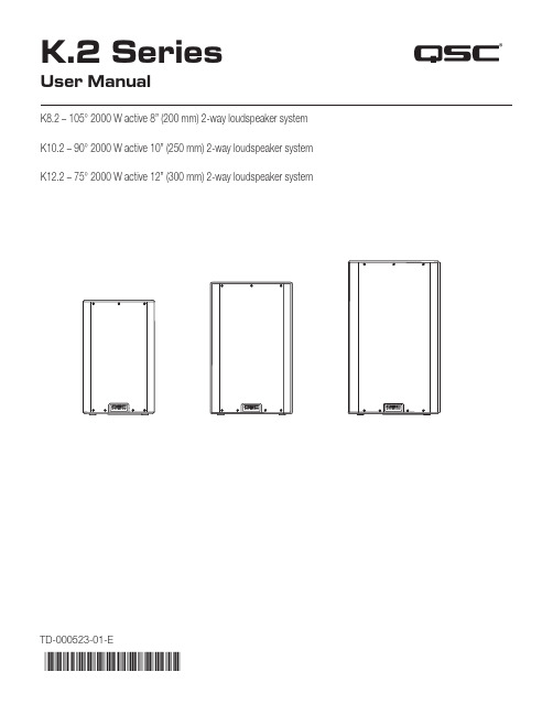
K.2 Series®User ManualK8.2 – 105° 2000 W active 8” (200 mm) 2-way loudspeaker systemK10.2 – 90° 2000 W active 10” (250 mm) 2-way loudspeaker systemK12.2 – 75° 2000 W active 12” (300 mm) 2-way loudspeaker systemTD-000523-01-E*TD-000523-01*EXPLANATION OF SYMBOLSThe term “WARNING!” indicates instructions regarding personal safety. If the instructions are not followed the result may be bodily injury or death.The term “CAUTION!” indicates instructions regarding possible damage to physical equipment. If these instructions are not followed, it may result in damage to the equipment that may not be covered under the warranty.The term “IMPORTANT!” indicates instructions or information that are vital to the successful completion of the procedure. The term “NOTE” is used to indicate additional useful information.NOTE: The intent of the lightning flash with arrowhead symbol in a triangle is to alert the user to the presence of un-insulated “dangerous” voltage within the product’s enclosure that may be of sufficient magnitude toconstitute a risk of electric shock to humans.NOTE: The intent of the exclamation point within an equilateral triangle is to alert the user to the presence of important safety, and operating and maintenance instructions in this manual.IMPORTANT SAFETY INSTRUCTIONSWARNING!: TO PREVENT FIRE OR ELECTRIC SHOCK, DO NOT EXPOSE THIS EQUIPMENT TO RAIN OR MOISTURE. DO NOT USE THIS APPARATUS NEAR WATER.1. Read these instructions.2. Keep these instructions.3. Heed all warnings.4. Follow all instructions.5. Do not use this apparatus near water.6. Clean only with a dry cloth.7. Do not block any ventilation opening. Install in accordance with the manufacturer’s instructions.8. Do not install near any heat sources such as radiators, heat registers, stoves, or other apparatus (including amplifiers)that produce heat.9. Do not defeat the safety purpose of the polarized or grounding-type plug. A polarized plug has two blades with onewider than the other. A grounding type plug has two blades and a third grounding prong. The wide blade or the third prong are provided for your safety. If the provided plug does not fit into your outlet, consult an electrician for replacement of the obsolete outlet.10. Protect the power cord from being walked on or pinched particularly at plugs, convenience receptacles, and the pointwhere they exit from the apparatus.11. Only use attachments/accessories specified by the manufacturer.12. Unplug this apparatus during lightning storms or when unused for long periods of time.13. Refer all servicing to qualified service personnel. Servicing is required when the apparatus has been damaged in anyway, such as power-supply cord or plug is damaged, liquid has been spilled or objects have fallen into the apparatus, the apparatus has been exposed to rain or moisture, does not operate normally, or has been dropped.14. The appliance coupler, or the AC Mains plug, is the AC mains disconnect device and shall remain readily operableafter installation.15. Adhere to all applicable, local codes.16. To prevent electrical shock, the power cord shall be connected to a mains socket outlet with a protective earthing connection.17. Consult a licensed, professional engineer when any doubt or questions arise regarding a physical equipment installation.18. Do not use any aerosol spray, cleaner, disinfectant or fumigant on, near or into the apparatus. Clean only with a dry cloth.19. Do not unplug the unit by pulling on the cord, use the plug.20. Do not submerge the apparatus in water or liquids.21. Keep ventilation opening free of dust or other matter.WarrantyFor a copy of the QSC Limited Warranty, visit the QSC website at Maintenance and RepairWARNING!: Advanced technology, e.g., the use of modern materials and powerful electronics, requires speciallyadapted maintenance and repair methods. To avoid a danger of subsequent damage to the apparatus, injuries to personsand/or the creation of additional safety hazards, all maintenance or repair work on the apparatus should be performed only by a QSC authorized service station or an authorized QSC International Distributor. QSC is not responsible for any injury,harm or related damages arising from any failure of the customer, owner or user of the apparatus to facilitate those repairs. Life Cycle: 10 years, Storage Temperature range: -20C to +70C, Relative Humidity range: 5 - 85% RHFCC StatementNOTE: This equipment has been tested and found to comply with the limits for a Class B digital device,pursuant to Part 15 of the FCC Rules.These limits are designed to provide reasonable protection against harmful interference in a residential installation. This equipment generates, uses and can radiate radio frequency energy and, if not installed and used in accordance with the instructions, may cause harmful interference to radio communications. However, there is no guarantee that interference will not occur in a particular installation. If this equipment does cause harmful interference to radio or television reception, which can be determined by turning the equipment off and on, the user is encouraged to try to correct the interference by one or more of the following measures:• Reorient or relocate the receiving antenna.• Increase the separation between the equipment and receiver.• Connect the equipment into an outlet on a circuit different from that to which the receiver is connected.• Consult the dealer or an experienced radio/TV technician for help.RoHS StatementsThese products are in compliance with European Directive 2011/65/EU – Restriction of Hazardous Substances (RoHS). These products are in compliance with “China RoHS” directives per GB/T26572. The following table is provided for product use in China and its territories:These products 这些产品部件名称(Part Name)有害物质(Hazardous Substances)铅(Pb)汞(Hg)镉(Cd)六价铬(Cr(vi))多溴联苯(PBB)多溴二苯醚(PBDE)电路板组件(PCB Assemblies)X O O O O O机壳装配件(Chassis Assemblies)X O O O O O本表格依据 SJ/T 11364 的规定编制。
XT1511 SK6812 WS2812B灯珠使用规格书,操作说明书
1.目的Purpose:内置IC-LED系列LED灯头表面使用的是高硬度的硅树脂,能够确保客户使用环氧树脂,PU胶,硅胶滴胶加工时都不会死灯,也有非常好的抗硫化能力。
和支架的兼容性也非常好,但是硅树脂对湿度和除湿处理要求非常高,在潮湿季节使用时需要非常注意,确保生产的安全性。
2.运输及适用范围:所有内置IC-LED系列产品在运输过程中,需保持正面朝上,防潮防水,运输过程中逼免挤压、碰撞和剧烈震动。
3.产品储存及期限:室温密封存储:20℃~30℃,40%~60%RH,产品有效期为3个月;防潮密封存储:20℃~30℃,25%~60%RH,产品有效期为6个月;产品拆包开封后,建议1 小时内使用完成,(环境条件温度<30℃,湿度<60%)。
4.除湿处理LED 产品超出以上规定期限,或者由于其他原因受潮,建议客户做除湿处理后再使用。
除湿方法:70℃-75℃/22±2 小时。
5.静电防护LED 是静电敏感器件,虽然LED 产品具有优异的抗静电能力,但每经历一次静电释放产生的冲击,都会对LED 造成一定程度的损坏。
因而在使用LED 产品过程中需要做好静电防护措施,例如佩戴防静电手套及防静电手环等。
6.手动焊接操作指引建议使用功率不超过30W 的电烙铁,控制电烙铁温度不高于380℃,每次焊接时电烙铁在支架引脚上停留时间不超过3秒,如需要反复焊接时,间隔停留时间不少于2秒,避免长时间高温对L ED 造成损伤。
焊接过程中,请勿触摸或挤压LED 的表面,避免对L ED 内部造成损伤,同时请注意避免电烙铁对LED 表面胶体的烫伤及其它损伤。
7.回流焊指引回流焊相关参数设定,请参考下图及下表,推荐使用千住、阿尔法、汉高乐泰等品牌焊锡膏,建议客户根据所采用的焊锡材料供应商提供的材料特性基础上进行必要的调整。
8.生产注意事项1. 所有产品,在贴片时,请仔细检查,若真空包装完好无损,无漏气现象,请直接使用,可以不用烘烤除湿处理。
国光CJ6812系列液晶显示终端用户指南
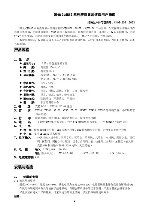
国光CJ6812系列液晶显示终端用户指南终端生产许可证编号:XK09-204 2023 国光CJ6812系列液晶显示终端主要有CJ6812L、6812L+ 、CJ6812A+ 三种型号,全兼容国光终端及国内其他主要终端,支持通信加密、BIOS在线下载等功能。
具有独立的六串一并接口,10M以太网接口,支持XT/AT方式键盘,支持多进程或多主机和8个虚拟屏幕。
一体化外形结构,内置电源。
本指南的知识产权属江苏国光信息产业股份有限公司所有,未经许可不得复制。
内容如有修改,恕不另行通知。
1、显示◆显示尺寸:12英寸彩色液晶显示屏◆亮度:典型值 100cd/m2◆对比度:典型值18:1◆显示规格:西文80 x 26行,7×12点阵中文40 x 26行,15×16点阵◆字符颜色:白字、绿字◆底色颜色:黑底、兰底◆字符属性:正常、闪烁、反视、下划、右直、保密等◆显示字形:正常、倍高、倍宽、倍高倍宽◆滚动方式:跳跃滚动、平滑滚动、不滚动◆图形:丰富的图形命令2、键盘支持PC101、VT220、PC104键盘3、仿真VT320、VT200、VT100、VT52、CT100、XENIX、TV925、VT382等终端类型,可扩展其它仿真类型。
4、打印屏幕打印、拷贝打印、直接透明打印、间接透明打印5、通讯一个CENTRONICS并行接口,六个EIA-RS232C串行接口,一个10BASE-T网络接口6、文字◆西文:标准ASCⅡ字符集、DEC技术字符集、DEC特殊图形字符集、六种多国半角字符集◆中文:支持GB18030国家标准7、汉字输入一次性装入拼音码、五笔字型、五笔划、笔型码、八笔划、电报码、图形副盘、国标码、区位码、国标字符、短语、汉字、首尾码二套、快速码二套共计16种汉字输入法,支持GBK拼音输入和GB18030内码、大五笔输入8、电源输入:220V±10% ≤0.15A输出(供外设用): +5V (≤0.5A) +12V (≤0.3A) -12V (≤0.1A)9、电磁兼容性A级1、终端的安装1.1 安装环境要求温度5℃~40℃,湿度40%~90%,额定电压为交流220V±10%,电源系统要求配有交流稳压器或UPS。
- 1、下载文档前请自行甄别文档内容的完整性,平台不提供额外的编辑、内容补充、找答案等附加服务。
- 2、"仅部分预览"的文档,不可在线预览部分如存在完整性等问题,可反馈申请退款(可完整预览的文档不适用该条件!)。
- 3、如文档侵犯您的权益,请联系客服反馈,我们会尽快为您处理(人工客服工作时间:9:00-18:30)。
SK6812WWA
规格书
智能外控表面贴装SMD型LED 文件编号: SPC/ SK6812WWA
产品型号: SK6812WWA
产品描述: 5.5x5.0x1.6毫米0.2瓦特智能外控表面贴装型SMD LED
版本号.: 01
日期: 2015-06-18
智能外控表面贴装SMD型LED
型号: SK6812WWA
1.产品概述:
SK6812WWA是一个集控制电路与发光电路于一体的智能外控LED光源。
其外型与一个5050LED灯珠相同,每个元件
即为一个像素点。
像素点内部包含了智能数字接口数据锁存信号整形放大驱动电路,电源稳压电路,内置恒流电路
,高精度RC振荡器,输出驱动采用专利PWM技术,有效保证了像素点内光的颜色高一致性。
数据协议采用单极性归零码的通讯方式,像素点在上电复位以后,DIN端接受从控制器传输过来的数据,首先送过来
的24bit数据被第一个像素点提取后,送到像素点内部的数据锁存器,剩余的数据经过内部整形处理电路整形放大后
通过DO端口开始转发输出给下一个级联的像素点,每经过一个像素点的传输,信号减少24bit。
像素点采用自动整形
转发技术,使得该像素点的级联个数不受信号传送的限制,仅仅受限信号传输速度要求。
LED具有低电压驱动,环保节能,亮度高,散射角度大,一致性好,超低功率,超长寿命等优点。
将控制电路集成
于LED上面,电路变得更加简单,体积小,安装更加简便。
2.主要应用领域:
●LED全彩发光字灯串,LED全彩模组,LED幻彩软硬灯条,LED护栏管,LED外观/情景照明
●LED点光源,LED像素屏,LED异形屏,各种电子产品,电器设备跑马灯。
3.特性说明:
●Top SMD内部集成高质量外控单线串行级联恒流IC;
●控制电路与芯片集成在SMD 5050元器件中,构成一个完整的外控像素点,色温效果均匀且一致性高。
●内置数据整形电路,任何一个像素点收到信号后经过波形整形再输出,保证线路波形畸变不会累加。
●内置上电复位和掉电复位电路,上电不亮灯;
●灰度调节电路(256级灰度可调),
●单线数据传输,可无限级联。
●整形转发强化技术,两点间传输距离超过10M.
●数据传输频率可达800Kbps,当刷新速率30帧/秒时,级联数不小于1024点。
4.机械尺寸:
备注:
1. 以上标示单位为毫米.
2. 除非另外注明,尺寸公差为±0.1毫米.
5.引脚图及功能:
6.产品命名一般说明:
表面贴装LED采用卷盘包装,LED在用普通或防静电袋包装后再装在纸箱中. 纸箱用于保护运输途中LED不受机械冲
击,纸箱不防水,因此请注意防潮防水。
表面贴装型LED使用注意事项
1. 特点
通过这个资料,达到让欧思科光电的客户清楚地了解LED的使用方法的目的。
2. 描述
通常LED也象其它的电子元件一样有着相同的使用方法,为一让客户更好地使用欧思科光电的LED产品,请参看下面的
LED保护预防措施。
3. 注意事项
3.1. 灰尘与清洁
LED的表面是采用硅树胶封装的, 硅树脂对于LED的光学系统和抗老化性能都起到很好的保护作用. 可是, 硅树脂质柔
软, 易粘灰尘, 因此, 要保持作业环境的洁净. 当然, 在LED表面有一定限度内的尘埃, 也不会影响到发光亮度, 但我们仍
应避免尘埃落到LED表面. 打开包装袋的就优先使用, 安装过LED的组件应存放在干净的容器中等.
在LED表面需要清洁时, 如果使用三氯乙烯或者丙酮等溶液会出现使LED表面溶解等现象.
不可使用具用溶解性的溶液清洁LED, 可使用一此异丙基的溶液, 在使用任何清洁溶液之前都应确认是否会对LED有溶解
作用.
请不要用超声波的方法清洁LED,如果产品必须使用超声波,那么就要评估影响LED的一些参数,如超声波
功率,烘烤
的时间和装配的条件等,在清洁之前必须试运行,确认是否会影响到LED。
3.2. 防潮包装
将LED包装在铝膜的袋中是为了避免LED在运输和储存时吸收湿气,在包装袋中放有干燥剂,以吸收湿气如果LED吸收了
水气,那么在LED过回流焊时,水气就会蒸发而膨胀,有可能使胶体与支架脱离以及损害LED的光学系统。
由于这个原因,
防湿包装是为了使包装袋内避免有湿气。
3.3. 储存
为了避免LED吸湿,应将散装或贴过带的LED贮存在干燥箱或带有干燥剂的容器中,另外,也可在以下的环境中短时间储
存:
a. 温度: 5℃~30℃
b. 湿度: 小于60%
使用LED时,在打开铝膜静电袋以后应很快进行焊接,对于剩余的LED应再次封口包装。
打开铝膜袋子后的LED,应在1小
时内完成回流焊接。
如果需要烘烤,请参考以下的烘烤温度:
在70℃±5℃的烤箱中烘烤不少于24小时
3.4. 回流焊接
经欧思科光电采用下面所列参数检测证明,表面贴装型LED符合JEDEC J-STD-020C标准。
作为一般指导原则,欧思科光电
建议客户遵循所用焊锡膏制造商推荐使用的焊接温度曲线。
请注意此一般指导原则可能并不适用于所有PCB设计和回流焊设备的配置。
3.5. 热量的产生
对于LED产品,散热方面的设计是很重要的,在系统设计时请考虑LED所产生的热量,PCB板的热阻、LED
放置的密度和相
关组成,以及输入的电功率都会使温度增加。
因此,为避免出现过多热量的产生,须保证LED运行时要在产品规格书中所要求的最大规格范围之内。
在设定LED的驱动电
流时,应考虑到最高的环境温度。
3.6. 防静电及电涌
. 静电和电涌会伤害到LED
. 为保护好LED,无论什么时间与场合,只要接触到LED时,都要穿带防静电手带,防静电脚带及防静电手套
. 所有的装置和仪器设备均须接地
. 建议每一种产品在出货前检验时,都应有相关电性测试,以挑选出因静电而产生的不良品
. 在电路设计时,应考虑消除电涌对LED危害的可能性.
3.7. 其它
如果超出规格书以外而进行使用时,出任何问题我们都将不承担责任。
在很多的标准件上也都应用这种LED,诸如家电产品,通信设备,办公设备以及电子设备等等。
如果客户应用时有特殊的质量要求或关系到人类生活的信赖性要求时,请提前与我们商量联系,例如用医疗设备,航天设备
应用,交通信号以及安全系统等等。
必须要注意是在使用LED的驱动电路时,确保其反向电压值不超出最大额定范围。
LED可以发出很强的足以伤害到眼睛的光,要注意预防,不可过长时间用肉眼直视LED的光。
在大量使用之前,应与我们交流,了解更详细的规格要求。
LED产品形状和规格如有改变,请恕不能及时相告。