MC74HC157ADR2,MC74HC157ADR2,MC74HC157ADTR2G, 规格书,Datasheet 资料
SL74HC157中文资料

IIN ICC
Maximum Input Leakage Current Maximum Quiescent Supply Current (per Package)
VIN=VCC or GND VIN=VCC or GND IOUT=0µA
SLS
System Logic Semiconductor
Value -0.5 to +7.0 -1.5 to VCC +1.5 -0.5 to VCC +0.5 ±20 ±25 ±50 750 500 -65 to +150 260
Unit V V V mA mA mA mW °C °C
Maximum Ratings are those values beyond which damage to the device may occur. Functional operation should be restricted to the Recommended Operating Conditions. +Derating - Plastic DIP: - 10 mW/°C from 65° to 125°C SOIC Package: : - 7 mW/°C from 65° to 125°C
SLS
System Logic Semiconductor
元器件交易网
SL74HC157
DC ELECTRICAL CHARACTERISTICS (Voltages Referenced to GND)
VCC Symbol Parameter Test Conditions V Guaranteed Limit 25 °C to -55°C 1.5 3.15 4.2 0.5 1.35 1.8 1.9 4.4 5.9 3.98 5.48 0.1 0.1 0.1 0.26 0.26 ±0.1 4.0 ≤85 °C 1.5 3.15 4.2 0.5 1.35 1.8 1.9 4.4 5.9 3.84 5.34 0.1 0.1 0.1 0.33 0.33 ±1.0 40 ≤125 °C 1.5 3.15 4.2 0.5 1.35 1.8 1.9 4.4 5.9 3.7 5.2 0.1 0.1 0.1 0.4 0.4 ±1.0 160 µA µA V Unit
74VHC153MTC;74VHC153M;74VHC153MTCX;74VHC153MX;74VHC153SJ;中文规格书,Datasheet资料

74VHC153 Dual 4-Input Multiplexer74VHC153 Dual 4-Input MultiplexerLogic Symbols IEEC/IECFunctional DescriptionThe VHC153 is a dual 4-input multiplexer. It can select two bits of data from up to four sources under the control of the common Select inputs (S 0 , S 1 ). The two 4-input multi-plexer circuits have individual active-LOW Enables (E a ,E b ) which can be used to strobe the outputs indepen-dently. When the Enables (E a , E b ) are HIGH, the corre-sponding outputs (Z a , Z b ) are forced LOW. The VHC153 is the logic implementation of a 2-pole, 4-position switch,where the position of the switch is determined by the logic levels supplied to the Select inputs. The logic equations for the outputs are shown below.Z a = E a • (I 0a • S 1 • S 0 + I 1a • S 1 • S 0 + I 2a • S 1 • S 0+ I 3a • S 1 • S 0 )Z b = E b • (I 0b • S 1 • S 0 + I 1b • S 1 • S 0 + I 2b • S 1 • S 0+ I 3b • S 1 • S 0 )Truth TableH = HIGH Voltage Level L = LOW Voltage Level X = ImmaterialSelect Inputs (a or b)Output Inputs S 0S 1EI 0I 1I 2I 3ZX X H X X X X L L L L L X X X L L L L H X X X H H L L X L X X L H L L X H X X H L H L X X L X L L H L X X H X H H H L X X X L L HHLXXXHH74VHC153 Dual 4-Input Multiplexer Logic DiagramPlease note that this diagram is provided only for the understanding of logic operations and should not be used toestimate propagation delays.74VHC153 Dual 4-Input MultiplexerAbsolute Maximum RatingsStresses exceeding the absolute maximum ratings may damage the device. The device may not function or beoperable above the recommended operating conditions and stressing the parts to these levels is not recommended. In addition, extended exposure to stresses above the recommended operating conditions may affect device reliability. The absolute maximum ratings are stress ratings only.Recommended Operating Conditions (1)The Recommended Operating Conditions table defines the conditions for actual device operation. Recommended operating conditions are specified to ensure optimal performance to the datasheet specifications. Fairchild does not recommend exceeding them or designing to absolute maximum ratings.Note:1.Unused inputs must be held HIGH or LOW. They may not float.Symbol ParameterRatingV CC Supply Voltage –0.5V to +7.0V V IN DC Input Voltage –0.5V to +7.0V V OUT DC Output Voltage –0.5V to V CC + 0.5VI IK Input Diode Current –20mA I OK Output Diode Current ±20mA I OUT DC Output Current ±25mA I CC DC V CC /GND Current ±50mAT STG Storage Temperature–65°C to +150°CT LLead Temperature (Soldering, 10 seconds)260°CSymbol ParameterRatingV CC Supply Voltage 2.0V to +5.5V V IN Input Voltage 0V to +5.5V V OUT Output Voltage 0V to V CCT OPR Operating Temperature –40°C to +85°C t r , t fInput Rise and Fall Time, V CC = 3.3V ± 0.3VV CC =5.0V ± 0.5V0ns/V ∼ 100ns/V 0ns/V ∼20ns/V74VHC153 Dual 4-Input MultiplexerDC Electrical CharacteristicsAC Electrical CharacteristicsNote:2.C PD is defined as the value of the internal equivalent capacitance which is calculated from the operating currentconsumption without load. Average operating current can be obtained by the equation: I CC (opr.) = C PD • V CC • f IN + I CCSymbolParameterV CC(V)Conditions T A = 25°CT A = –40°C to+85°CUnitsMin.Typ.Max.Min.Max.V IH HIGH Level Input Voltage2.0 1.50 1.50V3.0–5.50.7 x V CC0.7 x V CCV IL LOW Level Input Voltage 2.00.500.50V3.0–5.50.3 x V CC0.3 x V CCV OHHIGH Level Output Voltage2.0V IN = V IH or V ILI OH = –50µA 1.9 2.0 1.9V 3.0 2.9 3.0 2.94.5 4.4 4.54.43.0I OH = –4mA 2.58 2.484.5I OH = –8mA3.943.80V OLLOW Level Output Voltage2.0V IN = V IH or V ILI OL = 50µA 0.00.10.1V3.00.00.10.14.50.00.10.13.0I OL = 4mA 0.360.444.5I OL = 8mA0.360.44I IN Input Leakage Current 0–5.5V IN = 5.5V or GND ±0.1±1.0µA I CCQuiescent Supply Current5.5V IN = V CC or GND4.040.0µASymbolParameterV CC (V)ConditionsT A = 25°CT A = –40°C to +85°C UnitsMin.Typ.Max.Min.Max.t PLH , t PHLPropagation Delay, I n to Z n3.3 ± 0.3C L = 15pF 7.711.9 1.014.0ns C L = 50pF 10.215.4 1.017.55.0 ± 0.5C L = 15pF 5.07.7 1.09.0ns C L = 50pF 6.59.7 1.011.0t PLH , t PHLPropagation Delay, S n to Z n3.3 ± 0.3C L = 15pF 10.816.7 1.019.5ns C L = 50pF 13.320.2 1.023.05.0 ± 0.5C L = 15pF 6.89.9 1.011.5ns C L = 50pF 8.311.9 1.013.5t PLH , t PHLPropagation Delay, E n to Z n3.3 ± 0.3C L = 15pF 6.310.1 1.012.0ns C L = 50pF 8.813.6 1.015.55.0 ± 0.5C L = 15pF 4.4 6.4 1.07.5ns C L = 50pF 5.98.4 1.09.5C IN Input Capacitance V CC = Open41010pF C PDPower Dissipation Capacitance(2)20pF74VHC153 Dual 4-Input Multiplexer The™分销商库存信息:FAIRCHILD74VHC153MTC74VHC153M74VHC153MTCX 74VHC153MX74VHC153SJ74VHC153SJX 74VHC153N。
74HC系列芯片资料

74HC00四2输入与非门 国际通用符号 54/7400 , 54/74H00, 54L 00 , 54/74S00 , 54/74LS0074LV00 , 74LVC0074HC02四2输入或非门 国际通用符号54/7402 , 54L 02 , 54/74S02 , 54/74LS02 , 54/74AS02 , 54/74ALS02 , 54/ 74F 02 , 54/74HC02 , 74AC 02 , 54/74HCT02 , 54/74ACT02 , 54/74AHC02 , 54/AHCT02 , 74LV02 , 74LVC0254/74HC00 , 54/ 74AC 00 , 54/74HCT00 54/74ACT00 , 54/74AHC0054/74AHCT00 ,54/74ALS00 , 54/ 74F 00 ,]Y 1A IB 2Y 2A 2B GND74HC04六反相器国际通用符号54/7404 , 54L 04 , 54/74H04 , 54/74S04 , 54/74LS04 , 54/74AS04 , 54/74ALS04 , 54/ 74F 04 , 54/74HCU04 , 54/74HC04 , 54/ 74AC 04 , 54/74HCT04 , 54/74ACT04 , 54/74AHC04 , 54/74AHCT04 , 74LV04 , 74LVC04 , 54/74AHCU04 , 74LVU04 , 74LVCU0474HC08四2输入与门国际通用符号54/7408 , 54/74S08 , 54/74LS08 , 54/74AS08 , 54/74ALS08 , 54/ 74F 08 , 54/74HC08 , 54/74HCT08 , 54/ 74AC08 , 54/74ACT08 , 54/74AHC08 , 54/74AHCT08 , 74LV08 , 74LVC08Y = AB74HC10三3输入与非门国际通用符号54/7410 , 54L 10 , 54/74H10 , 54/74S10 ,54/74LS10 54/74AS10 54/ 74F 10 , 54/74HC10 , 54/ 74AC 10 54/74HCT10 , 54/74ACT10 54/74ALS10 74LV101C 1Y 1C 3 日3A 3¥cP1A IB 2A 2B 2C 2Y GND 74HC20双4输入与非门国际通用符号54/7420 , 54L 20 , 54/74H20 , 54/74S20 54/ 74F 20 , 54/74HC20 , 54/ 74AC 20 ,,54/74LS20 , 54/74AS2054/74HCT20 , 54/74ACT2054/74ALS20¥ = ABCDO2YalrTHliTLir 4ID 1Y GNDV c< 2D 2C \C 2B 2A74HC30 8输入与非门国际通用符号54/7430 , 54L 30 , 54/74H30 , 54/74S30 ,54/74LS30 54/74AS30 54/74ALS30/ = ABCDEFGH.V<x NC H G NC MC Y7—L 1A B C D E F GND74HC32四2输入或门国际通用符号54/7432 , 54/74S32 , 54/74LS32 , 54/74AS32 , 54/74ALS32 , 54/ 74F 32 , 54/74HC32 ,54/ 74AC32 , 54/74HCT32, 54/74ACT32 , 54/74AHC32 , 54/74AHCT32 , 74LV32 , 74LVC32Y = A+BO74HC42 BCD —十进制译码器国际通用符号 54/ 7442A , 54L 42, 54/74LS42, 54/74HC42, 54/74HCT42十选一,在所有无效输入状态下,输出维持高电平。
74HC系列资料查询

7474HC4052 74HC4053 74HC4060 74HC4066 74HC4075 74HC42 74HC423A 74HC4514 74HC4538A 74HC4543 74HC51 74HC521 74HC533 74HC534 74HC540 74HC541 74HC58 74HC589 74HC594 74HC595 74HC597 74HC620 74HC623 74HC640 74HC643 74HC646 74HC648 74HC688 74HC7266 74HC73 74HC74A 74HC75 74HC76 74HC85 74HC86 74HC942 74HC943 74LS00 74LS02 74LS03 74LS04 74LS05 74LS08 74LS09 74LS10 74LS109 74LS11 74LS112 74LS113 74LS114 74LS122 74LS123 74LS125 74LS160 74LS136 74LS138 74LS139 74LS14 74HC147 74HC148 74HC149 74LS151 74LS153 74LS155 74LS156 74LS157 74LS158 74LS160A 74LS161A 74LS162A 74LS163A 74LS164 74LS168 74LS169 74LS173 74LS174 74LS175 74LS190 74LS191 74LS192 74LS193 74LS194A 74LS195A 74LS20 74LS21 74LS240 74LS244 74LS245 74LS253 74LS256 74LS257 74LS258 74LS27 74LS279 74LS28 74LS283 74LS30 74LS32 74LS352 74LS367 74LS368A 74LS373 74LS76 74LS379 74LS38 74LS390 74LS393 74LS42 74LS48 74LS49 74LS51 74LS540 74LS541 74LS74 74LS682 74LS684 74LS75 74LS83A 74LS85 74LS86 74LS90 74LS95B 74LS688 74LS136 4000与4500系列型号规格性能说明CD4000 "3输入双或非门1反相器"CD4001 "四2输入或非门"CD4002 "双4输入或非门"CD4006 "18级静态移位寄存器"CD4007 "双互补对加反相器"CD4008 "4位二进制并行进位全加器"CD4009 "六缓冲器/转换器(反相)"CD4010 "六缓冲器/转换器(同相)"CD40100 "32位双向静态移位寄存器"CD40101 "9位奇偶发生器/校验器"CD40102 "8位BCD可预置同步减法计数器"CD40103 "8位二进制可预置同步减法计数器"CD40104 "4位三态输出双向通用移位寄存器"CD40105 "先进先出寄存器"CD40106 "六施密特触发器"CD40107 "2输入双与非缓冲/驱动器"CD40108 "4×4多端寄存"CD40109 "四三态输出低到高电平移位器" CD4011 "四2输入与非门"CD40110 "十进制加减计数/译码/锁存/驱动" CD40117 "10线—4线BCD优先编码器"CD4012 "双4输入与非门"CD4013 "带置位/复位的双D触发器"CD4014 "8级同步并入串入/串出移位寄存器" CD40147 "10线—4线BCD优先编码器"CD4015 "双4位串入/并出移位寄存器"CD4016 "四双向开关"CD40160 "非同步复位可预置BCD计数器" CD40161 "非同步复位可预置二进制计数器" CD40162 "同步复位可预置BCD计数器"CD40163 "同步复位可预置二进制计数器" CD4017 "十进制计数器/分频器"CD40174 "六D触发器"CD40175 "四D触发器"CD4018 可预置1/N计数器CD40181 "4位算术逻辑单元"CD40182 "超前进位发生器"CD4019 "四与或选译门"CD40192 "可预制四位BCD计数器"CD40193 "可预制四位二进制计数器"CD40194 "4位双向并行存取通用移位寄存器" CD4020 "14级二进制串行计数/分频器"CD40208 "4×4多端寄存器"CD4021 "异步8位并入同步串入/串出寄存器" CD4022 "八进制计数器/分频器"CD4023 "三3输入与非门"CD4024 "7级二进制计数器"CD4025 "三3输入或非门"CD40257 "四2线-1线数据选择器/多路传输" CD4026 "7段显示十进制计数/分频器"CD4027 "带置位复位双J-K主从触发器"CD4028 BCD-十进制译码器CD4029 "可预制加/减(十/二进制)计数器" CD4030 "四异或门"CD4031 "64级静态移位寄存器"CD4032 "3位正逻辑串行加法器"CD4033 "十进制计数器/消隐7段显示"CD4034 "8位双向并、串入/并出寄存器"CD4035 "4位并入/并出移位寄存器"CD4038 "3位串行负逻辑加法器"CD40CD40 "12级二进制计数/分频器"CD4041 "四原码/补码缓冲器"CD4042 四时钟控制D锁存器CD4043 四三态或非R/S锁存器CD4044 四三态与非R/S锁存器CD4045 "21位计数器"CD4046 PLL锁相环电路CD4047 "单稳态、无稳态多谐振荡器"CD4048 "8输入端多功能可扩展三态门" CD4049 "六反相缓冲器/转换器"CD4050 "六同相缓冲器/转换器"CD4051 "8选1双向模拟开关"CD4052 "双4选1双向模拟开关"CD4053 "三2选1双向模拟开关"CD4054 "四位液晶显示驱动器"CD4055 "BCD—7段译码/液晶显示驱动器" CD4056 "BCD—7段译码/驱动器"CD4059 可编程1/N计数器CD4060 "14级二进制计数/分频/振荡器" CD4063 "四位数字比较器"CD4066 "四双向模拟开关"CD4067 "单16通道模拟开关"CD4068 "8输入端与非门"CD4069 "六反相器"CD4070 "四异或门"CD4071 "四2输入端或门"CD4072 "4输入端双或门"CD4073 "3输入端三与门"CD4075 "3输入端三或门"CD4076 "4位三态输出D寄存器"CD4077 "四异或非门"CD4078 "8输入端或非门"CD4081 "四2输入端与门"CD4082 "4输入端双与门"CD4085 "双2×2与或非门"CD4086 "2输入端可扩展四与或非门"CD4089 "二进制系数乘法器"CD4093 "四2输入端施密特触发器"CD4094 "8级移位存储总线寄存器"CD4095 "选通J-K同相输入主从触发器" CD4096 "选通J-K反相输入主从触发器" CD4097 "双8通道模拟开关"CD4098 "双单稳态多谐振荡器"CD4099 "八位可寻址锁存器7400 "2输入端四与非门"7401 "集电极开路2输入端四与非门" 7402 "2输入端四或非门"7403 "集电极开路2输入端四与非门" 7404 "六反相器"7405 "集电极开路六反相器"7406 "集电极开路六反相高压驱动器" 7407 集电极开路六正相高压驱动器7408 "2输入端四与门"7409 集电极开路2输入端四与门7410 "3输入端3与非门"74107 "带清除主从双J-K触发器"74109 "带预置清除正触发双J-K触发器" 7411 "3输入端3与门"74112 "带预置清除负触发双J-K触发器" 7412 "开路输出3输入端三与非门"74121 "单稳态多谐振荡器"74122 "可再触发单稳态多谐振荡器" 74123 "双可再触发单稳态多谐振荡器" 74125 "三态输出高有效四总线缓冲门" 74126 "三态输出低有效四总线缓冲门" 7413 "4输入端双与非施密特触发器" 74132 "2输入端四与非施密特触发器" 74133 "13输入端与非门"74136 "四异或门"74138 "3-8线译码器/复工器"74139 "双2-4线译码器/复工器"7414 "六反相施密特触发器"74145 "BCD—十进制译码/驱动器"7415 "开路输出3输入端三与门"74150 "16选1数据选择/多路开关" 74151 "8选1数据选择器"74153 "双4选1数据选择器"74154 "4线—16线译码器"74155 "图腾柱输出译码器/分配器" 74156 "开路输出译码器/分配器"74157 "同相输出四2选1数据选择器" 74158 "反相输出四2选1数据选择器" 7416 "开路输出六反相缓冲/驱动器" 74160 "可预置BCD异步清除计数器" 74161 "可予制四位二进制异步清除计数器" 74162 "可预置BCD同步清除计数器" 74163 "可予制四位二进制同步清除计数器" 74164 "八位串行入/并行输出移位寄存器" 74165 "八位并行入/串行输出移位寄存器" 74166 "八位并入/串出移位寄存器" 74169 "二进制四位加/减同步计数器" 7417 "开路输出六同相缓冲/驱动器" 74170 "开路输出4×4寄存器堆"74173 "三态输出四位D型寄存器"74174 "带公共时钟和复位六D触发器" 74175 "带公共时钟和复位四D触发器" 74180 "9位奇数/偶数发生器/校验器" 74181 "算术逻辑单元/函数发生器"74185 "二进制—BCD代码转换器"74190 "BCD同步加/减计数器"74191 "二进制同步可逆计数器"74192 "可预置BCD双时钟可逆计数器" 74193 "可预置四位二进制双时钟可逆计数器" 74194 "四位双向通用移位寄存器"74195 "四位并行通道移位寄存器"74196 "十进制/二-十进制可预置计数锁存器" 74197 "二进制可预置锁存器/计数器"7420 "4输入端双与非门"7421 "4输入端双与门"7422 "开路输出4输入端双与非门"74221 "双/单稳态多谐振荡器"74240 "八反相三态缓冲器/线驱动器" 74241 "八同相三态缓冲器/线驱动器" 74243 "四同相三态总线收发器"74244 "八同相三态缓冲器/线驱动器" 74245 "八同相三态总线收发器"74247 "BCD—7段15V输出译码/驱动器" 74248 "BCD—7段译码/升压输出驱动器" 74249 "BCD—7段译码/开路输出驱动器" 74251 "三态输出8选1数据选择器/复工器" 74253 "三态输出双4选1数据选择器/复工器" 74256 "双四位可寻址锁存器"74257 "三态原码四2选1数据选择器/复工器" 74258 "三态反码四2选1数据选择器/复工器" 74259 "八位可寻址锁存器/3-8线译码器" 7426 "2输入端高压接口四与非门"74260 "5输入端双或非门"74266 "2输入端四异或非门"7427 "3输入端三或非门"74273 "带公共时钟复位八D触发器"74279 "四图腾柱输出S-R锁存器"7428 "2输入端四或非门缓冲器"74283 "4位二进制全加器"74290 "二/五分频十进制计数器"74293 "二/八分频四位二进制计数器" 74295 "四位双向通用移位寄存器"74298 "四2输入多路带存贮开关"74299 "三态输出八位通用移位寄存器" 7430 "8输入端与非门"7432 "2输入端四或门"74322 "带符号扩展端八位移位寄存器"74323 "三态输出八位双向移位/存贮寄存器" 7433 "开路输出2输入端四或非缓冲器" 74347 "BCD—7段译码器/驱动器"74352 "双4选1数据选择器/复工器"74353 "三态输出双4选1数据选择器/复工器" 74365 "门使能输入三态输出六同相线驱动器" 74366 "门使能输入三态输出六反相线驱动器" 74367 "4/2线使能输入三态六同相线驱动器" 74368 "4/2线使能输入三态六反相线驱动器" 7437 "开路输出2输入端四与非缓冲器" 74373 "三态同相八D锁存器"74374 "三态反相八D锁存器"74375 "4位双稳态锁存器"74377 "单边输出公共使能八D锁存器" 74378 "单边输出公共使能六D锁存器" 74379 "双边输出公共使能四D锁存器"7438 "开路输出2输入端四与非缓冲器" 74380 "多功能八进制寄存器"7439 "开路输出2输入端四与非缓冲器" 74390 "双十进制计数器"74393 "双四位二进制计数器"7440 "4输入端双与非缓冲器"7442 "BCD—十进制代码转换器"74447 "BCD—7段译码器/驱动器"7445 "BCD—十进制代码转换/驱动器" 74450 "16:1多路转接复用器多工器" 74451 "双8:1多路转接复用器多工器" 74453 "四4:1多路转接复用器多工器"7446 "BCD—7段低有效译码/驱动器" 74460 "十位比较器"74461 "八进制计数器"74465 "三态同相2与使能端八总线缓冲器" 74466 "三态反相2与使能八总线缓冲器" 74467 "三态同相2使能端八总线缓冲器" 74468 "三态反相2使能端八总线缓冲器" 74469 "八位双向计数器"7447 "BCD—7段高有效译码/驱动器"7448 "BCD—7段译码器/内部上拉输出驱动" 74490 "双十进制计数器"74491 "十位计数器"74498 "八进制移位寄存器"7450 "2-3/2-2输入端双与或非门"74502 "八位逐次逼近寄存器"74503 "八位逐次逼近寄存器"7451 "2-3/2-2输入端双与或非门"74533 "三态反相八D锁存器"74534 "三态反相八D锁存器"7454 "四路输入与或非门"74540 "八位三态反相输出总线缓冲器" 7455 "4输入端二路输入与或非门" 74563 "八位三态反相输出触发器" 74564 "八位三态反相输出D触发器" 74573 "八位三态输出触发器"74574 "八位三态输出D触发器"74645 "三态输出八同相总线传送接收器" 74670 "三态输出4×4寄存器堆"7473 "带清除负触发双J-K触发器" 7474 "带置位复位正触发双D触发器" 7476 "带预置清除双J-K触发器"7483 "四位二进制快速进位全加器" 7485 "四位数字比较器"7486 "2输入端四异或门"7490 "可二/五分频十进制计数器"7493 "可二/八分频二进制计数器"7495 "四位并行输入输出移位寄存器" 7497 "6位同步二进制乘法器"74、74HC、74LS系列芯片资料2006-9-22 23:06系列 电平 典型传输延迟ns 最大驱动电流(-Ioh/Lol)mA AHC CMOS 8.5 -8/8AHCT COMS/TTL 8.5 -8/8HC COMS 25 -8/8HCT COMS/TTL 25 -8/8ACT COMS/TTL 10 -24/24F TTL 6.5 -15/64ALS TTL 10 -15/64LS TTL 18 -15/24注:同型号的74系列、74HC系列、74LS系列芯片,逻辑功能上是一样的。
74hc74中文资料
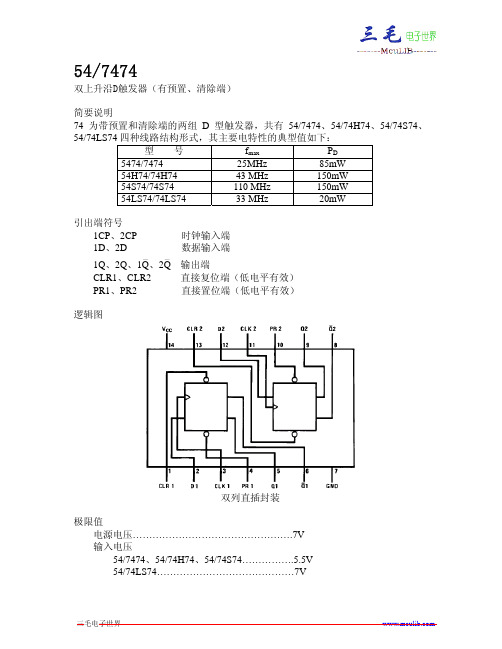
双上升沿D触发器(有预置、清除端)
简要说明
74 为带预置和清除端的两组 D 型触发器,共有 54/7474、54/74H74、54/74S74、
54/74LS74 四种线路结构形式,其主要电特性的典型
5474/7474
25MHz
85mW
54H74/74H74
43 MHz
VI=5.5V(‘LS74 为 PR,CLR
1
1
1
0.2
7V)
IIH 输 入 高 电 平 电 流
Vcc=最大
VIH=2.4V(‘S74 和’LS74 为 2.7V)
D CLR PR CP
40
50
50
120
150
150
80
100
100
80
100
100
20
40 40
uA
20
IIL输入低电平电 流
Vcc=最大 VIL=0.4V(‘S74 为
三毛电子世界
13.5
40
tPLH CP-Q
tPHL
_
CP-Q
25
15
9
25 ns
40
20
9
40
[2]:fmax-最大时钟频率,tPLH输出由低到高传输延迟时间,tPHL输出由高到低传输延迟时间
[3]:测tPHL(PR-Q_ ,CLR-Q),CP(H)时tPHL最大值为 13.5ns,CP(L)时tPHL最大值为 8ns
三毛电子世界
工作环境温度 54XXX …………………………………. -55~125℃ 74XXX …………………………………. 0~70℃
存储温度 ………………………………………….-65~150℃
SN74LVC157ADB中文资料

元器件交易网IMPORTANT NOTICETexas Instruments and its subsidiaries (TI) reserve the right to make changes to their products or to discontinueany product or service without notice, and advise customers to obtain the latest version of relevant informationto verify, before placing orders, that information being relied on is current and complete. All products are soldsubject to the terms and conditions of sale supplied at the time of order acknowledgement, including thosepertaining to warranty, patent infringement, and limitation of liability.TI warrants performance of its semiconductor products to the specifications applicable at the time of sale inaccordance with TI’s standard warranty. Testing and other quality control techniques are utilized to the extentTI deems necessary to support this warranty. Specific testing of all parameters of each device is not necessarilyperformed, except those mandated by government requirements.CERTAIN APPLICATIONS USING SEMICONDUCTOR PRODUCTS MAY INVOLVE POTENTIAL RISKS OFDEATH, PERSONAL INJURY, OR SEVERE PROPERTY OR ENVIRONMENTAL DAMAGE (“CRITICALAPPLICATIONS”). TI SEMICONDUCTOR PRODUCTS ARE NOT DESIGNED, AUTHORIZED, ORWARRANTED TO BE SUITABLE FOR USE IN LIFE-SUPPORT DEVICES OR SYSTEMS OR OTHERCRITICAL APPLICATIONS. INCLUSION OF TI PRODUCTS IN SUCH APPLICATIONS IS UNDERSTOOD TOBE FULLY AT THE CUSTOMER’S RISK.In order to minimize risks associated with the customer’s applications, adequate design and operatingsafeguards must be provided by the customer to minimize inherent or procedural hazards.TI assumes no liability for applications assistance or customer product design. TI does not warrant or representthat any license, either express or implied, is granted under any patent right, copyright, mask work right, or otherintellectual property right of TI covering or relating to any combination, machine, or process in which suchsemiconductor products or services might be or are used. TI’s publication of information regarding any thirdparty’s products or services does not constitute TI’s approval, warranty or endorsement thereof.Copyright © 1998, Texas Instruments Incorporated。
74HC02中文资料_数据手册_参数
INPUT nA, nB
UNIT LOADCOEFFICIENT 1.50
AC CHARACTERISTICS FOR 74HCT GND = 0 V; tr = tf = 6 ns; CL = 50 pF
SYMBOL PARAMETER
tPHL/ tPLH tTHL/ tTLH
min.
propagation delay nA, nB to nY
output transition time
Tamb (°C)
74HCT
+25
−40 to+85
typ. max. min. max.
11 19
24
7 15
19
−40 to+125 min. max.
29 22
UNIT
ns ns
TEST CONDITIONS
VCC WAVEFORMS (V)
4.5 Fig.6 4.5 Fig.6
For the DC characteristics see “74HC/HCT/HCU/HCMOS Logic Family Specifications”.
Output capability: standard ICC category: SSI
AC CHARACTERISTICS FOR 74HC GND = 0 V; tr = tf = 6 ns; CL = 50 pF
Quad 2-input NOR gate
Product specification
74HC/HCT02
DC CHARACTERISTICS FOR 74HCT For the DC characteristics see “74HC/HCT/HCU/HCMOS Logic Family Specifications”. Output capability: standard ICC category: SSI
74HC系列芯片资料

74HC00 四 2 输入与非门国际通用符号54/7400 , 54/74H00 , 54L 00 , 54/74S00 , 54/74LS00 , 54/74ALS00 , 54/ 74F 00 , 54/74HC00 , 54/ 74AC 00 , 54/74HCT00 , 54/74ACT00 , 54/74AHC00 , 54/74AHCT00 ,74LV00 , 74LVC00。
74HC02 四 2 输入或非门国际通用符号54/7402 , 54L 02 , 54/74S02 , 54/74LS02 , 54/74AS02 , 54/74ALS02 , 54/ 74F 02 ,54/74HC02 , 74AC 02 , 54/74HCT02 , 54/74ACT02 , 54/74AHC02 , 54/AHCT02 , 74LV02 , 74LVC02。
74HC04 六反相器国际通用符号54/7404 , 54L 04 , 54/74H04 , 54/74S04 , 54/74LS04 , 54/74AS04 , 54/74ALS04 ,54/ 74F 04 , 54/74HCU04 , 54/74HC04 , 54/ 74AC 04 , 54/74HCT04 , 54/74ACT04 ,54/74AHC04 , 54/74AHCT04 , 74LV04 , 74LVC04 , 54/74AHCU04 , 74LVU04 , 74LVCU04 .74HC08 四 2 输入与门国际通用符号54/7408 , 54/74S08 , 54/74LS08 , 54/74AS08 , 54/74ALS08 , 54/ 74F 08 , 54/74HC08 ,54/74HCT08 , 54/ 74AC 08 , 54/74ACT08 , 54/74AHC08 , 54/74AHCT08 , 74LV08 , 74LVC08。
- 1、下载文档前请自行甄别文档内容的完整性,平台不提供额外的编辑、内容补充、找答案等附加服务。
- 2、"仅部分预览"的文档,不可在线预览部分如存在完整性等问题,可反馈申请退款(可完整预览的文档不适用该条件!)。
- 3、如文档侵犯您的权益,请联系客服反馈,我们会尽快为您处理(人工客服工作时间:9:00-18:30)。
© Semiconductor Components Industries, LLC, 2012July, 2012 − Rev. 111Publication Order Number:
MC74HC157A/D
MC74HC157AQuad 2-Input DataSelectors / Multiplexers
High−Performance Silicon−Gate CMOSThe MC74HC157A is identical in pinout to the LS157. The deviceinputs are compatible with standard CMOS outputs; with pullupresistors, they are compatible with LSTTL outputs.This device routes 2 nibbles (A or B) to a single port (Y) asdetermined by the Select input. The data is presented at the outputs innoninverted form. A high level on the Output Enable input sets all fourY outputs to a low level.
Features•Output Drive Capability: 10 LSTTL Loads
•Outputs Directly Interface to CMOS, NMOS, and TTL
•Operating Voltage Range: 2.0 to 6.0 V
•Low Input Current: 1.0 mA
•High Noise Immunity Characteristic of CMOS Devices
•In Compliance with the Requirements Defined by JEDEC Standard
No. 7A•Chip Complexity: 82 FETs or 20.5 Equivalent Gates
•NLV Prefix for Automotive and Other Applications Requiring
Unique Site and Control Change Requirements; AEC−Q100Qualified and PPAP Capable•These Devices are Pb−Free, Halogen Free/BFR Free and are RoHS
Compliant
http://onsemi.com
See detailed ordering and shipping information in the packagedimensions section on page 2 of this data sheet.
ORDERING INFORMATION
MARKINGDIAGRAMS
SOIC−16D SUFFIXCASE 751B
TSSOP−16DT SUFFIXCASE 948F
116PDIP−16N SUFFIXCASE 648
116
116
1
16MC74HC157ANAWLYYWWG
116HC157AGAWLYWW
HC157AALYWGG
1
16
A=Assembly LocationL, WL=Wafer LotY, YY=YearW, WW=Work WeekG or G= Pb−Free Package
(Note: Microdot may be in either location)
芯天下--http://oneic.com/MC74HC157A
http://onsemi.com2
251114
361013
47912
115
A0A1A2A3
B0B1B2B3
Y0Y1Y2Y3
SELECTOUTPUTENABLE
DATAOUTPUTS
NIBBLEA INPUTS
NIBBLEB INPUTSPIN 16 = VCC
PIN 8 = GND
FUNCTION TABLEInputsOutputOutputsEnableSelectY0 − Y3
X = don’t careA0 − A3, B0 − B3 = the levels of therespective Data−Word Inputs.
HLLXLHLA0−A3B0−B3
Figure 1. Pin Assignment13141516910111254321876SELECTY0B0A0Y1B1A1GNDY3B3A3OUTPUTENABLE
VCC
B2A2Y2
Figure 2. Logic Diagram
ORDERING INFORMATIONDevicePackageShipping†MC74HC157ANGPDIP−16(Pb−Free)500 Units / Rail
MC74HC157ADGSOIC−16(Pb−Free)48 Units / RailMC74HC157ADR2GSOIC−16(Pb−Free)2500 / Tape & ReelMC74HC157ADTR2GTSSOP−16(Pb−Free)2500 / Tape & ReelNLV74HC157ADR2G*SOIC−16(Pb−Free)2500 / Tape & ReelNLV74HC157ADTR2G*TSSOP−16(Pb−Free)2500 / Tape & Reel†For information on tape and reel specifications, including part orientation and tape sizes, please refer to our Tape and Reel PackagingSpecifications Brochure, BRD8011/D.*NLV Prefix for Automotive and Other Applications Requiring Unique Site and Control Change Requirements; AEC−Q100 Qualified and PPAPCapable
芯天下--http://oneic.com/MC74HC157Ahttp://onsemi.com3
MAXIMUM RATINGSSymbolParameterValueUnitVCCDC Supply Voltage (Referenced to GND)– 0.5 to + 7.0VVinDC Input Voltage (Referenced to GND)– 0.5 to VCC + 0.5VVoutDC Output Voltage (Referenced to GND)– 0.5 to VCC + 0.5VIinDC Input Current, per Pin±20mAIoutDC Output Current, per Pin±25mAICCDC Supply Current, VCC and GND Pins±50mAPDPower Dissipation in Still Air,Plastic DIP†SOIC Package†TSSOP Package†750500450mW
TstgStorage Temperature– 65 to + 150_C
TLLead Temperature, 1 mm from Case for 10 Seconds(Plastic DIP, SOIC or TSSOP Package)260_C
Stresses exceeding Maximum Ratings may damage the device. Maximum Ratings are stressratings only. Functional operation above the Recommended Operating Conditions is not implied.Extended exposure to stresses above the Recommended Operating Conditions may affect devicereliability.†Derating—Plastic DIP: – 10 mW/_C from 65_ to 125_CSOIC Package: – 7 mW/_C from 65_ to 125_CTSSOP Package: − 6.1 mW/_C from 65_ to 125_C
RECOMMENDED OPERATING CONDITIONSSymbolParameterMinMaxUnitVCCDC Supply Voltage (Referenced to GND)2.06.0VVin, VoutDC Input Voltage, Output Voltage(Referenced to GND)0VCCV
TAOperating Temperature, All Package Types– 55+ 125_C
tr, tfInput Rise and Fall TimeVCC = 2.0 V(Figure 1)VCC = 4.5 VVCC = 6.0 V0001000500400ns
DC ELECTRICAL CHARACTERISTICS (Voltages Referenced to GND)
Guaranteed Limit
SymbolParameterTest ConditionsVCCV– 55 to25_Cv 85_Cv 125_CUnitVIHMinimum High−Level InputVoltageVout = VCC – 0.1 V|Iout| v 20 mA2.03.04.56.01.52.13.154.21.52.13.154.21.52.13.154.2V
VILMaximum Low−Level InputVoltageVout = 0.1 V|Iout| v 20 mA2.03.04.56.00.50.91.351.80.50.91.351.80.50.91.351.8VVOHMinimum High−Level OutputVoltageVin = VIH|Iout| v 20 mA2.04.56.01.94.45.91.94.45.91.94.45.9VVin = VIH|Iout| v 2.4 mA|Iout| v 6.0 mA|Iout| v 7.8 mA3.04.56.02.483.985.482.343.845.342.23.75.2