2305DATASHEET
鼎日DTS2305规格书
FEATURES
• Halogen-free Option Available • TrenchFET® Power MOSFET
APPLICATIONS
• Load Switch for Portable Devices
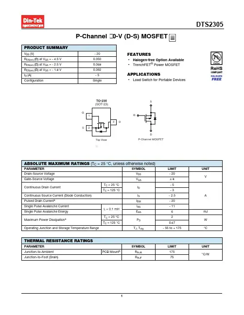
TO-236 (SOT-23)
G 1 3 S 2 D G
S
D Top View P-Channel MOSFET
2
DTS2305
TYPICAL CHARACTERISTICS (TA = 25 °C, unless otherwise noted)
20
VGS = 5 V thru 2 V
15
10
ID - Drain Current (A) ID - Drain Current (A)
12
TC = 25 °C
0.15 1200
Transfer Characteristics
0.12
RDS(on) - On-Resistance (Ω) C - Capacitance (pF)
1000
800
Ciss
0.09
VGS = 1.8 V
600
0.06
VGS = 2.5 V
400
Crss
Coss
0.03
VGS = 4.5 V
ABSOLUTE MAXIMUM RATINGS (TC = 25 °C, unless otherwise noted)
PARAMETER Drain-Source Voltage Gate-Source Voltage Continuous Drain Current Continuous Source Current (Diode Conduction) Pulsed Drain Currenta L = 0.1 mH TC = 25 °C TC = 125 °C Single Pulse Avalanche Current Single Pulse Avalanche Energy Maximum Power Dissipationa Operating Junction and Storage Temperature Range TC = 25 °C TC = 125 °C SYMBOL VDS VGS ID IS IDM IAS EAS PD TJ, Tstg LIMIT - 20 ±8 -5 -3 - 2.5 - 20 - 11 6 2 0.67 - 55 to + 175 mJ W °C A UNIT V
A3150光耦DataSheet

U E D P R O D U C T E F E R E N C E O N L Y .U250 f o r n e w d e s i g n Data Sheet 27621.40The A3150JLT and A3150JUA programmable switches provide tooth/valley recognition in large gear-tooth sensing applications. Each sensor consists of a single element, chopper-stabilized Hall-effect IC that can be programmed to the desired magnetic switch point, opti-mizing sensor airgap and timing accuracy performance after final packaging. The small package can be easily assembled and used in conjunction with a wide variety of gear/target shapes and sizes. The two devices differ only in package style.The sensing technology used for this sensor is Hall-effect based.The sensor incorporates a single-element Hall IC that switches inresponse to magnetic signals created by a ferrous target. The program-mability of the circuit eliminates magnet and system offsets such as those caused by tilt yet provides zero-speed detection capabilities without the associated running jitter inherent in classical digital solu-tions.A proprietary dynamic offset cancelation technique, with an internal high-frequency clock, reduces the residual offset voltage,which is normally caused by device overmolding, temperaturedependancies, and thermal stress. This technique produces devices that have an extremely stable quiescent output voltage, are immune to mechanical stress, and have precise recoverability after temperature cycling. Many problems normally associated with low-level analog signals are minimized by having the Hall element and amplifier in a single chip. Output precision is obtained by internal gain adjustments during the manufacturing process and operate-point programming in the user’s application.This sensor system is ideal for use in gathering speed, position, and timing information using gear-tooth-based configurations. TheA3150JLT/JUA are particularly suited to those applications that require accurate duty cycle control or accurate edge detection. The lower vibration sensitivity also makes these devices extremely useful for transmission speed sensing.3150Always order by complete part number: the prefix 'A' + the basic four-digit part number + a suffix to indicate operating temperature range +a suffix to indicate package style, e.g., A3150JLT .PROGRAMMABLE, CHOPPER-STABILIZED, HALL-EFFECT SWITCHContinued next page115 Northeast Cutoff, Box 15036Worcester, Massachusetts 01615-0036 (508) 853-********PROGRAMMABLE, CHOPPER-STABILIZED, PRECISION,HALL-EFFECT SWITCHCopyright © 2000, Allegro MicroSystems, Inc.Two package styles provide a magnetically opti-mized package for most applications. Suffix ‘–LT’ is a miniature SOT-89/TO-243AA transistor package for surface-mount applications; while suffix ‘–UA’ is a three-lead ultra-mini-SIP for through-hole mounting.FEATURES AND BENEFITSs Chopper Stabilized forExtremely Low Switch-Point Drift and Immunity to Mechanical Stresss Externally Programmed Switch Point s On-Chip Supply-Transient Protection s Output Short-Circuit Protections Single-Chip Sensing IC for High Reliability s Small Mechanical Size s <50µs Power-On Times Wide Operating Voltage Range s Defined Power-On State3150PROGRAMMABLE, CHOPPER-STABILIZED, PRECISION,HALL-EFFECT SWITCHLimitsCharacteristic Symbol Test ConditionsMin.Typ.Max.Units Operate PointB OPProgrammable offset range 500670850G Initial (before programming)02040G Resolution8.01114G ∆B OPV CC = 14 V, after programming, B OP ≈ 500 G-358.0+35G HysteresisB hys5.02035GNOTE: Typical data is at V CC = 5 V and T A = +25°C and is for design information only.ELECTRICAL CHARACTERISTICS over operating voltage and temperature range (unless otherwise noted).LimitsCharacteristic Symbol Test Conditions Min.Typ.Max.Units Supply Voltage V CC Operating, T J < 165°C4.25–26V Power-On State POS After programming, V CC = 0 ¡ 5 V HIGH HIGH HIGH –Low Output Voltage V OUT(SAT)I OUT = 20 mA –175400mV Output Current Limit I OUTM V OUT = 12 V 658095mA Output Leakage Current I OFF V OUT = 24 V–0.210µA Supply CurrentI CCBefore programming, output OFF – 4.07.0mA Before programming, output ON– 5.08.0mA Reverse Supply Current I RCC V RCC = -30 V ––-5.0mA Power-On Delay t on V CC > 5 V–2050µs Output Rise Time t r R L = 820 Ω, C L = 20 pF –200–ns Output Fall Time t f R L = 820 Ω, C L = 20 pF–100–ns Clock Frequency f C –340–kHz Zener Voltage V Z I ZT = 100 µA, T A = 25°C 2732–V Zener Impedancez zI ZT = 10 mA, T A = 25°C –50100ΩNOTE: Typical data is at V CC = 5 V and T A = +25°C and is for design information only.MAGNETIC CHARACTERISTICS over operating supply voltage and temperature ranges.115 Northeast Cutoff, Box 15036Worcester, Massachusetts 01615-0036 (508) 853-50003150PROGRAMMABLE, CHOPPER-STABILIZED, PRECISION,HALL-EFFECT SWITCHTYPICAL ELECTRICAL CHARACTERISTICS255075100AMBIENT TEMPERATURE IN °C-50Dwg. GH-053-2125-25S U P P L Y C U R R E N T I N m A5.04.03.02.01.015010152025SUPPLY VOLTAGE IN VOLTSDwg. GH-041-25S U P P L Y C U R R E N T I N m A10300AMBIENT TEMPERATURE IN °C200Dwg. GH-040-4S A T U R A T I O N V O L T A G E I N m V3150PROGRAMMABLE, CHOPPER-STABILIZED, PRECISION,HALL-EFFECT SWITCHFUNCTIONAL DESCRIPTIONChopper-Stabilized Technique. These devices use a proprietary dynamic offset cancellation technique, with an internal high-frequency clock to reduce the residual offset voltage of the Hall element that is normally caused by device overmolding, temperature dependencies, and thermal stress.This technique produces devices that have an extremely stable quiescent Hall output voltage, are immune to thermal stress, and have precise recoverability after temperature cycling. Thistechnique will also slightly degrade the device output repeatabil-ity.The Hall element can be considered as a resistor arraysimilar to a Wheatstone bridge. A large portion of the offset is a result of the mismatching of these resistors. The chopper-stabilizing technique cancels the mismatching of the resistors by changing the direction of the current flowing through the Hall plate and Hall voltage measurement taps, while maintaining the Hall-voltage signal that is induced by the external magnetic flux.The signal is, then, captured by a sample-and-hold circuit.Operation. The output of these devices switches low (turns ON) when a magnetic field (south pole) perpendicular to the Hall sensor exceeds the operate point threshold (B OP ). After turn-ON, the output is capable of sinking 25 mA and the output voltage is V OUT(SAT). When the magnetic field is reduced below the release point (B RP ), the device output goes high (turns OFF).The difference in the magnetic operate and release points is the hysteresis (B hys ) of the device. This built-in hysteresis allows clean switching of the output even in the presence of external mechanical vibration and electrical noise.Applications. It is strongly recommended that an external bypass capacitor be connected (in close proximity to the Hall sensor) between the supply and ground of the device to reduce both external noise and noise generated by the chopper-stabiliza-tion technique.The simplest form of magnet that will operate these devices is a bar magnet with the south-seeking pole towards the branded surface of the device. Many other methods of operation are possible. Extensive applications information on magnets and Hall-effect sensors is also available in the Allegro Electronic Data Book AMS-702 or Application Note 27701, orO U T P U T V O L T A G EFLUX DENSITYDwg. GH-007-2115 Northeast Cutoff, Box 15036Worcester, Massachusetts 01615-0036 (508) 853-50003150PROGRAMMABLE, CHOPPER-STABILIZED, PRECISION,HALL-EFFECT SWITCHPROGRAMMING PROTOCOLThe A3150JLT and A3150JUA operate points are pro-grammed by serially addressing the device through the supply terminal (pin1). After the correct operate point is determined, the device programming bits are selected and then a “lock” set to prevent any further (accidental)programming.Program Enable. To program the device, a sequence of pulses is used to activate/enable the addressing mode as shown in figure 1. This sequence of a V PP pulse, at least seven V PH pulses, and a V PP pulse with no supply interrup-tions, is designed to prevent the device from being pro-grammed accidentally (for example, as a result of noise on the supply line).VV V Dwg. WH-013Figure 1 — Program enablePROGRAMMING PROTOCOL over operating temperature range.LimitsCharacteristic Symbol DescriptionMin.Typ.Max.Units Programming VoltageV PL Minimum voltage during programming4.55.0 5.5V V PH 9.01011V V PP202325V Programming Current I PP Max. supply current during programming –250–mA Pulse Widtht d(0)OFF time between bits20––µs t d(1)Enable, address, program, or lock bit ON time 20––µs t dPProgram pulse ON time 100300–µs Pulse Rise Time t r V PL to V PH or V PP 11––µs Pulse Fall Timet fV PH or V PP to V PL 5.0––µsNOTE: Typical data is at T A = +25°C and is for design information only.3150PROGRAMMABLE, CHOPPER-STABILIZED, PRECISION,HALL-EFFECT SWITCH* In application, the terms “gear” and “target” are often interchanged. However, “gear” is preferred when motion is transferred.Address Determination. The operate point is adjust-able in 64 increments. With the appropriate target or gear*in position, the 64 switch points are sequentially selected (figure 2) until the required operate point is reached. Note that the difference between the operate point and the release point (hysteresis) is a constant for all addresses.Set-Point Programming. After the desired set-point address is determined (0 through 63), each bit of theequivalent binary address is programmed individually. For example, as illustrated in figure 3, to program address code 5 (binary 000101), bits 1 and 3 need to be programmed.Each bit is programmed during the wide V PP pulse and is not reversible.Lock Programming. After the desired set point is programmed, the program lock is then activated (figure 4)to prevent further programming of the device.V PV 0Dwg. WH-014A D D R E S S 0A D D R E S S 1A D D R E S S 2A D D R E S S N (UP T O 63)A D D R E S S N -1A D D R E S S N -2Figure 2 — Address determinationFigure 4 — Lock programmingV V VDwg. WH-016Figure 3 — Set-point programmingV V V Dwg. WH-015A115 Northeast Cutoff, Box 15036Worcester, Massachusetts 01615-0036 (508) 853-50003150PROGRAMMABLE, CHOPPER-STABILIZED, PRECISION,HALL-EFFECT SWITCHAll Allegro sensors are subjected to stringent qualification requirements prior to being released to production.To become qualified, except for the destructive ESD tests, no failures are permitted.CRITERIA FOR DEVICE QUALIFICATIONQualification Test Test Method and Test Conditions Test Length SamplesComments Biased Humidity (HAST)T A = 130°C, RH = 85%50 hrs 77V CC = V OUT = 5 V High-Temperature JESD22-A108,408 hrs77V CC = 24 V,Operating Life (HTOL)T A = 150°C, T J = 165°C V OUT = 20 V Accelerated HTOLJESD22-A108,504 hrs 77V CC = 24 V,T A = 175°C, T J = 190°C V OUT = 20 VAutoclave, Unbiased JESD22-A102, Condition C,96 hrs 77T A = 121°C, 15 psig High-Temperature MIL-STD-883, Method 1008,1000 hrs 77(Bake) Storage Life T A = 170°CTemperature CycleMIL-STD-883, Method 1010,500 cycles 77-65°C to +150°C Latch-Up—Pre/Post 6Reading Electro-Thermally—Pre/Post 6Induced Gate Leakage Reading ESD,CDF-AEC-Q100-002Pre/Post x per Test to failure,Human Body Model Reading test All leads > TBDElectrical DistributionsPer Specification—303150PROGRAMMABLE, CHOPPER-STABILIZED, PRECISION,HALL-EFFECT SWITCHSENSOR LOCATIONS(±0.005” [0.13 mm] die placement)Package Designators “UA” and "UA-TL"Although sensor location is accurate to three sigma for a particular design, product improvements may result in small changes to sensor location.Dwg. MH-008-80.030"0.76 mm NOMDwg. MH-011-9APackage Designator “LT”115 Northeast Cutoff, Box 15036Worcester, Massachusetts 01615-0036 (508) 853-50003150PROGRAMMABLE, CHOPPER-STABILIZED, PRECISION,HALL-EFFECT SWITCH0.440.35PACKAGE DESIGNATOR 'LT'(SOT-89/TO-243AA)Dimensions in Inches (for reference only)Dimensions in Millimeters (controlling dimensions)Dwg. MA-012-3 mmPads 1, 2, 3, and B — Low-Stress VersionPads 1, 2, and 3 only — Lowest Stress, But Not Self AligningNOTE: Exact body and lead configuration at vendor’s option within limits shown.Dwg. MA-012-3 inads 1, 2, 3, and B — Low-Stress Versionads 1, 2, and 3 only — Lowest Stress, But Not Self Aligning3150 PROGRAMMABLE, CHOPPER-STABILIZED, PRECISION,HALL-EFFECT SWITCH Surface-Mount Lead Form (Suffix '-TL')Dimensions in Inches (controlling dimensions)Dimensions in Millimeters (for reference only)PACKAGE DESIGNATOR 'UA'Dwg. MH-014E mm1.27BSC°Dwg. MH-014E inBSC°NOTES: 1.Tolerances on package height and width represent allowable mold offsets. Dimensions given are measured at the widest point (parting line).2.Exact body and lead configuration at vendor’s option within limits shown.3.Height does not include mold gate flash.4.Recommended minimum PWB hole diameter to clear transition area is 0.035” (0.89 mm).5.Where no tolerance is specified, dimension is nominal.115 Northeast Cutoff, Box 15036Worcester, Massachusetts 01615-0036 (508) 853-50003150PROGRAMMABLE, CHOPPER-STABILIZED, PRECISION,HALL-EFFECT SWITCHThe products described herein are manufactured under one or more of the following U.S. patents: 5,045,920; 5,264,783; 5,442,283;5,389,889; 5,581,179; 5,517,112; 5,619,137; 5,621,319; 5,650,719;5,686,894; 5,694,038; 5,729,130; 5,917,320; and other patents pending.Allegro MicroSystems, Inc. reserves the right to make, from time to time, such departures from the detail specifications as may be required to permit improvements in the performance, reliability, ormanufacturability of its products. Before placing an order, the user is cautioned to verify that the information being relied upon is current.Allegro products are not authorized for use as critical components in life-support appliances, devices, or systems without express written approval.The information included herein is believed to be accurate andreliable. However, Allegro MicroSystems, Inc. assumes no responsibil-ity for its use; nor for any infringements of patents or other rights of third parties that may result from its use.。
2305;中文规格书,Datasheet资料
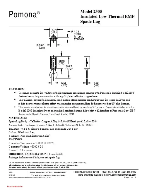
Pomona®All dimensions are in inches. Tolerances (except noted): .xx = ±.02” (,51 mm), .xxx = ± .005” (,127 mm).All specifications are to the latest revisions. Specifications are subject to change without notice.Registered trademarks are the property of their respective companies. Made in USA6/9/99Pomona ACCESS 90138 (800) 444-6785 or (425) 446-6010 SY/EH/LS More drawings available at Page 1 of 1 Model 2305 Insulated Low Thermal EMF Spade LugSales: 800-490-2361 Fax: 888-403-3360 Technical Assistance: 800-241-2060 FEATURES:• To ensure accurate low voltage or high resistance precision measurements, Pomona’s durable Model 2305features heavy duty construction with a gold plated tellurium copper base.• The tellurium copper/gold material combination offers superior conductivity and low oxide build-up andminimizes the thermoelectric effect, thus ensuring accurate readings in the nano-volt or 109 ohmic range.• The spade lug attaches to shunt terminals, standard binding posts or ¼” screws. For meter attachment, theModel 2305 is designed with an insulated standard banana jack which will interface to Pomona’s Low EMF Retractable Sheath Banana Plug Cord Model 5291.MATERIALS:Spade Lug Body – Tellurium Copper, Alloy 145, Gold Plated per MIL-G-45204Banana Jack – Tellurium Copper, Alloy 145, Gold Plated per MIL-G-45204Insulation – ABS Molded to Banana Jack and Spade Lug BodyColors: Black and Red, Marking: “Pomona Electronics, Calif.”RATINGS:Operating Temperature: +50°C (+122°F)Operating Voltage – 5000 VDCCurrent: 15 AmperesORDERING INFORMATION: Model 2305Package includes one black, one red spade lug/分销商库存信息: POMONA2305。
FT245BL-REEL,FT245BL-REEL, 规格书,Datasheet 资料
VIRTUAL COM PORT (VCP) DRIVERS for Windows 98 and Windows 98 SE Windows 2000 / ME / Server 2003 / XP Windows XP 64 Bit Windows XP Embedded Windows CE 4.2 MAC OS-8 and OS-9 MAC OS-X Linux 2.40 and greater Windows 98 and Windows 98 SE Windows 2000 / ME / Server 2003 / XP Windows XP 64 Bit Windows XP Embedded Windows CE 4.2 Linux 2.4 and Greater Easy MCU / PLD / FPGA interface to USB Upgrading Legacy Peripheral Designs to USB USB Instrumentation USB Industrial Control USB Audio and Low Bandwidth Video data transfer PDA USB data transfer USB MP3 Player Interface USB FLASH Card Reader / Writers Set Top Box (S.T.B.) PC - USB interface USB Digital Camera Interface USB Hardware Modems USB Wireless Modems
D2XX (USB Direct Drivers + DLL S/W Interface)
APPLICATION AREAS
2305芯片

2305芯片
2305芯片是一种高性能低功耗的微控制器芯片,适用于各种
智能设备和嵌入式系统。
该芯片采用先进的制造工艺和设计技术,集成了处理器核心、存储器和各种外设接口,具有强大的计算和控制能力。
首先,2305芯片采用先进的制造工艺,例如7纳米和14纳米
制程,确保芯片的性能和功耗方面的平衡。
先进的制造工艺可以在有限的面积上集成更多的晶体管,从而提供更高的计算能力和更低的功耗。
其次,2305芯片的处理器核心采用了先进的架构和指令集,
如ARM Cortex-M系列。
这些处理器核心具有高度优化的指令集和高度并行的执行单元,可以执行复杂的算法和实时控制任务。
同时,这些处理器核心还支持多核操作,可以平衡多个任务的执行。
第三,2305芯片具有丰富的外设接口,如串口、并行接口、
SD卡接口等。
这些外设接口可以与外部设备进行高速数据传
输和控制,实现与外部设备的连接和通信。
此外,2305芯片
还具有各种模拟接口,如模数转换器和比较器,可以实现对模拟信号的采集和处理。
第四,2305芯片还配备了大容量的存储器,包括闪存和RAM。
这些存储器可以存储程序代码、数据和配置信息,支持灵活的存储器管理和数据访问。
最后,2305芯片还支持多种通信协议,如CAN总线、SPI、I2C等。
通过这些通信协议,2305芯片可以与其他设备进行高效的数据交换和通信,实现设备之间的互连和协作。
总的来说,2305芯片是一款高性能低功耗的微控制器芯片,具有处理器核心、存储器和丰富的外设接口。
它适用于各种智能设备和嵌入式系统,提供强大的计算和控制能力,支持多核操作和多种通信协议。
LMX2305TMX;中文规格书,Datasheet资料
LMX2305LMX2305 PLLatinum Frequency Synthesizer for RF Personal CommunicationsLiterature Number: SNAS108ATL W 12459LMX2305 PLLatinum 550 MHz Frequency Synthesizer for RF Personal CommunicationsPRELIMINARYAugust1996 LMX2305PLLatinum TM550MHz Frequency Synthesizerfor RF Personal CommunicationsGeneral DescriptionThe LMX2305is a high performance frequency synthesizerwith an integrated prescaler designed for RF operation up to550MHz It is fabricated using National’s ABiC IV BiCMOSprocessThe LMX2305contains a dual modulus prescaler which canselect either a64 65or a128 129divide ratio at input fre-quencies of up to550MHz LMX2305 which employs thedigital phase lock loop technique combined with a highquality reference oscillator and a loop filter provides thetuning voltage for the voltage controlled oscillator to gener-ate a very stable low noise local oscillator signalSerial data is transferred into the LMX2305via a three lineMICROWIRE TM interface(Data Enable Clock) Supply volt-age can range from2 65V to5 5V The LMX2305featuresvery low current consumption typically4 0mA at2 75VThe LMX2305is available in a TSSOP20-pin surface mountplastic packageFeaturesY RF operation up to550MHzY2 65V to5 5V operationY Low current consumptionI CC e4 0mA(typ)at V CC e2 75VY Dual modulus prescaler 64 65or128 129Y Internal balanced low leakage charge pumpY Small-outline plastic surface mount TSSOP0 173 wide packageApplicationsY Analog Cellular telephone systems(AMPS ETACS NMT)Y Portable wireless communications(PCS PCN cordless)Y Wireless local area networks(WLANs)Y Other wireless communication systemsY PagersBlock DiagramTL W 12459–1TRI-STATE is a registered trademark of National Semiconductor CorporationMICROWIRE TM and PLLatinum TM are trademarks of National Semiconductor CorporationC1996National Semiconductor Corporation RRD-B30M126 Printed in U S A http www national com ObsoleteConnection DiagramLMX2305TL W 12459–220-Lead (0 173 Wide)Thin ShrinkSmall Outline Package (TM)Order Number LMX2305TM or LMX2305TMXSee NS Package Number MTC20Pin DescriptionsPin No Pin Name I O Description1OSC INIOscillator input A CMOS inverting gate input intended for connection to a crystal resonator for operation as an oscillator The input has a V CC 2input threshold and can be driven from an external CMOS or TTL logic gate May also be from a reference oscillator 3OSC OUTO Oscillator output4V P Power supply for charge pump Must be t V CC5V CC Power supply voltage input Input may range from 2 65V to 5 5V Bypass capacitors should be placed as close as possible to this pin and be connected directly to the ground plane 6D o OInternal charge pump output For connection to a loop filter for driving the input of an external VCO 7GND Ground8LD O Lock detect Output provided to indicate when the VCO frequency is in ‘‘lock’’ When the loop is locked the pin’s output is HIGH with narrow low pulses10f IN IPrescaler input Small signal input from the VCO 11CLOCK I High impedance CMOS Clock input Data is clocked in on the rising edge into the various counters and registers13DATA I Binary serial data input Data entered MSB first LSB is control bit High impedance CMOS input 14LEI Load enable input (with internal pull-up resistor) When LE transitions HIGH data stored in the shift registers is loaded into the appropriate latch (control bit dependent) Clock must be low when LE toggles high or low See Serial Data Input Timing Diagram15FC I Phase control select (with internal pull-up resistor) When FC is LOW the polarity of the phase comparator and charge pump combination is reversed16BISW OAnalog switch output When LE is HIGH the analog switch is ON routing the internal charge pump output through BISW (as well as through D o ) 17f OUT O Monitor pin of phase comparator input CMOS output18w pO Output for external charge pump w p is an open drain N-channel transistor and requires a pull-up resistor19PWDN IPower Down (with internal pull-up resistor) PWDN e HIGH for normal operation PWDN e LOW for power savingPower down function is gated by the return of the charge pump to a TRI-STATE condition 20w r OOutput for external charge pump w r is a CMOS logic output2 9 12NCNo connecthttp www national com2Ob s ol et eFunctional Block DiagramTL W 12459–3Note 1 The power down function is gated by the charge pump to prevent any unwanted frequency jumps Once the power down pin is brought low the part will go into power down mode when the charge pump reaches a TRI-STATE conditionhttp www national com3Ob s ol et eAbsolute Maximum Ratings (Notes 1and 2)If Military Aerospace specified devices are required please contact the National Semiconductor Sales Office Distributors for availability and specifications Power Supply Voltage V CC b 0 3V to a 6 5V V P b 0 3V to a 6 5V Voltage on Any Pin with GND e 0V (V I )b 0 3V to V CC a 0 3V Storage Temperature Range (T S )b 65 C to a 150 CLead Temperature (T L )(solder 4sec )a 260 CRecommended Operating ConditionsPower Supply Voltage V CC 2 65V to 5 5V V P V CC to a 5 5V Operating Temperature (T A )b 40 C to a 85 CNote 1 Absolute Maximum Ratings indicate limits beyond which damage to the device may occur Operating Ratings indicate conditions for which the device is intended to be functional but do not guarantee specific perform-ance limits For guaranteed specifications and test conditions see the Elec-trical Characteristics The guaranteed specifications apply only for the test conditions listedNote 2 This device is a high performance RF integrated circuit with an ESD rating k 2keV and is ESD sensitive Handling and assembly of this device should only be done at ESD workstationsElectrical Characteristics V CC e 2 75V V P e 2 75V b 40 C k T A k 85 C except as specifiedSymbol ParameterConditionsMinTyp Max Units I CC Power Supply Current 46mA I CC-PWDN Power Down Current30180m A f IN RF Input Operating Frequency 45550MHzf OSC Oscillator Input Operating Frequency 522MHz f w Phase Detector Frequency 10MHz Pf IN Input Sensitivity V CC e 2 65V to 5 5V b 10a 6dBmV OSC Oscillator Sensitivity OSC IN 0 5V PP V IH High-Level Input Voltage 0 7V CCV V IL Low-Level Input Voltage0 3V CCV I IH High-Level Input Current (Clock Data)V IH e V CC e 5 5Vb 1 01 0m A I IL Low-Level Input Current (Clock Data)V IL e 0V V CC e 5 5V b 1 01 0m A I IH Oscillator Input CurrentV IH e V CC e 5 5V 100m A I IL V IL e 0V V CC e 5 5V b 100m AI IH High-Level Input Current (LE FC)V IH e V CC e 5 5V b 1 01 0m A I ILLow-Level Input Current (LE FC)V IL e 0V V CC e 5 5Vb 1001 0m AExcept f IN and OSC INhttp www national com4Ob s ol et eElectrical Characteristics V CC e 2 75V V P e 2 75V b 40 C k T A k 85 C except as specified (Continued)Symbol ParameterConditionsMin TypMaxUnits I D o -source Charge Pump Output CurrentV D o e V P 2b 2 5b 1 0mA I D o -sink V D o e V P 21 02 5mAI D o -Tri Charge Pump TRI-STATE Current 0 5V s V D o s V P b 0 5V b 5 05 0nA T A e b 40 C k T A k 85 C V OH High-Level Output Voltage I OH e b 1 0mA V CC b 0 8VV OL Low-Level Output VoltageI OL e 1 0mA 0 4V V OH High-Level Output Voltage (OSC OUT )I OH e b 200m A V CC b 0 8V V OL Low-Level Output Voltage (OSC OUT )I OL e 200m A 0 4V I OL Open Drain Output Current (w p )V OL e 0 4V 1 0mA I OH Open Drain Output Current (w p )V OH e 2 75V 100m A t CS Data to Clock Set Up Time See Data Input Timing 50ns t CH Data to Clock Hold Time See Data Input Timing 10ns t CWH Clock Pulse Width High See Data Input Timing 50ns t CWL Clock Pulse Width Low See Data Input Timing 50ns t ES Clock to Enable Set Up Time See Data Input Timing 50ns t EWEnable Pulse WidthSee Data Input Timing50nsExcept OSC OUThttp www national com5Ob s ol et eFunctional DescriptionThe simplified block diagram below shows the 19-bit data register the 14-bit R Counter and the R15Latch and the 18-bit N Counter (intermediate latches are not shown) The data stream is clocked (on the rising edge)into the DATA input MSB first If the Control Bit (last bit input)is HIGH the DATA is transferred into the R Counter (programmable reference divider)and the S Latch (prescaler select 64 65or 128 129) If the Control Bit (LSB)is LOW the DATA is transferred into the N Counter (programmable divider)TL W 12459–1PROGRAMMABLE REFERENCE DIVIDER (R COUNTER)AND PRESCALER SELECT (R15LATCH)If the Control Bit (last bit shifted into the Data Register)is HIGH data is transferred from the 19-bit shift register into a 14-bit latch (which sets the 14-bit R Counter)and the 1-bit R15Latch which sets the prescaler 64 65or 128 129 Serial data format is shown belowTL W 12459–1414-BIT PROGRAMMABLE REFERENCE DIVIDER RATIO (R COUNTER)Divide14R 13R 12R 11R 10R R 9R 8R 7R 6R 5R 4R 3R 2R1RatioR 3000000000000114000000100###############1638311111111111111Notes Divide ratios less than 3are prohibitedDivide ratio 3to 16383R1to R14 These bits select the divide ratio of the programmable reference dividerC Control bit (set to HIGH level to load R counter and R15Latch)Data is shifted in MSB first1-BIT PRESCALER SELECT (R15LATCH)Prescaler 15R Select P 128 129064 651http www national com6Ob s ol et eFunctional Description (Continued)PROGRAMMABLE DIVIDER (N COUNTER)The N counter consists of the 7-bit swallow counter (A counter)and the 11-bit programmable counter (B counter) If the Control Bit (last bit shifted into the Data Register)is LOW data is transferred from the 19-bit shift register into a 7-bit latch which sets the 7-bit Swallow (A)Counter and an 11-bit latch which sets the 11-bit programmable (B)Counter Serial data format is shown belowTL W 12459–15Note S8to S18 Programmable counter divide ratio control bits (3to 2047)7-BIT SWALLOW COUNTER DIVIDE RATIO (A COUNTER)Divide N 7N 6N 5N 4N 3N 2N 1Ratio A 0000000011########1271111111Note Divide ratio 0to 127B t A11-BIT PROGRAMMABLE COUNTER DIVIDE RATIO (B COUNTER)Divide 18N 17N 16N 15N 14N 13N 12N 11N 10N N 9N 8Ratio B 30000000001141############204711111111111Note Divide ratio 3to 2047(Divide ratios less than 3are prohibited)B t APULSE SWALLOW FUNCTION f VCO e (P c B)a A c f OSC Rf VCO Output frequency of external voltage controlled oscil-lator (VCO)B Preset divide ratio of binary 11-bit programmablecounter (3to 2047)APreset divide ratio of binary 7-bit swallow counter (0s A s 127 A s B)f OSC Output frequency of the external reference frequencyoscillator R Preset divide ratio of binary 14-bit programmable ref-erence counter (3to 16383)P Preset modulus of dual modulus prescaler (64or 128)http www national com7Ob s ol et eFunctional Description (Continued)SERIAL DATA INPUT TIMINGTL W 12459–16Notes Parenthesis data indicates programmable reference divider dataData shifted into register on clock rising edge Data is shifted in MSB firstTest Conditions The Serial Data Input Timing is tested using a symmetrical waveform around V CC 2 The test waveform has an edge rate of 0 6V ns withamplitudes of 2 2V V CC e 2 7V and 2 6V V CC e 5 5VPhase CharacteristicsIn normal operation the FC pin is used to reverse the polari-ty of the phase detector Both the internal and any external charge pump are affectedDepending upon VCO characteristics FC pin should be set accordinglyWhen VCO characteristics are like (1) FC should be set HIGH or OPEN CIRCUITWhen VCO characteristics are like (2) FC should be set LOWWhen FC is set HIGH or OPEN CIRCUIT the monitor pin of the phase comparator input f out is set to the reference divider output f r When FC is set LOW f out is set to the programmable divider output f pVCO CharacteristicsTL W 12459–17PHASE COMPARATOR AND INTERNAL CHARGE PUMP CHARACTERISTICSTL W 12459–18Notes Phase difference detection range b 2q to a 2qThe minimum width pump up and pump down current pulses occur at the D o pin when the loop is locked FC e HIGHhttp www national com8Ob s ol et eAnalog SwitchThe analog switch is useful for radio systems that utilize a frequency scanning mode and a narrow band mode The purpose of the analog switch is to decrease the loop filter time constant allowing the VCO to adjust to its new frequency in a shorter amount of time This is achieved by adding another filter stage in parallel The output of the charge pump is normally through the D o pin but when LE is set HIGH the charge pump output also becomes available at BISW A typical circuit is shown below The second filter stage (LPF-2)is effective only when the switch is closed (in the scanning mode)TL W 12459–19Typical Crystal Oscillator CircuitA typical circuit which can be used to implement a crystal oscillator is shown belowTL W 12459–20Typical Lock Detect CircuitA lock detect circuit is needed in order to provide a steady LOW signal when the PLL is in the locked state A typical circuit is shown belowTL W 12459–21http www national com9Ob s ol e t e分销商库存信息: NATIONAL-SEMICONDUCTOR LMX2305TMX。
LED降压恒流驱动IC
LED降压恒流驱动IC大功率LED驱动IC-TAC7135 价格为:1.2元TAC Microtech(台创科技)针对大功率LED(发光二极管)的不同应用推出一款解决方案TAC7135。
TAC7135是一款输入电压2.7V-6V 的350mA超低压差稳流器。
350mA恒定电流输出推动1W的大功率LED,达到稳定亮度、增加电池总输出功率的效果,输出电流分别有300mA、330mA、350mA、380mA,其超低压差、低静态电流特性更延长了电池使用时间。
使用两个380mA并联则可直接驱动3W大功率LED,无须任何外接组件,并具有输出短路/开路保护与内建过热保护装置。
SOT-89-3封装。
应用范围:大功率LED手电筒、大功率LED矿灯、低压降压模块、汽车LED灯、LED灯箱、LED台灯照明, 并可直接代替AMC7135。
规格书下载:TAC7135大功率LED驱动IC-TAC7136 价格为:1.5元TAC7136 是一款低静态电流、低压差的LED恒流驱动器。
输入电压2.7V-6V,使用一个外接电阻,可使输出电流能在100mA到400mA范围内进行调节。
仅仅需要一个外接电阻就可构成一个完整的LED恒流驱动电路。
内部自带软启动、过热保护、低压保护。
提供一个可以用于扩压和扩流的DR脚。
外接一个MOS 场效应管或NPN三极管,可以扩大输出电流和输出电压范围,最大电流可达2A。
SOT-89-5封装。
应用范围:大功率LED手电筒、大功率LED矿灯、低压降压模块、汽车LED灯、LED灯箱、LED台灯照明,LED 显微镜灯。
规格书下载:TAC7136大功率LED驱动IC-TAC9920 价格为:1.5元TAC9920 是一款高效率,稳定可靠的大功率LED驱动IC,内置高精度比较器,off-time控制电路,恒流驱动控制电路等,特别适合大功率,多个大功率LED灯串恒流驱动。
TAC9920采用固定off-time控制方式,其工作频率可高达2.5MHz,可使外部电感和滤波电容,体积减少,效率提高。
OB2535_DataSheet
OB2535High Precision CC/CV Primary-Side PWM Power SwitchGENERAL DESCRIPTIONOB2535 is a high performance offline PWM Power switch for low power AC/DC charger and adaptor applications. It operates in primary-side sensing and regulation. Consequently, opto-coupler and TL431 could be eliminated. Proprietary Constant Voltage (CV) and Constant Current (CC) control is integrated as shown in the figure below.In CC control, the current and output power setting can be adjusted externally by the sense resistor Rs at CS pin. In CV control, multi-mode operations are utilized to achieve high performance and high efficiency. In addition, good load regulation is achieved by the built-in cable drop compensation. Device operates in PFM in CC mode as well at large load condition and it operates in PWM with frequency reduction at light/medium load.OB2535 offers power on soft start control and protection coverage with auto-recovery features including Cycle-by-Cycle current limiting, VDD OVP, VDD clamp and UVLO. Excellent EMI performance is achieved with On-Bright proprietary frequency shuffling technique.High precision constant voltage (CV) and constant current (CC) can be achieved by OB2535..Fig.1. Typical CC/CV CurveFEATURES5% Constant Voltage Regulation, 5% ConstantCurrent Regulation at Universal AC input Primary-side Sensing and Regulation WithoutTL431 and Opto-couplerProgrammable CV and CC RegulationAdjustable Constant Current and Output PowerSettingBuilt-in Secondary Constant Current Controlwith Primary Side FeedbackBuilt-in Adaptive Current Peak Regulation Built-in Primary winding inductancecompensationProgrammable Cable drop Compensation Power on Soft-startBuilt-in Leading Edge Blanking (LEB) Cycle-by-Cycle Current LimitingVDD Under Voltage Lockout with Hysteresis(UVLO) VDD OVP VDD ClampAPPLICATIONSLow Power AC/DC offline SMPS for Cell Phone ChargerDigital Cameras Charger Small Power AdaptorAuxiliary Power for PC, TV etc.Linear Regulator/RCC ReplacementOB2535 is offered in SOP8 package.TYPICAL APPLICATIONPreliminaryOB ri g nf i d e nt i al to创裕OB2535High Precision CC/CV Primary-Side PWM Power SwitchGENERAL INFORMATIONPin ConfigurationThe pin map is shown as below for SOP8VDD COMP INVCSGND GNDOrdering Information Part Number Description OB2535CP SOP8, Pb-free, Tube OB2535CPA SOP8, Pb-free, T&RPackage Dissipation Rating Package R θJA (℃/W) SOP8 90Note: Drain Pin Connected 100mm 2 PCB copper clad.Absolute Maximum RatingsParameter Value Drain Voltage (off state) -0.3V to Bvdss VDD Voltage -0.3 to V DD_clamp VDD Zener Clamp Continuous Current 10 mA COMP Voltage -0.3 to 7V CS Input Voltage -0.3 to 7V INVInput Voltage -0.3 to 7V Min/Max Operating Junction Temperature TJ-20 to 150 o C Min/Max Storage Temperature T stg -55 to 150 o C Lead Temperature (Soldering, 10secs) 260o CNote: Stresses beyond those listed under “absolute maximumratings” may cause permanent damage to the device. These are stress ratings only, functional operation of the device at these or any other conditions beyond those indicated under “recommended operating conditions” is not implied. Exposure to absolute maximum-rated conditions for extended periods may affect device reliability.PreliminaryOn -B rt Co nf i d e nt i al to创裕OB2535High Precision CC/CV Primary-Side PWM Power SwitchMarking InformationTERMINAL ASSIGNMENTSPin Num Pin Name I/O Description1 VDD P Power Supply2 COMP I Loop Compensation for CV Stability3 INV I The voltage feedback from auxiliary winding. Connected to resistor dividerfrom auxiliary winding reflecting output voltage. PWM duty cycle isdetermined by EA output and current sense signal at pin 4.4 CS I Current sense input5/6 DRAIN OHV MOSFET Drain Pin. The Drain pin is connected to the primary lead ofthe transformer7/8 GND P GroundOUTPUT POWER TABLE230VAC±15% 85-264VACProduct Adapter 1Adapter 1 OB2535 6W 5WNotes:1.Maximum practical continuous power in an Adapter design with sufficient drain pattern as a heat sink, at 50℃ ambient.PreliminaryOn -B ri g ht Co nf i de nt i al to创裕BLOCK DIAGRAMOn -B ri g ht CELECTRICAL CHARACTERISTICS(T A = 25O C, VDD=VDDG=16V, if not otherwise noted)Symbol Parameter Test Conditions Min Typ Max UnitSupply Voltage (VDD) Section I DD ST Standby Current VDD=13V5 20uA I DD op Operation CurrentOperation supply current INV=2V, CS=0V,VDD=VDDG=20V- 2.5 3.5 mAUVLO(ON) VDD Under Voltage Lockout Enter VDD falling 8.2 9.0 10.5 VUVLO(OFF) VDD Under Voltage Lockout Exit VDD rsing13.5 14.5 16.0V V DD _clamp Maximum VDD operationvoltageI DD =10mA29.5 31.5 33.5V OVPOver voltage protection ThresholdRamp VDD until gate shut down 27.5 29.5 31.5VCurrent Sense Input SectionTLEB LEB time540 ns Vth_oc Over current threshold870 900 930 mVTd_oc OCP Propagation delay150 ns Z SENSE _IN Input Impedance50 KohmT_ssSoft start time10msFrequency SectionFreq_Max Note 1 IC Maximum frequency 60 65 70 KHzFreq_NomSystem Nominal switch frequency60KHzFreq_startup INV =0V, Comp =5V 14 KHz △f/FreqFrequency shuffling range+/-4% Error Amplifier section Vref_EA Reference voltage for EA 1.97 2 2.03V GainDC gain of EA60 dB I_COMP_MAXMax. Cable compensationcurrentINV=2V, Comp=0V45uAPower MOSFET Section BVdss MOSFET Drain-Source Breakdown Voltage 600 V RdsonOn ResistanceStatic, Id=0.4A1215ΏNote:1. Freq_Max indicates IC internal maximum clock frequency. In system application, the maximum operation frequency of 60Khz nominal occurs at maximum output power or the transition point from CV to CC.On -B ri ght Co nf i de nt i al to创裕CHARACTERIZATION PLOTSOn -B ri g ht Co nf i dOPERATION DESCRIPTIONOB2535 is a cost effective PWM power switch optimized for off-line low power AC/DC applications including battery chargers and adaptors. It operates in primary side sensing and regulation, thus opto-coupler and TL431 are not required. Proprietary built-in CV and CC control can achieve high precision CC/CV control meeting most adaptor and charger application requirements.z Startup Current and Start up ControlStartup current of OB2535 is designed to be very low so that VDD could be charged up above UVLO threshold and starts up quickly. A large value startup resistor can therefore be used to minimize the power loss in application.z Operating CurrentThe Operating current of OB2535 is as low as 2.5mA. Good efficiency is achieved with the low operating current together with ‘Muti-mode’ control features.z Soft StartOB2535 features an internal soft start to minimize the component electrical over-stress during power on startup. As soon as VDD reaches UVLO (OFF), the control algorithm will ramp peak current voltage threshold gradually from nearly zero to normal setting of 0.90V. Every restart is a soft start.z CC/CV OperationOB2535 is designed to produce good CC/CV control characteristic as shown in the Fig. 1.In charger applications, a discharged battery charging starts in the CC portion of the curve until it is nearly full charged and smoothly switches to operate in CV portion of the curve.In an AC/DC adapter, the normal operation occurs only on the CV portion of the curve. The CC portion provides output current limiting. In CV operation, the output voltage is regulated through the primary side control. In CC operation mode, OB2535 will regulate the output current constant regardless of the output voltage drop.z Principle of OperationTo support OB2535 proprietary CC/CV control, system needs to be designed in DCM mode for flyback system (Refer to Typical Application Diagram on page1).In the DCM flyback converter, the output voltage can be sensed via the auxiliary winding. During MOSFET turn-on time, the load current is supplied from the output filter capacitor Co. The current inthe primary winding ramps up. When MOSFET turns off, the primary current transfers to the secondary at the amplitude ofP SPS I N N I ⋅=(1) The auxiliary voltage reflects the output voltage as shown in fig.2 and it is given by)(V V N N V O SAUXAUX Δ+⋅=(2) Where ΔV indicates the drop voltage of the output Diode.Fig.2. Auxiliary voltage waveformVia a resistor divider connected between the auxiliary winding and INV (pin 3), the auxiliary voltage is sampled at the end of the de-magnetization and it is hold until the next sampling. The sampled voltage is compared with Vref (2.0V) and the error is amplified. The error amplifier output COMP reflects the load condition and controls the PWM switching frequency to regulate the output voltage, thus constant output voltage can be achieved.When sampled voltage is below Vref and the error amplifier output COMP reaches its maximum, the switching frequency is controlled by the sampled voltage thus the output voltage to regulate the output current, thus the constant output current can be achieved.z Adjustable CC point and Output PowerIn OB2535, the CC point and maximumoutput power can be externally adjusted by external current sense resistor Rs at CS pin as illustrated in Typical Application Diagram. The output power is adjusted through CC point change. The larger Rs, the smaller CC point is, and the smaller output power becomes, and vice versa as shown in Fig.3.On -B ri g ht Co nf创裕Fig.3 Adjustable output power by changing Rsz Operation switching frequencyThe switching frequency of OB2535 is adaptively controlled according to the load conditions and the operation modes. No external frequency setting components are required. The operation switching frequency at maximum output power is set to 60K Hz internally.For flyback operating in DCM, The maximum output power is given by221p SW P MAX I F L Po =(3) Where Lp indicate the inductance of primary winding and Ip is the peak current of primary winding.Refer to the equation 3, the change of the primary winding inductance results in the change of the maximum output power and the constant output current in CC mode. To compensate the change from variations of primary winding inductance, the switching frequency is locked by an internal loop such that the switching frequency isDemagSW T F 21=(4)Since T Demag is inversely proportional to the inductance, as a result, the product Lp and fsw is constant, thus the maximum output power and constant current in CC mode will not change as primary winding inductance changes. Up to +/-10% variation of the primary winding inductance can be compensated.z Frequency shuffling for EMI improvement The frequency shuffling (switching frequency modulation) is implemented in OB2535. The oscillation frequency is modulated so that the tone energy is spread out. The spread spectrum minimizes the conduction band EMI and therefore eases the system design.z Gate DriveThe internal power MOSFET in OB2535 is driven by a dedicated gate driver for power switch control. Too weak the gate drive strength results in higher conduction and switch loss of MOSFET while too strong gate drive compromises EMI.A good tradeoff is achieved through the built-in totem pole gate design with right output strength control.z Programmable Cable drop CompensationIn OB2535, cable drop compensation is implemented to achieve good load regulation. An offset voltage is generated at INV by an internal current flowing into the resister divider. The current is inversely proportional to the voltage across pin COMP, as a result, it is inversely proportional to the output load current, thus the drop due to the cable loss can be compensated. As the load current decreases from full-load to no-load, the offset voltage at INV will increase. It can also be programmed by adjusting the resistance of the divider to compensate the drop for various cable lines used.z Protection ControlGood power supply system reliability is achieved with its rich protection features including Cycle-by-Cycle current limiting (OCP), VDD clamp, Power on Soft Start, and Under Voltage Lockout on VDD (UVLO).VDD is supplied by transformer auxiliary winding output. The output of OB2535 is shut down when VDD drops below UVLO (ON) limit and Switcher enters power on start-up sequence thereafter.On -B ri g ht Co nf i d e nt i al to创裕PACKAGE MECHANICAL DATADimensions In Millimeters Dimensions In InchesSymbolMin Max Min MaxA 1.350 1.750 0.053 0.069 A1 0.050 0.250 0.002 0.010 A2 1.250 1.650 0.049 0.065 b 0.310 0.510 0.012 0.020 c 0.170 0.250 0.006 0.010D 4.700 5.150 0.185 0.203E 3.800 4.000 0.150 0.157 E1 5.800 6.200 0.228 0.244 e 1.270 (BSC) 0.05 (BSC)L 0.400 1.270 0.016 0.050 θ 0º 8º 0º 8ºOn -B ri g ht Co nf i d e nt i al to创裕IMPORTANT NOTICERIGHT TO MAKE CHANGESOn-Bright Electronics Corp. reserves the right to make corrections, modifications, enhancements, improvements and other changes to its products and services at any time and to discontinue any product or service without notice. Customers should obtain the latest relevant information before placing orders and should verify that such information is current and complete.WARRANTY INFORMATIONOn-Bright Electronics Corp. warrants performance of its hardware products to the specifications applicable at the time of sale in accordance with its standard warranty. Testing and other quality control techniques are used to the extent it deems necessary to support this warranty. Except where mandated by government requirements, testing of all parameters of each product is not necessarily performed.On-Bright Electronics Corp. assumes no liability for application assistance or customer product design. Customers are responsible for their products and applications using On-Bright’s components, data sheet and application notes. To minimize the risks associated with customer products and applications, customers should provide adequate design and operating safeguards.LIFE SUPPORTOn-Bright Electronics Corp.’s products are not designed to be used as components in devices intended to support or sustain human life. On-bright Electronics Corp. will not be held liable for any damages or claims resulting from the use of its products in medical applications.MILITARYOn-Bright Electronics Corp.’s products are not designed for use in military applications. On-Bright Electronics Corp. will not be held liable for any damages or claims resulting from the use of its products in military applications.On -B ri g ht Co nf i d e nt i al to创裕。
AP2305N中文资料
Advanced Power P-CHANNEL ENHANCEMENT MODE Electronics Corp.POWER MOSFET▼Simple Drive Requirement BV DSS-20V▼Small Package Outline R DS(ON)65mΩ▼Surface Mount Device I D- 4.2ADescriptionAbsolute Maximum RatingsSymbol UnitsV DS VV GS VI D@T A=25℃AI D@T A=70℃AI DM AP D@T A=25℃WW/℃T STG℃T J℃Symbol Value Unit Rthj-amb Thermal Resistance Junction-ambient3Max.90℃/WData and specifications subject to change without notice-55 to 150Linear Derating FactorThermal DataParameterTotal Power DissipationOperating Junction Temperature RangeStorage Temperature Range1.38-55 to 150ParameterDrain-Source VoltageGate-Source VoltageContinuous Drain Current3Continuous Drain Current3-3.4Pulsed Drain Current1,2-102004280301AP2305NRating- 20± 12-4.20.01The Advanced Power MOSFETs from APEC provide thedesigner with the best combination of fast switching,, low on-resistance and cost-effectiveness.The SOT-23 package is universally preferred for all commercial-industrial surface mount applications and suited for low voltageapplications such as DC/DC converters.DGSSOT-23AP2305NElectrical Characteristics@T j=25o C(unless otherwise specified) Symbol Parameter Test Conditions Min.Typ.Max.UnitsBV DSS Drain-Source Breakdown Voltage V GS=0V, I D=-250uA-20--V ΔB V DSS/ΔT j Breakdown Voltage Temperature Coefficient Reference to 25℃, I D=-1mA--0.1-V/℃R DS(ON)Static Drain-Source On-Resistance V GS=-10V, I D=-4.5A--53mΩV GS=-4.5V, I D=-4.2A--65mΩV GS=-2.5V, I D=-2.0A--100mΩV GS=-1.8V, I D=-1.0A--250mΩV GS(th)Gate Threshold Voltage V DS=V GS, I D=-250uA-0.5--V g fs Forward Transconductance V DS=-5V, I D=-2.8A-9-S I DSS Drain-Source Leakage Current (Tj=25o C)V DS=-20V, V GS=0V---1uA Drain-Source Leakage Current (T j=55o C)V DS=-16V, V GS=0V---10uAI GSS Gate-Source Leakage VGS=--nA Q g Total Gate Charge2I D=-4.2A-10.6-nC Q gs Gate-Source Charge V DS=-16V- 2.32-nC Q gd Gate-Drain ("Miller") Charge V GS=-4.5V- 3.68-nC t d(on)Turn-on Delay Time2V DS=-15V- 5.9-ns t r Rise Time I D=-4.2A- 3.6-ns t d(off)Turn-off Delay Time R G=6Ω,V GS=-10V-32.4-ns t f Fall Time R D=3.6Ω- 2.6-ns C iss Input Capacitance V GS=0V-740-pF C oss Output Capacitance V DS=-15V-167-pF C rss Reverse Transfer Capacitance f=1.0MHz-126-pF Source-Drain DiodeSymbol Parameter Test Conditions Min.Typ.Max.Units V SD Forward On Voltage2I S=-1.2A, V GS=0V---1.2V trr Reverse Recovery Time I S=-4.2A, V GS=0V,-27.7-ns Qrr Reverse Recovery Charge dI/dt=100A/µs-22-nCNotes:1.Pulse width limited by Max. junction temperature.2.Pulse width <300us , duty cycle <2%.3.Surface mounted on 1 in2 copper pad of FR4 board ; 270℃/W when mounted on min. copper pad.± 12V±100AP2305NFig 3. On-Resistance v.s. Gate VoltageFig 4. Normalized On-Resistancev.s. Junction TemperatureFig 6. Gate Threshold Voltage v.s. Reverse DiodeJunction TemperatureAP2305NFig 7. Gate Charge Characteristics Fig 8. Typical Capacitance CharacteristicsFig 9. Maximum Safe Operating Area Fig 10. Effective Transient Thermal ImpedanceFig 11. Switching Time Circuit Fig 12. Gate Charge Circuit。
1230;1495;5070;5071;5072;中文规格书,Datasheet资料
1CAT.NO.1236.025SQUARE WIRE WRAP PINSCONTACT PINS (SEAMLESS)Completely burr free straight to within .003(.08)per inch.Conical ends of square-wire with smooth blend-in radius on corners assures ease of insertion with minimum damage to pre-plated PCB holes.Pins can be staked to .062(1.57)and .093(2.36)thick boards.“FLEA”CLIP“IMP”TERMINAL“MICRO”TERMINALFor subminiature applications where conventional terminals are too large or too costly.Ideal for quick repairs of printed circuitry.Simply insert wire through hole and it is held firmly by spring action assuring continued postive contact.•Quick and Easy to Install •For Production or Prototype•Postive Locking In-Hole •No Staking Required •Holds .010(.25)to .050(1.27)Diameter WireThese terminals are often used for transistor and Bi-Pin lamp sockets.Terminals snap into place and are firmly held without the need of staking.Wire leads can be inserted from either end.Terminals 1236and 1237have tapered socket spring forming that will hold multiple leads in place.Terminals are pre-tinned for easy soldering.CAT.NO.1237CAT.NO.1238Easily press-fit into a .042(1.07)diameter hole may be flared for permanent installation.Ideally designed for use in circuitry to support components when space is at a premium.CAT.NO.1495Excellent for point to point or feed thru wiring.Slot is serrated to grip component leads.Multiple connections are made quick and easy.CLAMP TERMINALCAT.NO.1499FTCAT.NO.1500Terminal for production or prototype use.Holds as many as 7leads without soldering,by spring action.CAT.NO.1498CPAAB.125 [3.2].034[.86].025[.64]60°L.010[.25].003R .[.08 R ].812[20.6].260[6.6].032[0.81].085[2.16].085[2.16].312[7.9].062[1.57].234 [6.0]REF..040[1.02]DIA..094[2.39]CAT.NO.A B 1223.093(2.36).293(7.4)1224.093(2.36).357(9.1)1226.093(2.36).437(11.1)1200.125(3.18).379(9.6)1210.125(3.18).566(14.4)1230.156(3.96).379(9.6)1231.156(3.96).566(14.4)MATERIAL:Phosphor Bronze,Tin PlateMATERIAL:Brass,Nickel Plate.375[9.6].187[4.8].053 [1.34].053[1.35]REF..058[1.48].052 [1.32].064 [1.7].078 [1.98]REF..030[.76].130 [3.3].045[1.14]DIA..237[6.0].437[11.1].063 [1.6] REF..046 [1.17].100 [2.6].078 [1.98].359[9.1].167[4.3].030 [.76].034 [.86].031 [.79]DIA..018 [.46]DIA..065 [1.65]DIA..080 [2.03]DIA. FLANGE.050 [1.27]I.DIA..219[5.6].328[8.4].047 [1.19].188[4.8].469[11.9].219[5.6].080 [2.03]DIA. FLANGE.050[1.27]I.DIA..065[1.65]DIA..065[1.65]DIA..080[2.03]DIA.FLANGE.050[1.27]I.DIA..219[5.6].046[1.17]DIA.FLARE.469[11.9].188[4.8]Insertion Tool:CAT.NO.1323Insertion Tool:CAT.NO.1322Insertion Tool:CAT.NO.1322Insertion Tool:CAT.NO.1322Mtg.Hole .062(1.57)Mtg.Hole .062(1.57)Mtg.Hole .093(2.36)MATERIAL:.006(.15)Matte Tin,Brass.Pre-TinnedMATERIAL:.008(.20)Matte Tin,Beryllium Copper,Tin PlateMATERIAL:.008(.20)Matte Tin,Beryllium Copper,Tin PlateMATERIAL:.015(.38)Matte Tin,Spring Steel,Tin PlateMATERIAL:.008(.20)Matte Tin,Beryllium Copper,Tin Plate MATERIAL:.006(.15)Matte Tin,Brass.Pre-TinnedMATERIAL:.006(.15)Matte Tin,Brass.Pre-Tinned.062(1.57)—.067(1.70)Mounting HolesTel (718)956-8900•Fax (718)956-9040(800)221-5510•kec@31-0720th Road –Astoria,NY 11105-2017RoHS COMPLIANT ~ISO 9001CERTIFIED®For Arbor Press:CAT.NO.TL-11;For Hand Tool:CAT.NO.1214INSERTION TOOLCAT.L CAT.L NO.Length NO.Length 5070.400(10.2)5077.642(16.3)5071.440(11.2)5078.675(17.1)5072.515(13.1)5079.720(18.3)5073.535(13.6)5080.850(21.6)5074.600(15.2)5081.916(23.3)5075.615(15.6)5082.995(25.3)5076.625(15.9)5083 1.13(28.7)分销商库存信息:KEYSTONE-ELECTRONICS123014955070 507150725073 507450755076 507750785079 508050825083 5081。
- 1、下载文档前请自行甄别文档内容的完整性,平台不提供额外的编辑、内容补充、找答案等附加服务。
- 2、"仅部分预览"的文档,不可在线预览部分如存在完整性等问题,可反馈申请退款(可完整预览的文档不适用该条件!)。
- 3、如文档侵犯您的权益,请联系客服反馈,我们会尽快为您处理(人工客服工作时间:9:00-18:30)。
Advanced Power P-CHANNEL ENHANCEMENT MODE Electronics Corp.POWER MOSFET
▼Simple Drive Requirement BV DSS-30V
▼Small Package Outline R DS(ON)80mΩ▼Surface Mount Device I D- 3.2A
Description
Absolute Maximum Ratings
Symbol Units
V DS V
V GS V
I D@T A=25℃A
I D@T A=70℃A
I DM A
P D@T A=25℃W
W/℃
T STG℃
T J℃
Symbol Value Unit Rthj-amb Thermal Resistance Junction-ambient3Max.90℃/W
Data and specifications subject to change without notice
Parameter
Drain-Source Voltage
Gate-Source Voltage
Continuous Drain Current3
-55 to 150
Linear Derating Factor
1.38
-55 to 150
Thermal Data
Parameter
Total Power Dissipation
Operating Junction Temperature Range
Storage Temperature Range
Continuous Drain Current3-2.6
Pulsed Drain Current1,2-10
200731031
AP2305AGN
Rating
- 30
± 12
-3.2
0.01
Pb Free Plating Product
The Advanced Power MOSFETs from APEC provide the
designer with the best combination of fast switching,
, low on-resistance and cost-effectiveness.
The SOT-23 package is universally preferred for all commercial-
industrial surface mount applications and suited for low voltage
applications such as DC/DC converters.
D
G
S
SOT-23
AP2305AGN
Electrical Characteristics@T j=25o C(unless otherwise specified) Symbol Parameter Test Conditions Min.
Typ.Max.Units BV DSS Drain-Source Breakdown Voltage V GS=0V, I D=-250uA-30--V ΔB V DSS/ΔT j Breakdown Voltage Temperature Coefficient Reference to 25℃, I D=-1mA--0.1-V/℃R DS(ON)Static Drain-Source On-Resistance V GS=-10V, I D=-3.2A--60mΩ
V GS=-4.5V, I D=-3.0A--80mΩ
V GS=-2.5V, I D=-2.0A--150mΩ
V GS=-1.8V, I D=-1.0A--250mΩV GS(th)Gate Threshold Voltage V DS=V GS, I D=-250uA-0.5--1.2V g fs Forward Transconductance V DS=-5V, I D=-3.0A-9-S I DSS Drain-Source Leakage Current (T
j
=25o C)V DS=-30V, V GS=0V---1uA Drain-Source Leakage Current (T j=70o C)V DS=-24V, V GS=0V---25uA
I GSS Gate-Source Leakage V
GS
=--nA Q g Total Gate Charge2I D=-3.2A-1018nC Q gs Gate-Source Charge V DS=-24V- 1.8-nC Q gd Gate-Drain ("Miller") Charge V GS=-4.5V- 3.6-nC t d(on)Turn-on Delay Time2V DS=-15V-7-ns t r Rise Time I D=-3.2A-15-ns t d(off)Turn-off Delay Time R G=3.3Ω,V GS=-10V-21-ns t f Fall Time R D=4.6Ω-15-ns C iss Input Capacitance V GS=0V-7351325pF C oss Output Capacitance V DS=-25V-100-pF C rss Reverse Transfer Capacitance f=1.0MHz-80-pF Source-Drain Diode
Symbol Parameter Test Conditions Min.Typ.Max.Units V SD Forward On Voltage2I S=-1.2A, V GS=0V---1.2V trr Reverse Recovery Time I S=-3.2A, V GS=0V,-24-ns Qrr Reverse Recovery Charge dI/dt=100A/µs-19-nC
Notes:
1.Pulse width limited by Max. junction temperature.
2.Pulse width <300us , duty cycle <2%.
3.Surface mounted on 1 in2 copper pad of FR4 board ; 270℃/W when mounted on min. copper pad.
± 12V±100
AP2305AGN
Fig 2. Typical Output Characteristics
Fig 3. On-Resistance v.s. Gate Voltage
Fig 4. Normalized On-Resistance
v.s. Junction Temperature
Fig 5. Forward Characteristic of
Fig 6. Gate Threshold Voltage v.s. Reverse Diode
Junction Temperature
AP2305AGN
Fig 7. Gate Charge Characteristics Fig 8. Typical Capacitance Characteristics
Fig 9. Maximum Safe Operating Area Fig 10. Effective Transient Thermal Impedance
Fig 11. Switching Time Waveform
Fig 12. Gate Charge Waveform。