ACT-E4M32A-100F1C中文资料
菲尼克斯PLC继电器-
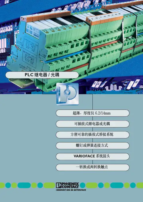
灵活 性意味 着根据 应用场 合既 可以为 每 个通道 自由选 择输入电 压,也可以 装入不 同 的机电式继 电器或者半导 体继电器 (光电 耦 合器) 。固 定的可编程控制 器插件板在这 方 面也是 望尘莫 及。灵活性 也意味着 系统可 以 随时 扩展,并且 可以随 时方便、便 宜地更 换 可插拔式继电器和光电耦合器。
PLC 接口 带回拉式弹簧连接 由 底座接线端子 PLC-BSP…/21 和 可插拔微型继电器组成, 用于安装在 3 上
输入电压 UN
12VDC 24VDC 24VAC/DC 48VDC 60VDC 120VAC/110VDC 230VAC/220VDC2)
12VDC 24VDC 24VAC/DC 48VDC 60VDC 120VAC/110VDC 230VAC/220VDC2)
VARIOFACE 系统接头
(164,)2 mm
可插拔继电器 和光电耦合器,
6.2/14mm
插拔式桥接系统
两个转换 触点 传感器型 执行器型 通用型
按实际应用优化的 系列产品
I
250VAC/6A(10A)
可选用螺钉连接或者回拉式 弹簧连接两种形式
U 通断容量高
一体化集成输入电路 和保护电路
DINVDE0106-101
执行 器 (例如 电磁阀、接 触器等)的 所 有连接线 (包括回线) 都被直接连接在 PLC 执行器接口上。
传感 器 (例 如接 近开 关、限位 开关 等) 的所有连 接线 (包括开 关的供电)都直 接在 PLC 接口上有相应的连接位置。与传统的耦 合元 件相比,可以 节省两 个输出 接线端子 或 者馈 入连接端 子,同时节 省了中 间接线工 作 和宝贵的开关柜空间。
OTM800E4CM230C 电动开关产品说明书
Container Information
Package Level 1 Units Package Level 1 Width Package Level 1 Depth / Length Package Level 1 Height Package Level 1 Gross Weight Package Level 1 EAN
PRODUCT-DETAILS
OTM800E4CM230C OTM800E4CM230C MOTORIZED C/O SWITCH
General Information
Extended Product Type Product ID EAN Catalog Description
Long Description
3650303
Categories
Low Voltage Products and Systems → Switches → Change-over and Transfer Switches → Motorized Change-over Switches
(380 ... 415 V) 800 A (500 V) 800 A (690 V) 800 A
(380 ... 415 V) 720 A
(380 ... 415 V) 650 A
(380 ... 415 V) 450 kW (500 V) 560 kW (690 V) 800 kW q = 40 °C 800 A
Rated Operational Current AC-23A (Ie)
Rated Operational Current AC-31B (Ie) Rated Operational Current AC-33B (Ie) Rated Operational Power AC-23A (Pe)
施耐德E型接触器

选型指南.............................................................................................................. 24 说明,特性 ..........................................................................................................25 热过载继电器选型.............................................................................................27 尺寸及安装 ......................................................................................................... 28
2 根导线
mm2 1...4
1...4
1...4
1...2.5
1...4
软线
1 根导线
mm2 1...4
1...4
1...4
1...2.5
1...4
带接线端子
2 根导线
mm2 1...2.5
1...2.5
1...2.5
1...2.5
1...2.5
硬线
1 根导线
mm2 1...4
1...4
1.5...6
1
选型指南
应用
TeSys® E 接触器
LC1E06到E95
各种类型的控制系统
电子保护断路器系列CT F-Frame 产品说明说明书

The Series C T F-Frame is equipped with the 210+ electronic trip unit and features LSI and LI protection settings. The F-Frame breaker is NEMA T, UL T and CSA T listed.Design flexibility• Three frames cover ampere range from 40 A to 225 A, reducing stock requirements and providing more flexibility than thermal-magnetic breakers• Each trip unit includes seven ampere ratingsand 10 protection profiles• Two protection types, LI and LSI, offer options for adjust-ability and coordination of systemsDesign savings• Uses accessories available on current F-Frame breaker• Same physical dimensions and terminal locations as thermal- magnetic and 310+ electronic F-Frame breakers• Available for aftermarket replacement of any F-Frame when electronic trip units are preferred• Reduced cost from F-Frame 310+ offering of electronic trip unit• Three trip units cover ampere range from 40 A to 225 A, reducing in-house stock and offering more flexibility Easy-to-use 210+ trip unit• Two simple rotary dials adjust settings for amperage and protection levels• Status indication LED notifies the user of operational statusA full range of accessories• In addition to using the same internal accessories as the standard F-Frame, the FDE with 210+ offers various handle locks, plug-in adapters and handle mechanisms• Includes same shunt tripand undervoltage release accessory options as other FD breakers, and the same left-hand side auxiliary and bell alarm contact options • A special 1A/1B auxiliary contact can be installed on the right-hand side; this contact must be factory installed• Uses a functional test kit in common with the 310+ and ACB Digitrip E (MTST230V); a new cable is included in the test kit to test 210+ trip unitsSeries C F-Frame molded-case circuitbreaker with 210+ electronic trip unitFDE 210+ trip unit features• No rating plug required •Factory-installed only; non-interchangeable •Available with LI or LSI protection profiles •Three frames with wide ampere ranges: 40–100 A, 70–150 A and 100–225 A •Fixed long time delay (10 sec at 6 x I r )• Thermal memory •Sealable clear cover to comply with UL and CSA requirements•Optional wire seal for cover (Cat. No. 5108A03H01)•Adjustable short-time delay pickup (LSI): 2–10 x I r•Multiple SD time delayoptions (LSI): INST , 150 ms, 300 ms and I 2t response •Adjustable Instantaneous pickup (LI): 2–12 x I n • Status indicator LED • Push-to-trip button •Optional self-powered plug-in test kit(Cat. No. MTST230V)FDE 210+ ordering guidelinesAvailable featuresA Internal accessories are listed with Underwriters Laboratories (UL) for factory installation. They arenot listed with UL for field installation. Any one internal accessory may be mounted in the left pole. Only a specially built 1A/1B auxiliary switch may be factory mounted in the right pole.FDE, HFDE and FDCE ratings and ampere rangesSpecification Description Breaker typeFDEHFDEFDCE AShort-circuit current ratings (kA rms) AC 50–60 Hz NEMA UL 489240 Vac 65100200480 Vac 3565100600 Vac 182525Number of poles 333Adjustable Long-time pickup CSA 22.2 No. 5225 A A = 100, B = 110, C = 125, D = 150, E = 175, F = 200,G = 225150 A B A = 70, B = 80, C = 90,D = 100,E = 110,F = 125,G = 150100 A A = 40, B = 50, C = 60,D = 70,E = 80,F = 90,G = 100Protection types LI, LSI Dimensions in inches (mm)H W DThree-pole 6.00 (152.4) 4.13 (104.9) 3.38 (85.9)Weight (approximate) lbs (kg) 4.5 (2.0) 4.5 (2.0)4.5 (2.0)A Contact Eaton for availability.B 150 A frame only available in protection style LI.ReferencesDocumentPublication numberTechnical data TD01203013E FAQ MZ01203001ELI trip unit controls LI protection settingsA A S position on 225 A frame set to breakeroverride value of 2400 A.LSI trip unit controlsLSI protection settingsTo learn more, visit /210plusEaton is a registered trademark.All other trademarks are property of their respective owners.Eaton1000 Eaton Boulevard Cleveland, OH 44122United States © 2015 EatonAll Rights Reserved Printed in USAPublication No. PA012010EN / Z16957September 2015Follow us on social media to get the latest product and support information.。
ct MTE低压空气断路器和负荷开关产品简介

多年来,Masterpact 断路器在世界范围内建立了空气断路器技术的新标准,包括技术革新的Micrologic 控制单元,优化的体积尺寸,安全使用的产品特性以及强大的智能通信等附加功能,成为低压配电领域的领导者。
今天,我们以客户价值为出发点,面向多种低压配电系统特别是建筑行业,为客户带来全新的Masterpact MTE 空气断路器。
继承了施耐德电气一贯的优秀品质,Masterpact MTE 将为客户提供更加安全可靠的低压配电保护方案。
额定电流:400A ~4000A● 2种框架规格● Ics =Icu =50/65/85 kA ● 抽屉式/固定式● 3极/ 4极Micrologic 控制单元● MTE MIC 2.0/5.0● MTE MIC 5.0A/6.0A ● MTE MIC 5.0D/6.0D● 负荷开关MTE NA,HA相关认证● 中国强制认证 CCC ● 中国船级认证 CCS标准配置● 电动储能配置● 机械储能配置D: 电能表型A: 电流表型标准型型号包含如下配置 (**)固定式: 断路器本体+控制单元+ 水平接线 (*) +储能马达+ 分励线圈+合闸线圈+ 指示触点+门框 抽屉式: 断路器本体+抽架+控制单元+水平接线 (*) + 储能马达+分励线圈+ 合闸线圈+指示触点+门框+安全挡板+灭弧罩盖MTE 04 N 3 D 20 0(*) 对 MTE40 可以选择垂直接线方式控制回路电压0: 机械储能 (无线圈)2: 电动储能/AC220V 3: 电动储能/AC380V 4: 电动储能/DC220V控制单元:20: MTE Micrologic 2.0二段保护50: MTE Micrologic 5.0三段保护5A: MTE Micrologic 5.0A 三段保护+电流表6A: MTE Micrologic 6.0A 三段保护+电流表+接地故障5D: MTE Micrologic 5.0D 三段保护+功率表6D: MTE Micrologic 6.0D 三段保护+功率表+接地故障00: 负荷开关, 无控制单元型式D: 抽屉式; F: 固定式极数3: 3极; 4: 4极断路器额定电流 (范围:04/400A-40/4000A)断路器分断类型N: 50kA, 65kA; H: 65kA, 85kA; S: 负荷开关断路器类型Masterpact MTE低压空气断路器和负荷开关产品简介AC220VCE 连接 AC380VCD 退出DC220VCT 实验AC220VCE 连接AC380V CD 退出DC220VCT 实验AC220V CE 连接AC380V CD 退出DC220VCT 实验请在方框内 (o ) 打√或填入相应字符断路器 附件 数量 型号 可增 CB EIP PF MNVSPO(*) VBP VSPD VPEC VPOCCCS 加OF 二次 相间 合闸准 失压 位置可编程 本体OFF 按钮锁 抽架退出 抽架门 抽架摇入 接线方式 证书 触点 端子罩 隔板备触点线圈 触点(*****)触点(***)位置锁 定装置位置钥匙锁 联锁联锁 (**)(****)(*) 选择“本体OFF 位置锁”选项后再选择具体“锁芯”的配置。
质粒测序引物(DOC)

p B42ADF p BMN_5' BAC1 p BAD-F p BAD-5' T3/M 13rev p BD-GAL4-F 35S GAL4-Bdfor M 13F/T7 T3/M 13rev T3/M 13rev T3/M 13rev T3/M 13rev PBRforBam p BRforEco PBRforBam PBRforBam GAL4-Bdfor not available T3/M 13rev T7 T3 CM V-Profor,T7 EF-1α Fwd CM V-Profor,T7 p BV220F T7/Tac-Profor
p DSRED-N-R T7/ M 13R T7/ M 13R(距离插入位点合适, 优先安排) M 13R(距离插入位点合适,优 先安排)
p EASY-T 1 p EASY-T 3 p ECFP-N(C) p EF/my c/cyt o/ER/mit o/nuc p EF1(4,6/my c-His) p EF1(4,6/V5-His) p EF1(4;6/His_A;_B;_C) p EF5/FRT /V5-D(-T OPO) p EGFP p EGFP-1 p EGFP-C p EGFP-C1 p EGFP-C2 p EGFP-C3 p EGFP-F p EGFP-N p EGFP-N1 p EGFP-N2 p EGFP-N3 p ENT R p ET -11(-a,-b,-c,-d) p ET -12(-a,-b,-c) p ET -14b p ET -15b p ET -16b p ET -17b p ET -17xb p ET -19b p ET -20b(+) p ET -21(-a,-b,-c,-d)(+) p ET -22b(+) p ET -23(-a,-b,-c,-d)(+) p ET -24(-a,-b,-c,-d)(+) p ET -25b(+) p ET -26b(+) p ET -27b(+) p ET -28a(-b,-c)(+) p ET -29a(-b,-c)(+) p ET -3(-a,-b,-c,-d) p ET -30_Ek/LIC p ET -30_Xa/LIC p ET -30a(-b,-c)(+) p ET -31b(+)
Layer-by-Layer Assembly of Ultrathin Composite Films
Layer-by-Layer Assembly of Ultrathin Composite Films from Micron-Sized Graphite Oxide Sheets andPolycationsNina I.Kovtyukhova,*,†Patricia J.Ollivier,‡Benjamin R.Martin,‡Thomas E.Mallouk,*,‡Sergey A.Chizhik,§Eugenia V.Buzaneva,|andAlexandr D.Gorchinskiy|Institute of Surface Chemistry,National Academy of Sciences of Ukraine,31,Pr.Nauky, 252022Kyiv,Ukraine;Department of Chemistry,The Pennsylvania State University, University Park,Pennsylvania16802;Metal-Polymer Research Institute,32A Kirov Street, Gomel,246652,Belarus;and National T.Shevchenko University,64,Vladimirskaya Str.,252033Kyiv,UkraineReceived November24,1998.Revised Manuscript Received December28,1998Unilamellar colloids of graphite oxide(GO)were prepared from natural graphite and were grown as monolayer and multilayer thin films on cationic surfaces by electrostatic self-assembly.The multilayer films were grown by alternate adsorption of anionic GO sheets and cationic poly(allylamine hydrochloride)(PAH).The monolayer films consisted of11-14Åthick GO sheets,with lateral dimensions between150nm and9µm.Silicon substrates primed with amine monolayers gave partial GO monolayers,but surfaces primed with Al13O4-(OH)24(H2O)127+ions gave densely tiled films that covered approximately90%of the surface. When alkaline GO colloids were used,the monolayer assembly process selected the largest sheets(from900nm to9µm)from the suspension.In this case,many of the flexible sheets appeared folded in AFM images.Multilayer(GO/PAH)n films were invariably thicker than expected from the individual thicknesses of the sheets and the polymer monolayers,and this behavior is also attributed to folding of the sheets.Multilayer(GO/PAH)n and(GO/ polyaniline)n films grown between indium-tin oxide and Pt electrodes show diodelike behavior,and higher currents are observed with the conductive polyaniline-containing films. The resisitivity of these films is decreased,as expected,by partial reduction of GO to carbon.IntroductionThe assembly of composite thin films from lamellar inorganic particles and organic macromolecules is an inexpensive and versatile route to functional nanometer-scale structures.1These films are grown by a wet chemical,layer-by-layer adsorption method,which is similar to that developed earlier by Decher and co-workers for organic polyelectrolytes.2The addition of inorganic components offers the possibility of added optical,electronic,magnetic,mechanical,and thermal properties that may be difficult to achieve by using organic polymers alone.Additionally,the continuous inorganic sheets provide a barrier to interpenetration of sequentially deposited polymer or nanoparticle layers, a feature that can be important in thin films intended to act as current rectifiers,photodiodes,or Coulomb blockade devices.Several electronic and photonic ap-plications along these lines have established the utility of this method.3The layer-by-layer assembly method relies on the exfoliation of solids to produce colloids of sheets,which typically have nanometer thicknesses and lateral di-mensions of tens of nanometers to microns.Exfoliation procedures based on ion exchange and redox reactions have been developed for a variety of lamellar solids.4 Thus,multilayer inorganic/organic films have been grown from lamellar metal phosphates,titanates,nio-bates,5silicates,1b and metal chalcogenides,6compounds which in bulk form possess transport properties ranging from insulating to semimetallic.Recently,Fendler and co-workers have shown that such films can also be†National Academy of Sciences of Ukraine.‡The Pennsylvania State University.§Metal-Polymer Research Institute.|National T.Shevchenko University.(1)(a)Iler,R.K.J.Colloid Interface Sci.1966,21,569.(b)Kleinfeld,E.R.;Ferguson,G.S.Science1994,265,370.(c)Fendler,J.H.; Meldrum,F.Adv.Mater.1995,7,607.(d)Mallouk,T.E.;Kim,H.-N.; Ollivier,P.J.;Keller,S.W.In Comprehensive Supramolecular Chemistry;Alberti,G.,Bein,T.,Eds.;Elsevier Science;Oxford,UK, 1996;Vol.7,pp189-218.(2)Decher,G.Science1997,277,1232.(3)(a)Kaschak,D.M.;Mallouk,T.E.J.Am.Chem.Soc.1996,118, 4222.(b)Feldheim,D.L.;Grabar,K.C.;Natan,M.J.;Mallouk,T.E. J.Am.Chem.Soc.1996,118,7640.(c)Keller,S.W.;Johnson,S.A.; Yonemoto,E.H.;Brigham,E.S.;Mallouk,T.E.J.Am.Chem.Soc. 1995,117,12879.(d)Cassagneau,T.;Mallouk,T.E.;Fendler,J.H.J. Am.Chem.Soc.1998,120,7848.(4)(a)Jacobson,A.J.Mater.Sci.Forum1994,152-153,1.(b) Jacobson,A.J.In Comprehensive Supramolecular Chemistry;Alberti, G.,Bein,T.,Eds.;Elsevier Science;Oxford,UK,1996;Vol.7,pp315-335.(5)(a)Keller,S.W.;Kim,H.-N.;Mallouk,T.E.J.Am.Chem.Soc. 1994,116,8817.(b)Fang,M.,Kim,C.-H.;Saupe,G.B.;Kim,H.-N.; Waraksa,C.C.;Miwa,T.;Fujishima,A.;Mallouk,T.E.Submitted to Chem.Mater.(6)Ollivier,P.J.;Kovtyukhova,N.I.;Keller,S.W.;Mallouk,T.E. J.Chem.Soc.,mun.1998,1563.771Chem.Mater.1999,11,771-77810.1021/cm981085u CCC:$18.00©1999American Chemical SocietyPublished on Web01/28/1999grown from graphite oxide(GO),7which can subse-quently be reduced electrochemically to make electroni-cally conducting graphitic films.In their work,GO nanoparticles were prepared from synthetic graphite. They noted that the multilayer films consisted of incompletely exfoliated platelets that were tens of nanometers in their lateral dimensions.In this paper, we revisit the assembly of GO/polycation thin films, using GO prepared from natural crystals.We show that exfoliated GO derived from these crystals is a mechani-cally robust material that deposits conformally on cationic surfaces as micron-sized,nanometer-thick sheets. Graphite oxide is a pseudo-two-dimensional solid in bulk form,with strong covalent bonding within the layers.Weak interlayer contacts are made by hydrogen bonds between intercalated water molecules.8-11The carbon sheets in GO contain embedded hydroxyl and carbonyl groups,as well as carboxyl groups situated mainly at the edges of the sheets.8,9,12While there is no consensus as to the precise structure of GO layers, different structural models,9a,b,10which correspond to an ideal formula of C8O2(OH)2,have been advanced.A recent study of the structure of GO argues from13C and 1H NMR evidence for the presence of epoxy groups.13 Nakajima and co-workers have proposed that the carbon layers in GO are linked together in pairs by sp3C-C bonds perpendicular to the sheets.10According to Kli-nowski et al.,13the carbon layers in GO contain two kinds of domains,aromatic regions with unoxidized benzene rings and aliphatic regions with six-membered carbon rings.The relative size of the domains,which are randomly distributed,depends on the degree of oxidation.In both models,the hydroxyl groups project above and below the carbon grid.The phenolic hydroxyl groups are acidic and,together with the carboxyl groups, are responsible for the negative charge on the GO sheets in aqueous suspensions.9,13The surface charge density of colloidal GO particles(degree of oxidation85%)was measured by Fendler and co-workers as0.4per100Å2.7 The GO interlayer distance is not constant and depends strongly on the GO:H2O ratio.8-10,15In very dilute aqueous suspensions,the interlayer distance is large,so interaction between the layers is sufficiently weak that exfoliation occurs.8Our previous research showed that the number of layers in the GO colloidal particles can be controlled by the dilution of the suspen-sions.16,17The adsorption capacity for Cu(II)ions,which was for both aqueous suspensions16and thin films deposited from these suspensions on powder supports (ZnO,Al2O3,fumed SiO2),17increased with decreasing GO concentration in the starting suspension.For ex-ample,the adsorption capacity of GO films on SiO2 increased by a factor of2.4when the GO concentration in the starting suspension was decreased from1.0to 0.3g/L.This result shows that more complete exfoliation provides increased access to the GO functional groups. For samples prepared from the colloids with GO con-centrations of0.02-0.3g/L,the maximum adsorption capacity,22-24mmol/g,was obtained.This value is close to the total quantity of oxygen-containing groups in GO(25mmol/g9)and gives indirect evidence that dilute GO colloids are exfoliated as monolayers.We report here a detailed study of the preparation and characterization of GO/polycation films grown on planar Si and Al2O3/Al ing atomic force microscopy(AFM),ellipsometry,and electrical mea-surements,the following questions have been addressed: What does the first layer of the sheets adsorbed on a substrate look like microscopically?Can we affect the quality of mono-and multilayer films by varying the conditions of their deposition and the chemical composition of the substrate surface? What are the electronic properties of GO/polycation films,and how are they influenced by the nature of the polycation?Experimental SectionMaterials.GO was synthesized from natural graphite powder(325mesh,GAK-2,Ukraine)by the method of Hum-mers and Offeman.18It was found that,prior to the GO preparation according to ref18,an additional graphite oxida-tion procedure was needed.Otherwise,incompletely oxidized graphite-core/GO-shell particles were always observed in the final product.The graphite powder(20g)was put into an80°C solution of concentrated H2SO4(30mL),K2S2O8(10g),and P2O5(10g).The resultant dark blue mixture was thermally isolated and allowed to cool to room temperature over a period of6h.The mixture was then carefully diluted with distilled water,filtered,and washed on the filter until the rinse water pH became neutral.The product was dried in air at ambient temperature overnight.This preoxidized graphite was then subjected to oxidation by Hummers’method.The oxidized graphite powder(20g)was put into cold(0°C)concentrated H2SO4(460mL).KMnO4(60g)was added gradually with stirring and cooling,so that the temperature of the mixture was not allowed to reach20°C.The mixture was then stirred at35°C for2h,and distilled water(920mL)was added.In 15min,the reaction was terminated by the addition of a large amount of distilled water(2.8L)and30%H2O2solution(50 mL),after which the color of the mixture changed to bright yellow.The mixture was filtered and washed with1:10HCl solution(5L)in order to remove metal ions.The GO product was suspended in distilled water to give a viscous,brown,2% dispersion,which was subjected to dialysis to completely remove metal ions and acids.The resulting0.5%w/v GO dispersion,which is stable for a period of years,was used to prepare exfoliated GO.Exfoliation was achieved by dilution of the0.5%GO disper-sion(1mL)with deionized water(24mL),followed by15min sonication.The resulting homogeneous yellow-brown sol, which contained0.2g/L GO,was stable for a period of months and was used for film preparation.An aqueous solution(0.01M)of poly(allylamine hydrochlo-ride),PAH,(Aldrich,MW)50000-65000)was adjusted to pH7with NH3and was used for growth of polycation layers.(7)(a)Kotov,N.A.;Dekany,I.;Fendler,J.H.Adv.Mater.1996,8,637.(b)Cassagneau,T.;Fendler,J.H.Adv.Mater.1998,10,877.(8)(a)Thiele,H.Kolloid-Z1948,111,15.(b)Croft,R.C.Quart.Rev.1960,14,1.(9)(a)Scholz,W.;Boehm,H.P.Z.Anorg.Allg.Chem.1969,369,327.(b)Clauss,A.;Boehm,H.P.;Hofmann,U.Z.Anorg.Allg.Chem.1957,291,205.(10)Nakajima,T.;Mabuchi,A.;Hagiwara,R.Carbon1988,26,357.(11)Karpenko,G.;Turov,V.;Kovtyukhova,N.;Bakai,E.;Chuiko,A.Theor.Exp.Chem.(Russ.)1990,1,102.(12)Hadzi,D.;Novak,A.Trans.Faraday.Soc.1955,51,1614.(13)Lerf,A.;He,H.;Forster,M.;Klinowski,J.J.Phys.Chem.B1998,102,4477.(14)Hennig,Z.Progr.Inorg.Chem.1959,1,125.(15)Lagow,R.J.;Badachhape,R.B.;Wood,J.L.;Margrave,J.L.J.Chem.Soc.Dalton1974,1268.(16)Kovtjukhova,N.I.;Karpenko,G.A.Mater.Sci.Forum1992,91-93,219.(17)(a)Kovtyukhova,N.I.;Chuiko,A.A.Abstracts;Fall Meetingof the Materials Research Society,1994,Boston,C9.6.(b)Kovtyukhova,N.I.;Buzaneva,E.V.;Senkevich,A.Carbon1998,36,549.(18)Hummers,W.;Offeman,R.J.Am.Chem.Soc.1958,80,1339. 772Chem.Mater.,Vol.11,No.3,1999Kovtyukhova et al.An aqueous solution of doped polyaniline(PAN)was made from a saturated solution of the emeraldine base form in dimethylformamide.A3mL portion of this solution was slowly added with stirring to26mL of water,which had been acidified to pH3.5with aqueous HCl.The pH of the final PAN solution was then adjusted to2.5by addition of aqueous HCl.The alu-minum Keggin ion Al13O4(OH)24(H2O)127+was prepared trom Al13O4(OH)25(H2O)11(SO4)3‚x(H2O),which was available from a previous study.5Briefly,0.102g of the sulfate salt was added to a solution of0.042g of BaCl2in200mL of water and stirred overnight.The resulting0.3mM solution of the chloride salt of the aluminum Keggin ion was filtered using a0.2µm filter.Polished(100)Si wafers were sonicated in CCl4for15min and then rinsed with2-propanol and water.Their surface was then hydroxylated by30min sonication in“piranha”solution (4:1concentrated H2SO4:30%H2O2)(CAUTION:piranha solution reacts violently with organic compounds!)and was rinsed sequentially with water,methanol,and1:1methanol/ toluene before the surface derivitization steps began.Aluminum foil,Al-coated glass,both bearing a native oxide, and ITO glass were cleaned by washing with hexane for15 min prior to GO adsorption.Multilayer GO/PAH Film Growth.Hydroxylated silicon wafers were primed with one of three different types of cationic monolayers in order to initiate the growth of the GO films. This was achieved either by(1)reacting with4-((dimethyl-methoxy)silyl)butylamine(15h treatment with a5%toluene solution under dry Ar,over KOH at ambient temperature)or by(2)adsorbing a monolayer of aluminum Keggin ions(5min adsorption from aqueous solution of the chloride salt at80°C19) or by(3)adsorbing PAH(15min adsorption from a0.01M aqueous solution at pH7and ambient temperature).The primed Si substrates(1,2,and3)are designated hereafter as Si(NH2),Si(OH)/Al-Kg,and Si(OH)/PAH,respectively.The primed substrates were immersed in an aqueous(pH 5)or aqueous ammonia(pH9)GO sol(0.2g/L)for15min and then rinsed with deionized water and dried in flowing Ar.The samples were then immersed in aqueous PAH solutions for 15min,rinsed with deionized water,and dried in flowing Ar. Multilayer GO/PAH films were grown by repeating these adsorption cycles.Preliminary experiments had shown that the thickness of a deposited layer(estimated by ellipsometry) does not depend on the substrate/solution contact time in the range from2min to2h.For electronic measurements, multilayer(GO/PAH)14and(GO/PAN)30films were grown on ITO in similar adsorption cycles.For comparison purposes,a GO colloid film(ca.90nm thick)was prepared by dip-coating the ITO/glass in the GO colloidal dispersion.Characterization.Atomic force microscopy(AFM)images of the layers deposited on Si substrates were obtained with a Digital Instruments Nanoscope IIIa in tapping mode,using a 3045JVW piezo tube scanner.The125µm etched Si cantile-vers had a resonant frequency between250and325kHz,and the oscillation frequency for scanning was set to∼0.1-3kHz below resonance.Typical images were obtained with line scan rates of2Hz while256×256pixel samples were collected.Ellipsometric measurements were made with a Gaertner model L2W26D ellipsometer.An analyzing wavelength of632 nm was used,because GO absorbs minimally at this wave-length.The incident angle was70°and the polarizer was set at45°.Ellipsometric parameters were measured following each GO or PAH adsorption step.Si substrates were dried in an Ar stream before each measurement.The film thickness of the GO/PAH multilayers was calculated using the Si refractive indices,n s)3.875and k s)-0.018,determined from a blank sample.The refractive index of GO/PAH films was estimated as n f)1.540,k f)0.Transmission electron microscope(TEM)images were ob-tained with a JEOL1200EXII microscope at120kV ac-celerating voltage.Samples were prepared by immersing a copper grid in the GO sol and drying in air.The elemental composition of GO was determined by using a home-built mass spectrometer with laser probe(LMS).The diameter of the crater for single laser impulse was0.42-0.48 mm,and the depth was1µm.IR spectra were recorded using a Perkin-Elmer325instrument.XPS spectra were obtained using a Kratos Series800spectrometer with hν)1253.6eV and an analyzing window of4×6mm2.The accuracy of the measured core level binding energies(E b)was0.1eV.For LMS, IR,and XPS experiments,GO samples were prepared as films by drying a droplet of the sol in air at ambient temperature. X-ray powder diffraction(XRD)patterns were recorded with a DRON-1instrument using Cu K R radiation.Prior to the measurement,the GO sample was dried in a vacuum over P2O5 for24h.Electrical measurements of films deposited on ITO glass were carried out using top Pt electrode contacts that were10µm in diameter and mechanically pressed into the film,usinga home-built parametric analyzer.The sensitivity of current measurements was0.01nA.All measurements were carried out in air at ambient temperature.The turn-on potential for all thin film devices studied was taken as the potential at which a current of1.0nA was observed.In regions where current was more than3nA,every step of voltage increase (typically0.1mV in both the forward and reversed directions) was followed by repeating the measurement cycle to ensure the reproducibility of the current measured at the lower voltage.Measurements were considered irreversible(i.e.,a permanent change to a more conductive state occurred)when the current recorded the second time at the lower voltage was noticeably higher than that measured in the previous cycle.Results and Discussion Characterization of the GO Colloid.The XRD pattern of GO prepared by preoxidation with persulfate followed by oxidation with permanganate reveals a sharp002reflection at2θ)12.80°,which corresponds to a c-axis spacing of6.91ÅThis value falls within the range of6.3-7.7Åreported in the literature9a,10,20,21for GO prepared from natural graphite according to Hum-mers’method.18No002diffraction peak from unreacted graphite(d)3.35Å)is observable in the XRD pattern. The IR spectrum of GO prepared by this method is essentially identical to that reported in the litera-ture.9a,12,21A band at3420cm-1and a broad band centered around3220cm-1are attributed to O-H stretching vibrations of the C-OH groups and water, respectively;a band at1730cm-1is assigned to C d O stretching vibrations of the carbonyl and carboxyl groups.Bands at1365,1425,and1615cm-1are assigned to the O-H deformations of C-OH groups and water,respectively.A band at1080cm-1is due to C-O stretching vibrations.Deconvolution of the C1s peak in the XPS spectrum shows the presence of four types of carbon bonds:C-C (284.8eV),C-O(286.2eV),C d O(287.7eV),and O-C d O(288.5eV).By integrating the area of the deconvolu-tion peaks,the following approximate percentages were obtained:C-C,49.5;C-O,31.4;C d O,9.1;O-C d O, 2.9.The LMS spectrum of GO prepared by this method gave the following atomic composition(wt%):H,2.3; C,45.2;O,46.5;P,3.3;K,2.7;C:O ratio)1.3.The same or nearly the same C:O ratio has been found previously for GO samples prepared from natural graphite.21,22It is generally accepted that the conversion of graphite to(19)Schoenherr,S.;Goerz,G.;Mueller,D.;Gessner,W.Z.Anorg. Allg.Chem.1981,476,188.(20)Carr,K.E.Carbon1970,8,245.(21)Kyotani,T.;Suzuki,K.;Yamashita,H.;Tomita,A.Tanso1993, 160,255.(22)Slabaugh,W.H.;Seiler,B.C.J.Phys.Chem.1962,66,396.Assembly of Ultrathin Composite Films Chem.Mater.,Vol.11,No.3,1999773GO is complete when the C:O ratio becomes 2.0.The observed ratio C:O:H )4:3.1:2.5is richer in O and H than that calculated for C 8O 2(OH)2:4:2:1;this can be explained by the presence of intercalated/adsorbed water and carboxyl groups,as shown by IR and XPS.It should be noted that the ideal formulation does not take into account the presence of carboxyl groups,which are mainly situated on the edges of the sheets,8or interca-lated water,some amount of which is probably an integral part of the GO structure.3Allowing that 2.9%of the carbon atoms are present as carboxyl groups (from XPS)and assuming that the potassium ions are incor-porated by ion-exchange,we calculate a formula of C 3.77O 2.05H 0.92K 0.07‚0.73H 2O,or C 8O 2.25(OH)1.95(OK)0.15‚1.55H 2O,which gives a C:O:H ratio of 4:2.95:2.5.The remaining oxygen (2.05wt %)is most probably bound to phosphorus,an impurity introduced by the graphite preoxidation step.TEM images of the GO sol (Figure 1)reveal flexible,wrinkled sheets of different lateral sizes ranging from hundreds to thousands of nanometers.Flexible GO particles were also observed by Hennig and Carr.14,20No graphite particles are observed in these images.AFM Images of the First Adsorbed GO Layer.Si Substrates.AFM images (Figure 2a -c)of the GO films deposited in one adsorption cycle from aqueous solution show surface coverages of about 30%for Si(NH 2),85%for Si(OH)/PAH,and 90%for Si(OH)/Al-Kg substrates.The main features are 150-900-nm-wide islands,whose size is close to that determined by TEM for the GO sheets.In some cases,corrugations and the turned-in edges of the sheets are seen.For the PAH-primed Si substrate,the average roughness of the sheet-coveredpart of the surface is 4.5ÅBy comparison,the rough-ness of the Si(OH)/PAH substrate was 6.2-Å,indicating slight smoothing of the surface by the GO monolayer.The height of the islands on Si(NH 2)and Si(OH)/PAH,10.6-14.1Å,and the average roughness of their surface,3.9-4.5Å,are consistent with exposure of GO basal planes covered by adsorbed H 2O.8-10Ellipsometric measurements gave 11and 14Åthicknesses for GO monolayers on Si(NH 2)and Si(OH)/PAH.Considering that the thickess of the priming layer is about 7Å,and that the GO sheets cover only part of the surface,these results are in reasonable agreement with the island heights measured by AFM.According to Nakajima’s structural model,10the thick-ness of a GO monolayer depends on the content of hydroxyl groups on its basal planes and can reach 8.2Åfor the completely hydroxylated monolayer.Assuming the presence of completely hydroxylated GO carbon layers in very dilute colloids,one can take the thickness of a GO monolayer as 8.2Å.By comparing this value with the height of the islands in Figure 2,one can conclude that the islands consist of a single GO sheet covered by a layer of adsorbed water molecules.The thickness of doubled GO layers can be estimated from the thickness of two GO monolayers,2×8.2Å,plus the distance between the layers,which is determined by the thickness of the layer of weakly bound mobile water molecules.11,13This interlayer distance can be estimated at about 3Å,from the repeat distance along the c -axis of well-hydrated GO samples,I c )11Å,9,14minus the thickness of a GO monolayer,8.2Å.This means the thickness of doubled GO layers should be about 20Åor more,if water adsorbed onto the top basal plane is considered.This value is significantly greater than the height of adsorbed islands (10.6-14.1Å).The height,20.1Å,of the GO islands adsorbed onto the Al-Keggin-primed Si surface (Figure 2b)is roughly consis-tent with the thickness of the Al-Keggin anchoring layer (7Å23)and a monolayer of GO sheets covered by adsorbed H 2O (10.6-14.1Å).An AFM image of the first GO layer adsorbed from an aqueous ammonia suspension (pH 9)onto a Si(NH 2)substrate is shown in Figure 2d.In this case,the adsorption process selects much larger sheets (900-9000nm)which cover about 60-65%area of the surface.The dissociation of the GO hydroxyl groups (situated mainly on the basal planes)occurs around pH 9and significantly increases the negative charge density on the GO sheets.The increased attraction of the sheets for the cationic surface results in higher coverage than that observed at lower pH.This interaction is appar-ently more effective for the larger sheets,which can bridge over neutral regions of the incompletely primed surface.Previous studies have shown that the amine priming layer does not completely cover the surface,and that it is only partially protonated at pH 9.5The average roughness of the sheets on the surface is 4.4Å.The height of the sheets,which are corrugated and some-times have turned-in edges,is in the range of 19-23Å.The increased thickness may be due to a hydrated layer of charge-compensating NH 4+ions,which cover the basal plane surface.The adsorption of a bilayer of sheets(23)Johansson,G.;Lundgren,G.;Sillen,L.G.;Soderquist,R.Acta Chem.Scand.1960,14,769.Figure 1.Transmission electron micrograph of colloidal graphite oxide particles.774Chem.Mater.,Vol.11,No.3,1999Kovtyukhova et al.seems unlikely,since in basic media the exfoliation of GO occurs more readily.8Al 2O 3/Al Substrates.AFM images of the first GO layer grown on Al-coated glass (Figure 3a)and alumi-num foil (not shown)resemble those of the substrates,except that corrugations similar to those seen in the TEM image of GO and AFM images of the GO/Si have appeared.Because both Al 2O 3/Al substrates are very rough and because the flexible GO sheets conform to the surface,it is not possible to determine the lateral and vertical dimensions of the sheets.However,the average roughness of the brighter area in the image,which is presumed to have an adsorbed GO sheet,is 2.7nm.By comparison,the substrate roughness is 3.5-nm,again indicating a slight smoothing of the surface by the GO sheets.Characterization of GO/PAH Multilayers.Ellipsometry.Figure 4shows plots of film thickness,determined by ellipsometry,versus the number of adsorption cycles for GO/PAH multilayer films.The films were grown on Si(NH 2),Si(OH)/PAH,and Si(OH)/Al-Kg substrates.The linearity of the filmthicknessFigure 2.Tapping-mode AFM images of the first graphite oxide layer deposited from aqueous and aqueous ammonia sols on primed Si substrates:(a)Si(NH 2),GO sol pH 5,with the linescan showing the apparent height of sheet (14Å)above the background;(b)Si(OH)/Al-Kg,GO sol pH 5;(c)Si(OH)/PAH,GO sol pH 5;and (d)Si(NH 2),GO sol pH 9.Assembly of Ultrathin Composite Films Chem.Mater.,Vol.11,No.3,1999775plots indicates that on average the same amount of material is deposited in each adsorption cycle.However,for each the sample,the average increase in layer thickness per PAH/GO bilayer is different and ranges from 29to 50Å(Table 1).The lowest value,29Åper PAH/GO bilayer,is found for GO grown from aqueous ammonia solution (pH 9).The smaller layer pair thick-ness in this case may arise from partial deprotonation of the underlying PAH layer at this pH.Because thesurface charge density is lower,fewer anionic sheets are bound by the polymer per unit area.It should be noted that the measured thickness of the GO/PAH layer pair (40-50Å)is more than that expected from the thickness of monolayer GO sheets (10.6-14.1Å,as estimated by AFM for the first depos-ited GO layer,Figure 2a -c)and the thickness of single PAH layer (5Å24).This can be explained in part by folding of the flexible GO sheets,which is apparent in the AFM images of all GO monolayers except the low coverage layer grown on Si(NH 2).The multilayer ad-sorption model proposed by Kleinfeld and Ferguson for clay/polycation films 1b may also be operative for GO/PAH.In their model,each adsorption cycle deposits about two layers of polyelectrolyte,but they rearrange (possibly by folding in the present case)into alternating single sheet/polycation films.A plot of the thickness of a GO/PAH film grown from aqueous solution onto Si(NH 2)is linear only after the third cycle.The average increase in thickness per PAH/GO bilayer is 23Åin the first two adsorption cycles and 49Åin the following three adsorption cycles (Figure 4).This behavior is reminiscent of that observed by Kleinfeld and Ferguson for clay/polycation films,which nucleate in islands and completely cover the surface only after several adsorption cycles.25We conclude that the GO/PAH film coverage is relatively complete after adsorption of the second bilayer (the first adsorption cycle covers ∼30%of the surface;Figure 2a).In subse-quent adsorption cycles,the layer pair thickness is close to that found for GO/PAH multilayers on Si(OH)/PAH.In the latter case,the surface coverage is ∼85%after the first adsorption cycle,as shown in Figure 2c.AFM.AFM images of four or five bilayer GO/PAH films on all three substrates were similar and did not clearly resolve the sheet edges or the voids between sheets.From these images,one can only conclude that the multilayer films completely cover the surface.Figure 3b shows a typical image of a Si(OH)/Al-Kg /(GO/PAH)3GO film.The average roughness of this film is 20Å,which is consistent with a surface of loosely tiled and folded sheets.Multilayer film roughness and thick-ness parameters,determined by AFM and ellipsometry,respectively,are summarized in Table 1.For all the substrates under investigation (except for very rough aluminum foil),GO/PAH multilayers depos-ited from aqueous sols on Al(OH)x -terminated surfaces (Si(OH)/Al-Kg and Al/Al 2O 3)are smoother than those deposited on NH 2-terminated surfaces (Si(NH 2)and Si-(OH)/PAH)(Table 1).Comparing the surface morphol-ogies of the first GO layer and the multilayer films,one can see that the more densely tiled first layer (∼90%,Figure 2b),grown on the Keggin-primed surface,yields a smoother and more compact multilayer film,whereas the poorly tiled first layer (∼35%,Figure 2a)on Si(NH 2)yields the roughest multilayer surface.Again,this behavior is consistent with the model proposed by Kleinfeld and Ferguson for multilayer growth on is-lands,which eventually coalesce into smoother films.25(24)(a)Lvov,Yu.;Haas,H.;Decher,G.;Mohwald,H.;Kalachev,A.J.Phys.Chem.1993,97,12835.(b)Lvov,Yu.;Decher,G.;Mohwald,ngmuir 1993,9,481,(c)Decher,G.;Hong,J.;Schmitt,J.Thin Solid Films 1992,210/211.(25)Kleinfeld,E.R.;Ferguson,G.R.Chem.Mater.1996,8,1575.Figure 3.(a)Tapping-mode AFM image of the first graphite oxide layer deposited from the aqueous sol onto Al-coated glass and (b)image of a (GO/PAH)3GO film on Si(OH)/Al-Kg.Z range is 15nm in bothimages.Figure 4.Ellipsometric measurements of the thickness of multilayer GO/PAH films vs number of adsorption cycles:1,Si(OH)/PAH(GO/PAH)n GO;2,Si(OH)/Al-Kg(GO/PAH)n GO;3,Si(NH 2)(GO/PAH)n GO;4,Si(NH 2)(GO/PAH)n GO (pH 9).The thicknesses at an abscissa value of 0.5correspond to primer cationic layers;points on the plots refer to films terminated by a GO layer.776Chem.Mater.,Vol.11,No.3,1999Kovtyukhova et al.。
发那科地址一览表
地址一览表MT→PMCT系列M系列PMC→CNCG000ED7ED6ED5ED4ED3ED2ED1ED0G001ED15ED14ED13ED12ED11ED10ED9ED8G002ESTB EA6EA5EA4EA3EA2EA1EA0G004MFIN3MFIN2FING005BFIN AFL BFIN TFIN SFIN EFIN MFING006SKIPP OVC*ABSM SRNG007RLSOT EXLM*FLWU RLSOT3ST STLKG008ERS RRW*SP*ESP*BSL*CSL*ITG009PN16PN8PN4PN2PN1G010*JV7*JV6*JV5*JV4*JV3*JV2*JV1*JV0G011*JV15*JV14*JV13*JV12*JV11*JV10*JV9*JV8G012*FV7*FV6*FV5*FV4*FV3*FV2*FV1*FV0G014ROV2ROV1G016F1D MSDFONG018HS2D HS2C HS2B HS2A HS1D HS1C HS1B HS1AG019RT MP2MP1HS3D HS3C HS3B HS3AG024EPN7EPN6EPN5EPN4EPN3EPN2EPN1EPN0G025EPNS EPN13EPN12EPN11EPN10EPN9EPN8G027CON*SSTP3*SSTP2*SSYP1SWS3SWS2SWS1G028PC2SLC SPSTP*SCPF*SUCPF GR2GR1G029*SSTP SOR SAR GR21G030SOV7SOV6SOV5SOV4SOV3SOV2SOV1SOV0G032R08I R07I R06I R05I R04I R03I R02I R01IG033SIND SSIN SGN R12I R11I R10I R09IG034R08I2R07I2R06I2R05I2R04I2R03I2R02I2R01I2G035SIND2SSIN2SGN2R12I2R11I2R10I2R09I2G036R08I3R07I3R06I3R05I3R04I3R03I3R02I3R01I3G037SIND3SSIN3SGN3R12I3R11I3R10I3R09I3G038*BECLP*BEUCP SPPHS SPSYCG039GOQSM WOQSM OFN5OFN4OFN3OFN2OFN1OFN0G040WOSET PRC S2TLSG041HS2ID HS2IC HS2IB HS2IA HS1ID HS1IC HS1IB HS1IAG042DMMC HS3ID HS3IC HS3IB HS3IAG043ZRN DNC1MD4MD2MD1G044MLK BDT1G045BDT9BDT8BDT7BDT6BDT5BDT4BDT3BDT2G046DRN KEY4KEY3KEY2KEY1SBKG047TL128TL64TL32TL16TL08TL04TL02TL01G048TLRST TLRST1TLSKP TL256G049*TLV7*TLV6*TLV5*TLV4*TLV3*TLV2*TLV1*TLV0 G050*TLV9*TLV8 G053CDZ SMZ UINT TMRON G054UI007UI006UI005UI004UI003UI002UI001UI000 G055UI015UI014UI013UI012UI011UI010UI009UI008 G058EXWT EXSTP EXRD MINP G060*TSBG061RGTSP2RGTSP1RGTAP G062RTNT*CRTOFG063NOZAGCG066EKSET ENBKY IGNVRY G070MRDYA ORCMA SFRA SRVA CTH1A CTH2A TLMHA TLMLA G071RCHA RSLA INTGA SOCNA MCFNA SPSLA*ESPA ARSTA G072RCHHGA MFNHGA INCMDA OVRA DEFMDA NRROA ROTAA INDXA G073DSCNA MPOFA SLVA MORCMA G074MRDYB ORCMB SFRB SRVB CTH1B CTH2B TLMHB TLMLB G075RCHB RSLB INTGB SOCNB MCFNB SPSLB*ESPB ARSTB G076RCHHGB MFNHGB INCMDB OVRB DEFMDB NRROB ROTAB INDXB G077DSCNB MPOFB SLVB MORCMB G078SHA07SHA06SHA05SHA04SHA03SHA02SHA01SHA00 G079SHA11SHA10SHA09SHA08 G080SHB07SHB06SHB05SHB04SHB03SHB02SHB01SHB00 G081SHB11SHB101SHB09SHB08 G082Reserved for order-made macroG083Reserved for order-made macroG091SRLN13SRLN12SRLN11SRLN10 G092BGEN BGIALM BGION IOLS IOLACK G096HROV*HROV6*HROV5*HROV4*HROV3*HROV2*HROV1*HROV0 G098EKC7EKC6EKC5EKC4EKC3EKC2EKC1EKC0 G100+J4+J3+J2+J1 G102-J4-J3-J2-J1 G106MI4MI3MI2MI1 G108MLK4MLK3MLK2MLK1 G110+LM4+LM3+LM2+LM1 G112-LM4-LM3-LM2-LM1 G114*+L4*+L3*+L2*+L1 G116*-L4*-L3*-L2*-L1 G118*+ED4*+ED3*+ED2*+ED1 G120*-ED4*-ED3*-ED2*-ED1 G125IUDD4IUDD3IUDD2IUDD1 G126SVF4SVF3SVF2SVF1 G130*IT4*IT3*IT2*IT1 G132+MIT4+MIT3+MIT2+MIT1 G134-MIT4-MIT3-MIT2-MIT1 G136EAX4EAX3EAX2EAX1 G138SYNC4SYNC3SYNC2SYNC1 G140SYNCJ4SYNCJ3SYNCJ2SYNCJ1 G142EBUFA ECLRA ESTPA ESOFA ESBKA EMBUFA ELCKZA EFINA G143EMSBKA EC6A EC5A EC4A EC3A EC2A EC1A EC0AG144EIF7A EIF6A EIF5A EIF4A EIF3A EIF2A EIF1A EIF0AG145EIF15A EIF14A EIF13A EIF12A EIF11A EIF10A EIF9A EIF8AG146EID7A EID6A EID5A EID4A EID3A EID2A EID1A EID0AG147EID15A EID14A EID13A EID12A EID11A EID10A EID9A EID8AG148EID23A EID22A EID21A EID20A EID19A EID18A EID17A EID16AG149EID31A EID30A EID29A EID28A EID27A EID26A EID25A EID24AG150DRNE RTE OVCE ROV2E ROV1EG151*FV7E*FV6E*FV5E*FV4E*FV3E*FV2E*FV1E*FV0EG154EBUFB ECLRB ESTPB ESOFB ESBKB EMBUFB ELCKZB EFINBG155EMSBKB EC6B EC5B EC4B EC3B EC2B EC1B EC0BG156EIF7B EIF6B EIF5B EIF4B EIF3B EIF2B EIF1B EIF0BG157EIF15B EIF14B EIF13B EIF12B EIF11B EIF10B EIF9B EIF8BG158EID7B EID6B EID5B EID4B EID3B EID2B EID1B EID0BG159EID15B EID14B EID13B EID12B EID11B EID10B EID9B EID8BG160EID23B EID22B EID21B EID20B EID19B EID18B EID17B EID16BG161EID31B EID30B EID29B EID28B EID27B EID26B EID25B EID24BG166EBUFC ECLRC ESTPC ESOFC ESBKC EMBUFC ELCKZC EFINCG167EMSBKC EC6C EC5C EC4C EC3C EC2C EC1C EC0CG168EIF7C EIF6C EIF5C EIF4C EIF3C EIF2C EIF1C EIF0CG169EIF15C EIF14C EIF13C EIF12C EIF11C EIF10C EIF9C EIF8CG170EID7C EID6C EID5C EID4C EID3C EID2C EID1C EID0CG171EID15C EID14C EID13C EID12C EID11C EID10C EID9C EID8CG172EID23C EID22C EID21C EID20C EID19C EID18C EID17C EID16CG173EID31C EID30C EID29C EID28C EID27C EID26C EID25C EID24CG178EBUFD ECLRD ESTPD ESOFD ESBKD EMBUFD ELCKZD EFINDG179EMSBKD EC6D EC5D EC4D EC3D EC2D EC1D EC0DG180EIF7D EIF6D EIF5D EIF4D EIF3D EIF2D EIF1D EIF0DG181EIF15D EIF14D EIF13D EIF12D EIF11D EIF10D EIF9D EIF8DG182EID7D EID67D EID5D EID4D EID3D EID2D EID1D EID0DG183EID15D EID145D EID13D EID12D EID11D EID10D EID9D EID8DG184EID23D EID223D EID21D EID20D EID19D EID18D EID17D EID16DG185EID31D EID30D EID29D EID28D EID27D EID26D EID25D EID24DG192IGVRY4IGVRY3IGVRY2IGVRY1G198NPOS4NPOS3NPOS2NPOS1G200EASIP4EASIP3EASIP2EASIP1 CNC→PMCF000OP SA STL SPL RWDF001MA TAP ENB DEN BAL RST ALF002MDRN CUT SRNMV THRD CSS RPDO INCHF003MTCHIN MEDT MMEM MRMT MMDI MJ MH MINCF004MREF MAFL MSBK MABSM MMLK MBDT1F005MBDT9MBDT8MBDT7MBDT6MBDT5MBDT4MBDT3MBDT2F007BF BF TF SF EFD MFF008MF3MF2EFF009DM00DM01DM02DM30F010M07M06M05M04M03M02M01M00F011M15M14M13M12M11M10M09M08F012M23M22M21M20M19M18M17M16F013M31M30M29M28M27M26M25M24F014M207M206M205M204M203M202M201M200 F015M215M214M213M212M211M210M209M208 F016M307M306M305M304M303M302M301M300 F017M315M314M313M312M311M310M309M308 F022S07S06S05S04S03S02S01S00 F023S15S14S13S12S11S10S09S08 F024S23S22S21S20S19S18S17S16 F025S31S30S29S28S27S26S25S24 F026T07T06T05T04T03T02T01T00 F027T15T14T13T12T11T10T09T08 F028T23T22T21T20T19T18T17T16 F029T31T30T29T28T27T26T25T24 F030B07B06B05B04B03B02B01B00 F031B15B14B13B12B11B10B09B08 F032B23B22B21B20B19B18B17B16 F033B31B30B29B28B27B26B25B24 F034GR3O GR2O GR1O F035SPAL F036R08O R07O R06O R05O R04O R03O R02O R01O F037R12O R11O R10O R09O F038ENB3ENB2SUCLP SCLP F040AR7AR6AR5AR4AR3AR2AR1AR0 F041AR15AR14AR13AR12AR11AR10AR09AR08 F044SYCAL FSPPH FSPSY FSCSLF045ORARA TLMA LDT2A LDT1A SARA SDTA SSTA ALMA F046MORA2A MORA1A PORA2A SLVSA RCFNA RCHPA CFINA CHPA F047EXOFA INCSTA PC1DTA F049ORARB TLMB LDT2B LDT1B SARB SDTB SSTB ALMB F050MORA2B MORA1B PORA2B SLVSB RCFNB RCNPB CFINB CHPB F051EXOFB INCTB PC1DTB F053EKENB BGEACT RPALM RPBSY PRGDPL INHKY F054UO007UO006UO005UO004UO003UO002UO001UO000 F055UO015UO014UO013UO012UO011UO010UO009UO008 F056UO107UO106UO105UO104UO103UO102UO101UO100 F057UO115UO114UO113UO112UO111UO110UO109UO108 F058UO123UO122UO121UO120UO119UO118UO117UO116 F059UO131UO130UO129UO128UO127UO126UO125UO124 F060ESCAN ESEND EREND F061BCLP BUCLP F062PRTSF S2MES SIMES AICC F063PSYNF064TLCHI TLNW TLCH F065RGSPM RGSPP F066PECK2RTPT G08MD F070PSW08PSW07PSW06PSW05PSW04PSW03PSW02PSW01 F071PSW16PSW15PSW14PSW13PSW12PSW11PSW10PSW09 F072OUT7OUT6OUT5OUT4OUT3OUT2OUT1OUT0 F073ZRNO MD4O MD2O MD1O F075SPO KEYO DRNO MLKO SBKO BDTOF076ROV2O ROV1O RTAP MP2O MP1O F077RTO HS1DO HS1CO HS1BO HS1AO F078*FV7O*FV6O*FV5O*FV4O*FV3O*FV2O*FV17O*FV0O F079*JV7O*JV6O*JV5O*JV4O*JV3O*JV2O*JV1O*JV0O F080*JV15O*JV14O*JV13O*JV12O*JV11O*JV10O*JV9O*JV8O F081-J4O+J4O-J3O+J3O-J2O+J2O-J1O+J1O F090ABTSP2ABTSP1ABTQSV F094ZP4ZP3ZP2ZP1 F096ZP24ZP23ZP22ZP21 F098ZP34ZP33ZP32ZP31 F100ZP44ZP43ZP42ZP41 F102MV4MV3MV2MV1 F104INP4INP3INP2INP1 F106MVD4MVD3MVD2MVD1 F108MMI4MMI3MMI2MMI1 F112EADEN4EADEN3EADEN2EADEN1 F114TRQL4TRQL3TRQL2TRQL1 F120ZRF4ZRF3ZRF2ZRF1 F122HDO0 F124+OT4+OT3+OT2+OT1 F126+OT4-OT3-OT2-OT1 F129*EAXSL EOV0F130EBSYA EOTNA EOTPA EGENA EDENA EIALA ECKZA EINPA F131EABUFA EMFA F132EM28A EM24A EM22A EM21A EM18A EM14A EM12A EM11A F133EBSYB EOTNB EOTPB EGENB EDENB EIALB ECKZB EINPB F134EABUFB EMFC F135EM28B EM24B EM22B EM21B EM18B EM14B EM12B EM11B F136EBSYC EOTNC EOTPC EGENC EDENC EIALC ECKZC EINPC F137EABUFC EMFC F138EM28C EM24C EM22C EM21C EM18C EM14C EM12C EM11C F139EBSYD EOTND EOTPD EGEND EDEND EIALD ECKZD EINPD F140EABUFD EMFC F141EM28D EM24D EM22D EM21D EM18D EM14D EM12D EM11D F142EM48A EM44A EM42A EM41A EM38A EM34A EM32A EM31A F145EM48B EM44B EM42B EM41B EM38B EM34B EM32B EM31B F148EM48C EM44C EM42C EM41C EM38C EM34C EM32C EM31C F151EM48D EM44D EM42D EM41D EM38D EM34D EM32D EM31D F172PBATL PBATZF177EDGN EPARM EVAR EPRG EWTIO ESTPIO ERDIO IOLNIK F178SRLNO3SRLNO2SRLNO1SRLNO0 F180CLRCH4CLRCH3CLRCH2CLRCH1 F182EACNT4EACNT3EACNT2EACNT1。
AG-EC4MC(VQT2H47-1)_C
有关详情,请参阅所用摄像机使用 说明书中各自的页面。
17.AWB/ABB ( 自动白平衡 / 自动黑 平衡调整 ) 开关
AWB: 设在此位置自动调整白平衡。 此时如果 16. W.BAL 开关设 为 A 或 B,则经过平衡调整 的值将储存在存储器 A 或存 储器 B 中。 ABB: 设在此位置自动调整黑平 衡。经过平衡调整的值将储 存在专用存储器中。
GAIN
25 29
CHECK M.PED
BLACK
7. STOP 按钮按来自按钮停止播放。EXTAUTO MAN
31
deg SHTR GAIN FILTER
IRIS
8. RECORDER ENABLE 开关
此开关可以使本装置执行录像机操 作 2 至 7。 ENABLE: 启用本装置执行的操 作。 DESABLE: 停用本装置执行的操 作。
使用说明书
广播级数字摄像机外接遥控单元
型号
在操作本机之前,请仔细阅读本说明书,并将说明书妥善保管,以备将来使用。
FJ0909AT1110 -FJ @ 在日本印制 发行:2010 年 11 月
CHINESE
VQT2H47-1
ENGLISH
请先阅读本节!
警告:
z 为了减少火灾或电击的危险,不要让本机受到雨淋或放置在潮湿的 地方。 z 为减少火灾或电击的危险,本设备应避开一切使用液体的场合,并 只能存放在没有滴液或溅液危险的地方,也不要在本设备顶端放置 任何液体容器。
按此按钮后退。后退期间此按钮保 持点亮状态。
6
部件及其功能 ( 续 )
ER2 按钮
此按钮执行与摄像机的 USER2 按 钮相同的功能。将按照摄像机中指 定的功能进行操作。
AEM TestPro CV100多功能电缆测试器用户手册说明书
For more information: | Enquiries:*************************North America: AEM International (US) 5560 West Chandler Blvd,Suite 3, Chandler, AZ 85226 | toll free 833-572-6916| 480-534-1232Asia: AEM Singapore Pte. Ltd. 52 Serangoon North Ave 4 Singapore 555853Revision 4/5/2019 | V.1.0TestPro CV100Multifunction Cable TesterVersatility for the Digital AgeProvided by:(800)404-ATECAdvanced Test Equipment Corp .® Rentals • Sales • Calibration • ServiceOverviewcost savings through better management of the holistic infrastructure thatencompasses the IP network, heating and cooling, building security systems andmore. What all of this means to you is that the need for network bandwidth andpower has never been greater and it is rapidly increasing, with the adoption oftechnologies such as PoE and Multi-Gigabit Ethernet over copper cabling.To meet this growing need, AEM designed the TestPro, an affordable, versatileand rugged testing solution for today’s complex network environments. TestProprovides you with the ability to fully ensure infrastructure readiness to support thedeployment of IoT connected devices be it lighting, multi-sensor cameras,building entry, wireless APs, monitors, computer workstations, or even long hauland single pair applications.The best part, all of this comes at an affordable price that will allow organizationsto outfit more technicians to optimize efficiency during both deployment as well asongoing management and troubleshooting., and more….Copper CertificationThe TestPro platform features the most sophisticated RF measurement engine available and has independent ETL/Intertek verification of ANSI/TIA-1152-A (Levels IIIe and 2G), IEC 61935-1 Ed. 4 (Levels IIIe, IV and V) and IEC 61935-1 Ed. 5 Draft 46/595/CD (Levels VI Class I and II), and a 3GHz frequency range. What this means to you is that you can be assured of your certification results for CAT5e – CAT8 with an accuracy range that not only exceeds industry standards but even older well-known cable testers and that your testing needs will be met today and tomorrow. TestPro has also been approved by industry leading cable manufactures in support of their warranty programs.As part of the six second CAT6A standard Autotest, TestPro will perform these measurements for both Channel and Permanent Link.·Length including distance to fault ·Propagation Delay ·Delay Skew·Loop Resistance·DC Resistance Unbalance for both Pair to Pair and Wire to Wire ·Return Loss ·Impedance·Insertion Loss ·NEXT ·PSNEXT ·ACRF ·PSACRF ·TCL ·ELTCTLTestPro ’s LiveWiremap ™ facilitates rapid cable continuity testing with automatic display of result the moment the cable is attached. TestPro offers fault location for Return Loss and NEXT aiding in problem identification. Support for MPTL, Patch Cord, Cat8, and Coax is available through hot swappable Adapters. At thecompletion of the Autotest, you will get a highly visible Pass or Fail indication, and test results can be automatically saved with a customizable labeling scheme.TestPro will store over 10,000 results in memory, but when it’s time to prepare printed reports, the included TestDataPro PC based software provides a way to organize and manage results and provide printed reports. If you’re testing PoE and Multi -Gigabit Ethernet in addition to cable certification, you can even produce printed reports that include all three measurements by combining the results of a certification Autotest and a Multi-Gigabit Autotest.Both Channel and Permanent Link Adapters are included in the TestPro CV100-K50, K51, K60, K61 Kits.These Adapters are also sold separately modelsAD-CAT6A-CH, AD-CAT6A-PL.Fiber Optic CertificationTestPro’s fiber optic measurements provide Tier -1 certification in compliance with IEEE 802.3 series, TIA-568.3-D, IEC-14763-3, as well as customizable limits for bothMultimode and Singlemode Fiber Optic premise cabling. Additionally, these adapters include an integrated Visual Fault Locator (VFL) to provide a quick indication of a break in the fiber, as well as an integrated connection port for measuring electrical voltage for hybrid powered fiber applications in support of smart building initiatives. Encircled Flux (EF) compliant source means no need for bulky external adapters. Fiber optic test kits include, reference launch cords, coupler, interchangeable FC on TX port andinterchangeable LC on RX port, cleaning kit, and carrying case. SC and FC adapters and reference launch cords are available as accessory items and sold separately. As part of the four second Autotest, TestPro will perform the following measurements for both Singlemode and Multimode.·Dual ended loss ·Single ended loopback loss ·Length andpropagation delay·Optical power meter OM1-OM5·Integrated Voltmeter ·LiveWiremap·Printed report includes test data and Compliant NetworksMultimode adapters support testing of OM5 fiber in addition to earlier generation fiber standards. For deployments where powered fiber is being used, TestPro ’s fiber adapter provides not only certification of the fiber optic cable but also provides you with the ability to validate electrical voltage on the adjacent copper wire in this hybrid cable type. This allows you to measure the electrical input voltage going into a PoE extender that issupplying PoE to end devices, and is a convenience for the technician to have everything needed for testing at their fingertips. Combine that with TestPro’s ability to measure actual PoE load (requires AD-NET-CABLE adapter) and you have a powerful solution with a unique set of capabilities that will allow you to verify and troubleshoot across various points in the network typology.In single fiber applications, TestPro fiber adapters can be configured as a light source and receiver in power meter mode.Both SM and MM Adapters are included in the TestPro CV100-K11, K51, K61 Kits. These Adapters are also sold separately models AD-SM-01 and AD-MM-01.Power Over Ethernet (PoE) Validation TestPro excels at validating PoE with the most comprehensive test functionality availableand in compliance with TIA 1152A and IEEE 802.3 at/af/bt standards. What sets TestProapart is the ability to validate the Power Source Equipment (PSE), a.k.a. the switch with actual power load, the only true way to validate if the level of power needed at the jack where a Powered Devices (PD) will deploy, such as a Camera, AP, Window Covering, etc. is to measure actual power at the jack with a report of available Voltage, Current, and Real Power expressed in Wattage.As part of the validation test, TestPro allows you to select which standard you want to testagainst be it 802.3 af/at/bt. In doing so, TestPro will request the highest level of power loadfrom the PSE for that standard and will perform the following tests:·PSE Detection ·Voltage ·PSE Type ·PD Class ·PoE Cable Pairs·Allocated Power·Current·Real Power·Sustained Power Load MonitoringFor those pesky intermittent power issues, TestPro allows for sustained loading of the PSE over longer periods, through external loads. This allows you to monitor live for any power fluctuation that drops below the required level threshold. TestPro can also characterize the cabling links for DC resistance unbalance parameters either as part of a standard cable certification Autotest or as a one-off quick test.PoE load testing is available in the TestPro CV100-K30, K60, K61 Kits. This Adapter is also sold separately modelAD-NET-CABLE.Multi-Gigabit Link Speed QualificationTestPro qualifies cabling links for 1 / 2.5 / 5 / 10Gigabit Ethernet in accordance with 802.3ab, IEEE 802.3bz, and IEEE 802.3an respectively. TestPro reports these values based on end-to-end Signal to Noise Ratio (SNR) operating margin, to provide an objective assessment of link performance under network load condition. TestPro’s Multi-Gigabit Autotest is a quick and easy one button operation to ensure that a cabling link will support the desired network rate.·Validation test-10/100 Mbps- 1 Gbps·QoS-SNR 2.5 Gigabit-SNR 5 Gigabit-SNR 10 Gigabit·PoE Load TestWireless access points (APs) are one oftoday's most broadly deployed type ofdevices and 802.11ac Wave 2 wireless APsrequire 2.5 and 5 GigE backbone speeds torun at maximum performance. TestPro’sSignal to Noise (SNR) basedmeasurements will provide you with apass/fail indication of supported speed. Improvements in 10Gigabit technology,price, and performance have extended itsreach beyond enterprise data centers tomidmarket networks. Increasing bandwidth requirements and the growth of enterprise applications are also driving broader deployments of 10 Gigabit Ethernet. TestPro’s 10Gigabit testing provides a true indication through Pass/Fail indication as well as visibility into available headroom even down to per pair detail.Multi-Gigabit qualification testing isavailable in the TestPro CV100 K30, K60,K61 Kits. This Adapter is also soldseparately model AD-NET-CABLE.TestDataPro Results Management Software TestDataPro is a PC based results management software that comes standard with all models of TestPro.TestDataPro works in tandem with TestPro, which allows you to define projects and categorize test results intological groupings once uploaded into the database. The database provides you with the ability to collaborate by viewing in-depth test details on-line as well as provide .pdf based printed reports. TestDataPro allows you to export results in .csv or .pdf format.Options are available that allow you to combine an entire job worth of test results into a single .pdfdocument to pass along to a customer. Additionally, if you want to combine specific test results such asa Copper and Fiber certification tests, Multi-Gigabit and PoE test into a single Smart Building report, theflexibility in reporting allows you to customize the output to meet your specific needs.Singlemode FiberTest ReportFormoreinformation:|Enquiries:*************************North America: AEM International (US) 5560 West Chandler Blvd, Suite 3, Chandler, AZ 85226 | toll free 833-572-6916 | 480-534-1232 Asia: AEM Singapore Pte. Ltd. 52 Serangoon North Ave 4 Singapore 555853Revision 4/5/2019 | V.1.0TestPro Product Kits All kits come with:-Two TestPro Platforms-Certificate of Calibration for each TestPro -USB Flash Drive with TestDataPro-Carry Case/s -Two Wiring Rack Hanging Straps-Quick Start Guide-USB cable-Two Power Adapters with country specific PinsTestPro CV100-61 Smart Building Test Kit Copper/FiberAdapter and Accessories GuideTestPro is a highly versatile test platform that allows you to expand functionality as needed. There is one TestPro Platform and two are provided in each kit. The platform is compatible with all adapters, regardless of which kit you initially purchased.AD-SM-K01 SM FIBER TEST KIT FOR TESTPRO Single mode fiber test kit for TestPro for tier 1 fiber certification testing. Contains a pair of single mode fiber adapters with dial wavelength light source 1310/1550nm, visual fault locator, volt meter, pair of interchangeable FC adapter for the transmit port, pair of FC-LC launch cords for connecting the transmit port to the fiber link under test, pair of interchangeable LC adapters for the receive port, pair of LC-LC reference cords for the receiveAD-MM-K01 MM FIBER TESTKIT FOR TESTPRO Multimode fiber test kit for TestPro for tier1 fiber certification testing. Contains pair of Multimode fiber adapters with dial wavelength light source 850/1300nm, visual fault locator, volt meter, pair of interchangeable FC adapter for the transmit port, pair of FC-LC launch cords for connecting the transmit port to the fiber link under test, pair of interchangeable LC adapters for the receive port, pair of LC-LC reference cords for the receiveAD-NET-CABLE MULTIGIG & POE ADAPTER PAIR A pair of Multi-gig SNR testing and PoE testing adapter for TestPro AD-CAT6A-CH CAT6A CHANNEL ADAPTER PAIR A pair of CAT6A channel test adapter for TestPro CV100AD-CAT6A-PL CAT6A PERMANENT LINK ADAPTER PAIR A pair of CAT6A permanent link adapter for TestPro CV100ACC-6A-PL-PLUG REPLACEABLE PLUG FORAD-CAT6A-PLA pair of field replaceable centered plugs for AD-CAT6A-PLAD-M12-X M12 X-CODED ADAPTER PAIR A pair of M12 X-coded adapters for TestPro CV100AD-5e-PCORD CAT-5E PATCH-CORD TEST ADAPTER PAIR A pair of patch-cord test adapters for testing CAT5e patch-cords using AD-6-PCORD CAT-6 PATCH-CORD TEST ADAPTER PAIR A pair of patch-cord test adapters for testing CAT6 patch-cords using AD-6A-PCORD CAT-6A PATCH-CORD TEST ADAPTER PAIR A pair of patch-cord test adapters for testing CAT6A pitch-cords using AD-8.2-TERACH CAT 8.2 TERA CHANNEL ADAPTER PAIR A pair of CAT 8.2 TERA channel adapter for TestPro CV100AD-8.2-TERAPL CAT 8.2 TERA PERM LINK ADAPTER PAIR A pair of CAT 8.2 TERA permanent link adapters for TestPro CV100 AD-8.2-GG45CH CAT GG45 TERA CHANNEL ADAPTER PAIR A pair of CAT 8.2 GG45 channel adapter for TestPro CV100AD-8.2-GG45PL CAT GG45 TERA PERM LINK ADAPTER PAIR A pair of CAT 8.2 GG45 permanent link adapters for TestPro CV100 OP-CA T6A CAT6A LICENSE FOR TESTPRO CV100 CAT6A cable certification testing license for TestPro CV100UP-K05-K50 UPGRADE FROM K05 TO K50 Upgrade kit from TestPro CV100-K05 to TestPro CV100-K50Kit contains: OP-CA T6A software license code for enabling CAT6A certification testing, a pair of AD-CAT6A-CH channel adapters, a pair ofUP-K30-K60 UPGRADE FROM K30 TO K60 Upgrade kit from TestPro CV100-K30 to TestPro CV100-K60Kit contains: OP-CA T6a software license code for enabling CAT6A certification testing, a pair of AD-CAT6A-PL permanent link adaptersACC-HARD-CASE HARD CARRY CASE FOR TESTPRO ACC-SOFT-CASE SOFT CARRY CASE FOR TESTPRO ACC-POWER-AD AC POWER ADAPTER FOR TESTPROTechnical SpecificationsTESTPRO PLATFORMEach platform in a kit comes with a certificate of Calibration traceable to NIST. SIZE200mm X 105mm X 50mmDISPLAY5” TFT color touch screen,resolution 800 x 480 pixelsBATTERY-Li-Ion- 3.7V / 13,200 mAh-9 hr. battery life typicalPOWER ADAPTER-5V, 3A (supplied)-5-12V (supported)- 2.1mm DC jackPLATFORM OPERATING SYSTEMLinuxCPU1GHz ARM Cortex-A8USB INTERFACES-USB flash drive storage-MicroUSB for connecting to PCRJ-45 SIDE PORT10/100/1G network connectivity test port TEST ADAPTER TO PLATFORM INTERFACE-High-frequency connector rated for 5000 insertion cycles-Hot-swappableMEASUREMENT ENGINE-9-channel dual-endedmixed-mode RF and DC measurementengine-Industry’s highest performance patent-pending measurement architecture fordata cable testingFREQUENCY RANGE-0.1 – 3,000 MHzFREQUENCY RESOLUTION-0.125 MHz-Supports all frequency ranges required by TIA 1152A, ISO/IEC 61935-1and beyond COPPER TESTINGMEASUREMENT TIME-CAT6A auto-test (including TCL andresistance unbalance tests): 6 sec-CAT 8 Class II auto-test: 30 secWIREMAP-All possible wire connection situationsidentified, as long as two wires areconnected end-to-end on any pinsDC RESISTANCE-Range: 0 to 50 Ω-Pair-to-pair and within pair resistanceunbalance measurement meets TIA1152A specsTONE GENERATOR730Hz and 1440 HzDUAL-ENDED RF MEASUREMENTS-IL, RL, NEXT, ACR-F, TCL-All mandatory and optional RFmeasurements as per TIA andISO/IEC standards-single-pair link testing license withsupported length for dual endedtesting greater than 1,000 mLENGTH (PROPAGATION DELAY)MEASUREMENT-Dual ended test: 0 – 600m with 0.1mresolution(0 – 6,000 nsec with 1 nsec resolution)-Delay skew measurement with 1 nsecresolutionSUPPORTABLE CABLING-4-pair twisted pair cable-1-pair twisted pair cable-Coax cable-Optical cables (SM/MM pair)TDR- RL-0-100 m (resolution: 1 m)-Distance-to-faultTDR- NEXT-0-100 m (resolution: 1 m)IMPEDANCE-0-1000 Ω-0.1 Ω resolution in 90-110 Ω rangeFIBER OPTICCOMMON TO BOTH MM AND SMSupplied Test Interface: interchangeableFC on TX port and interchangeable LC onRX portVFL LIGHT SOURCEWavelength 650nmVOLTMETERMeasurement range: 0-60V DCOPTICAL POWER METERmeasurement range: -3 dBm to -30 dBmSPECIFICATONS APPLICABLE TO AD-MM-01 MULTIMODE ADAPTERWAVELENGTHS850nm, 1300 nmLIGHT SOURCELEDTRANSMIT POWER-20 dBm typicalENCIRCLED FLUXCompliant to IEC- 61280-4 and TIA-526-14-C-2015 as per supplier data sheetLENGTH MEASUREMENT-range: up to 2 km (subject tomaximum 10dB link loss)-Length measurement resolution: 0.1mDUAL ENDED LOSSDual ended loss measurement: 0 to -10 dBSPECIFICATIONS APPLICABEL TO AD-SM SINGLEMODE ADAPTERWAVELENGTHS1310nm, 1550nmLIGHT SOURCELaser VCSELOPTICAL POWER-2dBm typicalLENGTH MEASUREMENT-Length measurement range: up to 20km (subject to maximum 20dB linkloss)-Length measurement resolution: 0.1mDUAL ENDED LOSSDual ended loss measurement: 0 to -20 dBPOWER OVER ETHERNET-PoE source type detection-Load test up to 90W-Identification of PoE pairs-Sustained load monitorMULTI-GIGABIT ETHERNETAUTO-TEST PARAMETERS-Signal to Noise Ratio at eachspeed across each pair-Cable diagnostics-PoE detectionWarranty and Extended Care CoverageStandard WarrantyTestPro CV100 platform offers a 2-year warranty against manufacturing defects.Extended CareExtended Care is optional coverage for TestPro Kit that protects your investment with complementary repair or replacement (at our discretion) for any type of damage done to the TestPro platform. Coverage for test Adapters includes free yearly replacement of damaged Adapters, which must be returned as part of the replacement program. Free adapter replacement excludes individually purchased AD-SM-01 and AD-MM-01. Coverage also includes Calibration service for both TestPro platforms. Complementary loaner testers are available upon request and availability.For TestPro Kits that include fiber optic adapters, Extended Care covers those adapters for yearly calibration and repair service.Extended Care programs are offered in 1 and 3 year options.Calibration ServiceIf Extended Care is not purchased and testers are due for calibration, stand-alone calibration service is available for TestPro Platforms and AD-SM-01 and AD-MM-01 fiber optic Adapters.Formoreinformation:|Enquiries:*************************North America: AEM International (US) 5560 West Chandler Blvd, Suite 3, Chandler, AZ 85226 | toll free 833-572-6916 | 480-534-1232 Asia: AEM Singapore Pte. Ltd. 52 Serangoon North Ave 4 Singapore 555853Revision 4/5/2019 | V.1.0For a more detailed look at product capabilities, product kits, and to see the latest cable manufacturer warranty approvals,please visit /Products。
- 1、下载文档前请自行甄别文档内容的完整性,平台不提供额外的编辑、内容补充、找答案等附加服务。
- 2、"仅部分预览"的文档,不可在线预览部分如存在完整性等问题,可反馈申请退款(可完整预览的文档不适用该条件!)。
- 3、如文档侵犯您的权益,请联系客服反馈,我们会尽快为您处理(人工客服工作时间:9:00-18:30)。
Featuress 8 Low Voltage/Power AMD 2M x 8 FLASH Die in OneMCM Packages Overall Configuration is 4M x 32s +5V Power Supply / +5V Programing Operation s Access Times of 100, 120 and 150 nss Erase/Program Cycles – 100,000 Minimum (+25°C)s Sector erase architecture (Each Die)q 32 uniform sectors of 64 Kbytes eachq Any combination of sectors can be erased. Alsosupports full chip eraseq Sector group protection is user definable s Embedded Erase Algorithims – Automaticallypre-programs and erases the die or any sector s Embedded Program Algorithims – Automatically programs and verifies data at specified addresss Ready/Busy output (RY/BY) – Hardware method fordetection of program or erase cycle completions Hardware RESET pin – Resets internal state machine to the read modes Erase Suspend/Resume – Supports reading or programming data to a sector not being erased s Packaging – Hermetic Ceramicq 68–Lead, Low Profile CQFP(F1), 1.56"SQ x .140"max q 68–Lead, Dual-Cavity CQFP(F2), 0.88"SQ x .20"max(.18 max thickness available, contact factory for details) (Drops into the 68 Lead JEDEC .99"SQ CQFJ footprint)s Internal Decoupling Capacitors for Low NoiseOperations Commercial, Industrial and Military Temperature Rangess MIL-PRF-38534 Compliant MCMs AvailableCIRCUIT TECHNOLOGY/act1.htmSector EraseFLASH Multichip ModuleACT–F4M32A High Speed 128 MegabitAdvancedGeneral DescriptionUtilizing AMD’s Sector Erase Flash Memory Die, the ACT-F4M32A is a high speed, 128 megabit CMOS flash multichip module (MCM) designed for full temperature range, military, space, or high reliability applications.The ACT-F4M32A consists of eight high-performance AMD Am29F016 16Mbit (16,777,216 bit) memory die. Each die contains 8 separately write or erase sector groups of 256Kbytes (A sector group consists of 4 adjacent sectors of 64Kbytes each).The command register is written by bringing WE to a logic low level (V IL), while CE is low and OE is high (V IH). Reading is accomplished by chip Enable (CE) and Output Enable (OE) being logically active. Access time grades of 100ns, 120ns and 150ns maximum are standard.The ACT-F4M32A is offered in two different hermetically sealed co-fired 68 lead ceramic packages. This allows operation in a military environment temperature range of -55°C to +125°C.The ACT-F4M32A can be programmed (both read and write functions) in-system using the +5.0V V CC power supply. A 12.0V V PP is not required for programming or erase operations. The end of program or erase is detected by the RY/BY pin, Data Polling of DQ7, or by the Toggle bit (DQ6).The ACT-F4M32A also has a hardware RESET pin. When this pin is driven low, execution of any Embedded Program Alggorithm or Embedded Erase Algorithm will be terminated.Each block can be independently erased and programmed 100,000 times at +25°C.For Detail Information regarding the operation of the Am29F016 Sector Erase Flash Memory, see the AMD datasheet (Publication 18805).68 Pins — CQFPPin #Function Pin #Function Pin #Function Pin #Function 1GND18GND35OE52GND 2CE119I/O836CE453I/O23 3A520I/O937A1754I/O22 4A421I/O1038A18 55I/O21 5A322I/O1139A1956I/O20 6A223I/O1240A2057I/O19 7A124I/O1341A2158I/O18 8A025I/O1442RESET59I/O17 9RY/BY26I/O1543NC60I/O16 10I/O027V CC44I/O3161V CC 11I/O128A1145I/O3062A10 12I/O229A1246I/O2963A9 13I/O330A1347I/O2864A8 14I/O431A1448I/O2765A7 15I/O532A1549I/O2666A6 16I/O633A1650I/O2567WE 17I/O734CE251I/O2468CE3 Consult Factory for Special order: Pin 9 -NCPackage Outline — CQFP "F1"(16 at .050 4 sides)68 Pins — Dual-Cavity CQFP (Standard Configuration)Pin #Function Pin #Function Pin #Function Pin #Function 1GND 18GND 35OE 52GND 2NC 19I/O 836CE 253I/O 233A 520I/O 937A 1754I/O 224A 421I/O 1038RY/BY 55I/O 215A 322I/O 1139NC 56I/O 206A 223I/O 1240NC 57I/O 197A 124I/O 1341A 1858I/O 188A 025I/O 1442A 1959I/O 179RESET 26I/O 1543A 2060I/O 1610I/O 027V CC 44I/O 3161V CC 11I/O 128A 1145I/O 3062A 1012I/O 229A 1246I/O 2963A 913I/O 330A 1347I/O 2864A 814I/O 431A 1448I/O 2765A 715I/O 532A 1549I/O 2666A 616I/O 633A 1650I/O 2567WE 17I/O 734CE 151I/O 2468NCConsult Factory for Special order: Pin 38 -NCTop ViewAll dimensions in inchesPackage Outline — Dual-Cavity CQFP "F2".015.050Detail “A”TYP*.180 MAX available, call factory for detailsOrdering InformationModel Number Screening Speed Package ACT–F4M32C–100F1C Commercial (0°C to +70°C)100 ns 1.56"sq CQFP ACT–F4M32A–100F2C Commercial (0°C to +70°C)100 ns.88"sq CQFP ACT–F4M32C–100F2C Commercial (0°C to +70°C)100 ns.88"sq CQFP ACT–F4M32A–100F1C Commercial (0°C to +70°C)100 ns 1.56"sq CQFP ACT–F4M32C–100F1I Industrial (-40°C to +85°C)100 ns 1.56"sq CQFP ACT–F4M32A–100F2I Industrial (-40°C to +85°C)100 ns.88"sq CQFP ACT–F4M32C–100F2I Industrial (-40°C to +85°C)100 ns.88"sq CQFP ACT–F4M32A–100F1I Industrial (-40°C to +85°C)100 ns 1.56"sq CQFP ACT–F4M32C–100F1M Military (-55°C to +125°C)100 ns 1.56"sq CQFP ACT–F4M32A–100F2M Military (-55°C to +125°C)100 ns.88"sq CQFP ACT–F4M32C–100F2M Military (-55°C to +125°C)100 ns.88"sq CQFP ACT–F4M32A–100F1M Military (-55°C to +125°C)100 ns 1.56"sq CQFPC I R C U I T T E C H N O L O G YPart Number BreakdownACT–F4M32A–100F1MAeroflex CircuitTechnologyMemory TypeS = SRAMF = FLASH EEPROME = EEPROMD = Dynamic RAMMemory Depth, LocationsPinout OptionsMemory Width, BitsF2 - A = One WE, RY/BY access on Pin 38 - Standard pinout F2 - C = RY/BY internally tied - Optional pinoutF1 - A = One WE, RY/BY access on Pin 9 - Standard pinout F1 - C = RY/BY internally tied - Optional pinoutMemory Speed, ns (+5V V CC)Package Type & SizeSurface Mount PackagesF1 = 1.56"SQ 68 Pin CQFPF2 = .88"SQ 68 Pin Dual-Cavity CQFPC = Commercial T emp, 0°C to +70°CI = Industrial Temp, -40°C to +85°CT = Military Temp, -55°C to +125°CM = Military Temp, -55°C to +125°C, Screened *Q = MIL-PRF-38534 Compliant/SMD if applicableScreening*Screened to the individual test methods of MIL-STD-883Aeroflex Circuit Technology35 South Service RoadPlainview New York 11803Telephone: (516) 694-6700FAX: (516) 694-6715Toll Free Inquiries: (800) 843-1553Specifications subject to change without notice/act1.htm E-Mail: sales-act@。