ART AND SCIENCE OF MICRO-PATTERNING
科学与艺术是一个硬币的两面——李政道先生的艺术情怀
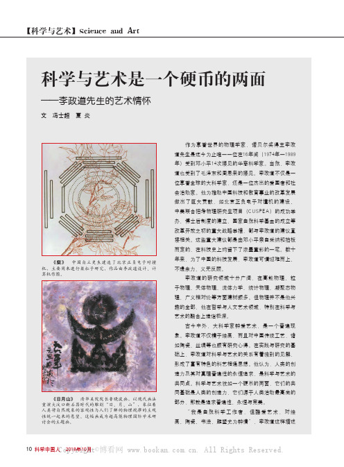
【科学与艺术】Science and Art《粲》 中国自立更生建造了北京正负电子对撞机,主要用来进行粲粒子研究,作品由李政道设计、计算机作图。
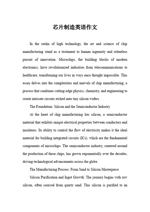
《日月山》 清华美院院长鲁晓波画,以现代画法重演大汶口新石器时代的雕刻“日、月、山”,象征着人类将自然现象的客观性与人们了解的物理规律的主观性统一起来的愿望。
这幅画成为超高能物理国际学术研讨会的主题画。
《无尽无极》 中央美院原院长吴作人画,已成为北京正负电子对撞机的标志。
《核子重如牛,对撞新生态》 李可染画,画中两牛角相峙似乎是完全静态的,但蕴含在画中的巨大能量是显而易见的。
李可染说,他一生所作的画都是和平的,这是他第一次描绘斗争和矛盾,以表现人类征服自然的决心。
《超弦生万象》 李可染画【科学与艺术】Science and Art《流光》 吴冠中画,李政道与吴冠中切磋后,用一首诗来解释《流光》:“点、线、面,黑、白、灰,红、黄、绿,最简单的因素,营造极复杂的绘画,它们结合在一起,光也不能留时间,流光—流光,流光容易把人抛,红了樱桃,绿了芭蕉。
”《大鹏》 清华大学首批文科资深教授、著名画家刘巨德从庄子《逍遥游》中得到启发,“北冥有鱼,其名为鲲……化而为鸟,其名为鹏;鹏之背,不知其几千里也;怒而飞,其翼若垂天之云……背负青天”,以展翅之白鹏象征宇宙,作为中国高等科学技术中心1998年“宇宙的过去与未来”国际学术研讨会主题画。
作者简介:冯士超 镇江市原副市长夏 炎 《科学中国人》副总编辑、首席记者《三维朱雀》 鲁晓波画《晓阳辐射新学光》 李可染画《创天》 中央工艺美院原院长、著名画家常沙娜教授以她擅长的敦煌飞天笔法,为中国高等科学技术中心物质探索国际学术研讨会作“创天”主题画,该画气势宏雅、寓意深刻,以“妙手托出星云展,艺境创天万物生”,来表现人类对物质和宇宙奥秘的探索。
《雷神引高能》 常沙娜画《雷神引高能》(二) 常沙娜画《格》 1987年5月中国高等科学技术中心成立后首次国际学术研讨会的主题图案(“格”字由李政道书写,含格物致知之意,其背景是并行计算机的线路图)。
芯片制造英语作文
芯片制造英语作文In the realm of high technology, the art and science of chip manufacturing stand as a testament to human ingenuity and relentless pursuit of innovation. Microchips, the building blocks of modern electronics, have revolutionized industries from telecommunications to healthcare, transforming our lives in ways once thought impossible. This essay delves into the complexities and marvels of chip manufacturing, a process that combines cutting-edge physics, chemistry, and engineering to create intricate circuits etched onto tiny silicon wafers.The Foundation: Silicon and the Semiconductor IndustryAt the heart of chip manufacturing lies silicon, a semiconductor material that exhibits unique electrical properties between conductors and insulators. Its ability to control the flow of electricity makes it the ideal material for building integrated circuits (ICs), which are the fundamental components of microchips. The semiconductor industry, centered around the production of these chips, has grown exponentially over the decades, driving technological advancements across the globe.The Manufacturing Process: From Sand to Silicon MasterpieceSilicon Purification and Ingot Growth: The journey begins with raw silicon, often sourced from quartz sand. This silicon is purified to anextraordinary degree, removing impurities to near-atomic perfection. The purified silicon is then melted and shaped into large cylindrical ingots, ready for slicing.Wafer Production: Using precision diamond blades, the ingots are sliced into thin wafers, each serving as the substrate for numerous microchips. These wafers undergo further cleaning and polishing to ensure a smooth, defect-free surface.Patterning and Lithography: The magic of chip manufacturing truly unfolds during the patterning process. Using complex lithography techniques, tiny patterns of circuits are projected onto the wafer's surface, covered with a photosensitive material called photoresist. The exposed areas are then etched away, leaving behind the intricate patterns that will form the basis of the chip's circuitry.Doping and Diffusion: To create transistors and other electronic components, specific regions of the wafer are doped with impurities, altering their conductivity. This process, known as doping, is followed by diffusion, where the dopants are distributed through the wafer to create the desired electrical properties.Layering and Interconnects: Multiple layers of materials are deposited on the wafer, each layer containing different components of the circuit. These layers are interconnected through tiny metal lines, forming the complex network that enables data transmission within the chip.Testing and Packaging: Before being packaged, each chip undergoes rigorous testing to ensure it functions correctly. Defective chips are discarded, while functioning ones are encapsulated in protective packages, ready for integration into electronic devices.The Future of Chip ManufacturingChip manufacturing continues to evolve at a breathtaking pace, driven by the relentless demand for faster, more efficient, and more powerful devices. Advancements in extreme ultraviolet (EUV) lithography, 3D integration, and nanoelectronics promise to push the boundaries of what is possible, enabling the creation of chips with unprecedented density and complexity.Moreover, the rise of artificial intelligence and machine learning is transforming the manufacturing process itself, optimizing production lines and reducing defects, further accelerating the pace of innovation.In conclusion, chip manufacturing is a symphony of technological prowess, blending the finest elements of physics, chemistry, and engineering to create marvels of microelectronics. As we continue to explore the frontiers of technology, the future of chip manufacturing holds limitless possibilities, promising to reshape our world in ways we can only begin to imagine.。
艺术与科学交汇英语作文
艺术与科学交汇英语作文Art and science are often viewed as two distinct disciplines, but in reality, they intersect and influence each other in profound ways. The combination of art and science can lead to innovative discoveries, creative expressions, and holistic understanding of the world.Firstly, art and science both involve creativity and imagination. Artists use their creativity to express emotions, ideas, and experiences, while scientists use their imagination to formulate hypotheses, design experiments, and solve complex problems. The synergy between artistic creativity and scientific imagination can spark new ideas and breakthrough innovations.Furthermore, art and science share a common goal of seeking truth and understanding the world around us. While artists may explore the human experience through visual, auditory, or performance mediums, scientists seek to uncover the laws of nature through observation, experimentation, and analysis. Both disciplines strive to deepen our knowledge and appreciation of the universe.Moreover, the collaboration between art and science can enhance communication and public engagement. Artisticrepresentations of scientific concepts can make complex ideas more accessible and engaging to a broader audience. Similarly, scientific advancements can inspire artistic creations that reflect the beauty and wonder of the natural world.In conclusion, the intersection of art and science is a rich and dynamic space where creativity, imagination, and exploration converge. By embracing the synergies between these disciplines, we can foster innovation, inspire curiosity, and cultivate a deeper appreciation for the interconnectedness of all forms of human expression.中文翻译:艺术和科学通常被视为两种不同的学科,但实际上它们在深刻的方式下交汇并相互影响。
艺术与科学思辨作文
艺术与科学思辨作文英文回答:Art and science are two distinct disciplines that share a common goal: the exploration of the human condition. Art seeks to express and interpret the world through the senses, while science aims to understand and explain the world through reason and experimentation. Both disciplines relyon creativity and imagination to generate new insights, and both can contribute to our understanding of ourselves and the world around us.One of the most important ways that art and science can interact is through the process of visualization. Artists can create images that help us to see the world in new ways, and scientists can use visualizations to represent complex data and concepts. For example, the artist David Hockneyhas created a series of paintings that explore the way that we see space and depth, and the scientist Albert Einstein used visualizations to develop his theory of relativity.Another way that art and science can interact isthrough the process of metaphor. Artists can use metaphorsto create new ways of thinking about the world, and scientists can use metaphors to help them to understand complex scientific concepts. For example, the artist Pablo Picasso used the metaphor of a bull to represent the powerof nature, and the scientist James Watson used the metaphor of a double helix to represent the structure of DNA.Art and science can also interact through the processof collaboration. Artists and scientists can work togetherto create new works of art that explore scientific concepts, or to develop new scientific tools and technologies. For example, the artist Olafur Eliasson has collaborated with scientists to create a series of installations that explore the effects of climate change, and the scientist Jane Goodall has collaborated with artists to create a series of paintings that depict the behavior of chimpanzees.The interaction between art and science has a long and rich history. In the Renaissance, artists such as Leonardoda Vinci and Michelangelo studied anatomy and natural history in order to create more realistic works of art. In the 19th century, scientists such as Charles Darwin and Alfred Russel Wallace used art to illustrate their theories of evolution. And in the 20th century, artists such as Marcel Duchamp and Salvador Dalí used scientific concepts to create new forms of art.Today, the interaction between art and science is more vibrant than ever. Artists and scientists from all over the world are collaborating to create new works of art that explore the most pressing issues of our time, such as climate change, artificial intelligence, and the future of humanity.中文回答:艺术与科学是两个截然不同的学科,但它们有同一个目标,探索人类境况。
《科学研究的艺术》由澳大利亚微生物学家、动物病理学家
《科学研究的艺术》由澳大利亚微生物学家、动物病理学家贝佛里奇撰写。
《科学研究的艺术》中文版第一版由科学出版社于1979年2月出版,目前由我社再版,曾荣登三联书店“20年来对中国影响最大的100本书”之列。
《科学研究的艺术》从科学研究的实践与思维技巧方面综合了一些著名科学家具有普遍意义的观点,分析了在科学上作出新发现的方法,总结了科学研究中有益而又有趣的经验教训,提出了可供各种学科参考的指导原则与思维技巧。
正如书中引言:“科学研究是一种艺术,不是科学。
——W•H•乔治”什么是科学研究的艺术?我想到这样一个传奇:一个多月以前,NASA的一位传奇科学家去世了,NASA专门发微信回顾了他的传奇经历,引起全世界网友的热议。
他叫Robert Farquhar,之前在美国NASA工作了几十年,参与了很多太空探测项目。
他最擅长的,就是卫星轨道的计算。
别人都说,他能把任何飞船送入人们想要送去的任何地方,他就是“轨道计算的大师”!1981年,NASA发射了一颗普通探测太阳粒子的卫星ISEE-3,这颗卫星被发射到了一个地球和太阳之间的某条轨道上,在这条轨道上,卫星受到的太阳和地球的引力相抵消,不用耗费什么燃料就可以在停留在地球和太阳之间相对静止的运行。
这是人类历史上第一颗被发送到这条“神奇轨道”的卫星,而算出这条轨道的人,就是Robert。
这个探测器在这个点上观察太阳观察了5年,卫星的使命也即将结束……然而,在那个时候,全世界的宇航科学家们都在做一件事情:哈雷彗星。
那时,这颗全世界最著名的彗星马上就要在1986年回归地球。
在那个太空竞赛的年代,俄罗斯,欧洲和日本都争相发射了彗星探测器,准备要在1986年探测哈雷彗星,这些彗星探测器提前几年就开始向哈雷彗星飞奔,史称——“哈雷舰队”。
但是,哈雷舰队里并没有美国的探测器。
美国表示,彗星任务太花钱,他们不准备去探索。
Robert却并不这样认为,他自己计算出了一个复杂的轨道,先让ISEE-3卫星返回地球,环绕N圈,利用月球的重力加速,去追赶彗星。
科技和非遗结合的英语作文
科技和非遗结合的英语作文非遗即非物质文化遗产。
以下是一篇关于科技和非遗结合的英语作文:In the modern era, technology and intangible cultural heritage are coming together in exciting and innovative ways. This combination not only preserves and showcases our cultural heritage but also brings it to new audiences and creates new opportunities for its transmission.One example of this is the use of digital technology in documenting and archiving intangible cultural heritage. With advanced digitization techniques, we can now capture and store delicate art forms, performances, and traditional knowledge in a way that ensures their long-term survival. This allows future generations to access and appreciate these valuable assets, even as they may face the threat of being lost over time.Another aspect of the intersection of technology and intangible cultural heritage is the use of social media and online platforms. These tools provide a global stage for showcasing and sharing cultural traditions. Artists, craftsmen, and cultural practitioners cannow reach a wider audience, transcending geographical boundaries. This increased visibility helps raise awareness about the significance of intangible cultural heritage and encourages its continuation.Moreover, technology can also play a role in educational initiatives related to intangible cultural heritage. Interactive apps, virtual reality experiences, and educational software can make learning about traditional practices more engaging and accessible. By making it easier for people to understand and connect with their cultural roots, we foster a greater appreciation for intangible cultural heritage.Furthermore, technology can facilitate the economic sustainability of intangible cultural heritage. E-commerce platforms and crowdfunding campaigns can provide new avenues for artists and artisans to sell their traditional products and gain financial support. This not only helps them continue their craft but also encourages the transmission of these skills to others.The integration of technology and intangible cultural heritage is a win-win situation. It allows us to safeguard and celebrate our cultural diversity while leveraging the power of technology to ensure its viability in the modern world. By combining the best of the past withthe advancements of the present, we can ensure that intangible cultural heritage remains an integral part of our collective identity and is passed on to future generations.这篇作文探讨了科技与非遗结合的几个方面,包括数字技术的应用、社交媒体和在线平台的作用、教育倡议以及经济可持续性。
俞书宏会变戏法的材料“魔术师”俞书
创新先锋|臨臟俞书宏:会变戏法的材料“魔术师”俞书宏院士(图/中国科学技术大学官网)近日,在北京举行的第二届全国创新争先奖表彰奖励大会上,中科院院士、中国科学技术大学教授俞书宏被授予全国创新争先奖章。
沉甸甸的奖章,展现了被誉为材料"魔术师”的俞书宏在无机仿生材料领域的卓越成就。
瞄准原始创新大自然就像是一个奇妙的“合成工厂”,不断制造出具有各种奇异功能的生物材料或生物体。
研究这些生物材料的结构和性能,能为人们在微尺度上的仿生材料设计开辟新的途径。
从事无机材料研究20余年以来,俞书宏不断地观察自然,获取仿生合成的灵感;又不断解密自然,追溯新型材料组装原理。
近年来,他率领团队建立了人工仿生合成珍珠母、人工木材、人工盔甲等多级结构材料的合成方法,阐释了其生长机理,发现了无机仿生材料跨尺度合成的新途径,在无机化学领域摘得累累硕果。
"这种新型天然纳米纤维素高性能仿生结构材料,具有优异的综合性能。
它的密度仅为钢的六分之一,而比强度和比韧性均超过传统合金材料、陶瓷及工程塑料,所以它有望替代现有的工程塑料,在航空、航天、军事、国防、民生等领域具有广泛的应用前景。
”不久前,俞书宏公布了团队的最新科研成果。
在他的实验室里,有制造这种新型材料的基础材料种白色果冻状半凝固体。
"它主要是利用天然纤维素制成,别看它相貌平平,却可以衍生制造出一系列致密又透气的材料产品。
比如,可以制作医用□罩的过滤层,有望用来替代熔喷布;可以制造轻巧耐用美观又防火的家具;可以制成飞行器部件、环保涂料、包装袋等。
”俞书宏介绍道,因为2020.8发明与创新21臨鸚昴1创臟锋俞书宏院士(左三)指导学生进行新材料研发(徐雯昊摄)在自然界中有大量可利用纤维素存在于灌木、秸秆等生物质中,所以原料成本更低,甚至可以变废为宝,一举两得。
俞书宏介绍,该材料的轻质高强韧性能主要来自材料微米级层状结构和纳米三维网络结构设计,纤维素纳米纤维内部高度结晶可以提供极高的强度,纤维之间通过大量氢键等可逆相互作用网络进行结合,在外力作用下这种高密度的可逆相互作用网络可以迅速解离和重构,吸收大量能量,使材料在具有高强度的同时实现高韧性,克服了传统结构材料难以兼具高强度与高韧性的问题。
介绍微雕技艺作文英语
介绍微雕技艺作文英语Title: The Art of Microcarving: A Delicate Craft。
Microcarving, a delicate art form originating from ancient cultures, has evolved into a sophisticated technique known as micro-engraving or micro-sculpting. This intricate artistry involves carving minuscule designs onto surfaces, often requiring specialized tools and a meticulous hand. In this essay, we delve into the realm of microcarving, exploring its history, techniques, and contemporary applications.Historical Roots:Microcarving finds its roots in ancient civilizations such as Egypt, Greece, and China. These cultures employed microcarving techniques to adorn jewelry, pottery, and architectural elements with intricate designs. In ancient China, artisans mastered the art of microcarving on materials like jade and ivory, creating exquisitesculptures and ornaments that are revered to this day.Techniques:Modern microcarving techniques have advanced significantly, owing to technological innovations and refined craftsmanship. Artisans utilize specialized tools such as microscopes, engraving needles, and lasers to achieve precision in their work. The process begins with selecting a suitable material, often gemstones like diamonds or rubies due to their hardness and clarity. The artisan then meticulously sketches the design before delicately carving it onto the surface of the material. The intricacy of microcarving requires immense patience and skill, as even the slightest error can ruin the entire piece.Challenges and Rewards:Microcarving presents a unique set of challenges compared to traditional carving methods. Working on such a small scale demands steady hands, acute vision, and anunderstanding of the material's properties. Moreover, the fragility of the medium means that one must exercise caution throughout the entire process to avoid accidental damage. However, the rewards of mastering microcarving are unparalleled. The ability to breathe life into minute details and create awe-inspiring pieces of art is immensely gratifying for artisans and viewers alike.Contemporary Applications:In the modern era, microcarving has found diverse applications across various industries. In the realm of jewelry, micro-engraving allows designers to adorn pieces with intricate motifs, adding a touch of elegance and sophistication. Beyond adornment, microcarving has also found utility in security features for banknotes and identification documents. Microscopically engraved patterns and images serve as anti-counterfeiting measures, enhancing the security and authenticity of valuable documents.Conclusion:In conclusion, microcarving stands as a testament to the ingenuity and skill of artisans throughout history. From its humble beginnings in ancient civilizations to its contemporary applications in technology and art, microcarving continues to captivate and inspire. As technology advances and artistic boundaries expand, the art of microcarving will undoubtedly evolve, pushing the limits of what is possible on a minuscule scale.。
- 1、下载文档前请自行甄别文档内容的完整性,平台不提供额外的编辑、内容补充、找答案等附加服务。
- 2、"仅部分预览"的文档,不可在线预览部分如存在完整性等问题,可反馈申请退款(可完整预览的文档不适用该条件!)。
- 3、如文档侵犯您的权益,请联系客服反馈,我们会尽快为您处理(人工客服工作时间:9:00-18:30)。
Asociación Argentina de Materiales Registro N°ISSN 1668-4788 ART AND SCIENCE OF MICRO-PATTERNINGF. MÜCKLICH, A. LASAGNI, Functional Materials, Saarland University, Building 22,7. Stock, P.O. Box 15 11 50, D-66041 Saarbrücken, GermanyAbstractThis article provides a general review of the various techniques of patterning which are essential to scientific progress in many areas of biology, physics, chemistry, and materials science. The patterning techniques include optical lithography, E-beam lithography, imprint lithography, replica molding, microcontact printing, laser writing, holographic patterning and direct laser interference patterning. We have briefly introduced each patterning technique demonstrating its potential and limitations. Some applications and examples are also introduced indicating the flexibility of the methods and the large spectra where these techniques can be applied that would be difficult or impossible to realize with conventional approaches.ARTE Y CIENCIA DE LA MICRO-IMPRESIÓNResumenEste artículo provee una revisión general de distintas técnicas de micro impresión las cuales son esenciales para el progreso científico en áreas de biologia, física, química y ciencia de materiales. Las técnicas de micro impresión incluyen litografía óptica, litografía electrónica, litografía por impresión, réplica por medio de moldes, impresión por microcontacto, micro impresión holográfico y micro impresión directa por interferencia laser. Cada uno de estos métodos ha sido brevemente introducidos demostrando su potencialidad y limitaciones. Algunas aplicaciones y ejemplos son tambien descriptos indicando la flexibilidad de estos métodos y el gran espectro donde pueden ser aplicados, lo cual sería muy difícil o prácticamente imposible de realizar utilizando métodos convencionales.Asociación Argentina de Materiales Registro N°ISSN 1668-4788 ART AND SCIENCE OF MICRO-PATTERNINGF. MÜCKLICH, A. LASAGNI, Functional Materials, Saarland University, Building 22,7. Stock, P.O. Box 15 11 50, D-66041 Saarbrücken, Germany1- IntroductionNew methods for micro- and nanofabrication are essential to scientific progress in many areas of biology, physics, chemistry, and materials science. They also form enabling technologies for applications ranging from microfluidic devices to micro-optical components to molecular diagnostics to plastic electronics to nanoelectromechanical systems. In many cases, these advances are aided by the highly engineered and spectacularly successful lithographic techniques that are used for microelectronics [1].Patterning techniques can be divided a priory into two large groups: (1) methods which require mechanical processes to produce the patterning, and (2) methods which are activated by light, electrons or ions.The first group includes techniques based on printing, molding and embossing. These techniques represent new conceptual approaches to the fabrication and manufacturing of new types of structures and devices on planar, curved or flexible substrates. It also appears to be a promising route to structures and systems for emerging applications in biotechnology [2].The second large group includes optical lithography, E-Beam lithography, laser writing, holographic patterning and direct laser interference patterning, amongst others.Many of the basic principles of these methods are, of course, conceptually not new; embossed gold coins were first produced around 600 BC, and the printing press was invented in the 15th century. Nevertheless, recent research proves that these ideas, and variants of them, can be dramatically improved and extended into the nanometer range by introducing advanced materials, chemistries, and processing techniques. The resulting methods possess truly remarkable patterning capabilities.The process of patterning is also commonly referred to as lithography, which involves a flow of information that typically begins with the design of a pattern in the form of a dataset and ends at a patterned array of features on the surface of a substrate [3]. There can be many steps in between, and each one of these steps may impose the possibility of losing information or pattern distortion. In general, a lithographic technique is built upon following key elements:a) a pre-designed set of patterns in the form of a mask or a masterb) a means to mediate the transfer or replication patternsc) a responsive medium, which is usually a functional material capable of serving asthe resist for subsequent stepsd) and tools that ensure appropriated metrologyAsociación Argentina de Materiales Registro N°ISSN 1668-4788Depending on the application, the requirements for a successful lithographic process can vary substantially. The critical feature size of the test patterns is probably the most obvious issue one must consider when selecting a proper lithographic technique.This article intends to provide a general review of the various techniques of patterning. Several of the topics presented here demonstrate the power of these new lithographic techniques, through their application to functional prototype systems that would be difficult or impossible to realize with conventional approaches.2- Patterning techniques2.1- Optical LithographyThe name optical lithography comes from the early application where the exposing energy was visible light. While those wavelengths can still be used, the push to reduce the size of feature sizes has lead to the use of shorter wavelengths to increase resolution. Ultraviolet (UV) and deep ultraviolet (DUV) sources are also now employed. Such sources include excimer lasers which operate at wavelengths of 248 nm, 193 nm, and less. Visible wavelengths end in the red at about 400 nm. At these shorter wavelengths, particularly 193 nm, optical materials and even air absorb the energy very well [4].In optical lithography, printing is the process of projecting the image of the patterns onto the substrate surface using a light source and a photo mask.Patterned masks, usually composed of glass or chromium, are used during printing to cover areas of the photoresist layer that shouldn't get exposed to light. Development of the photoresist in a developer solution after its exposure to light produces a resist pattern on the substrate, which defines which areas of the substrate are exposed for material deposition or removal (Fig. 1).There are two types of photoresist material, namely, negative and positive photoresist. Negative resists are those that become less soluble in the developer solution when exposed to light, forming negative images of the mask patterns on the wafer. On the other hand, positive resists are those that become more soluble in the developer when exposed to light, forming positive images of the mask patterns on the substrate.Commercial negative photoresists normally consist of two parts: 1) a chemically inert polyisoprene rubber; and 2) a photoactive agent. When exposed to light, the photoactive agent reacts with the rubber, promoting cross-linking between the rubber molecules that make them less soluble in the developer. Such cross-linking is inhibited by oxygen, so this light exposure process is usually done in a nitrogen atmosphere.Positive resists also have two major components: 1) a resin; and 2) a photoactive compound dissolved in a solvent. The photoactive compound in its initial state is an inhibitor of dissolution. Once this photoactive dissolution inhibitor is destroyed by light, however, the resin becomes soluble in the developer. A disadvantage of negative resists is the fact that their exposed portions swell as their unexposed areas are dissolved by theAsociación Argentina de Materiales Registro N°ISSN 1668-4788developer. This swelling, which is simply volume increase due to the penetration of the developer solution into the resist material, results in distortions in the pattern features.Figure 1. Process of optical lithography. Theprojection optical system is used to exposethe resist film to light in the shape of desiredpatterns. This exposure creates a chemicalchange in the resist film which depending onthe tone of the resist makes the exposedresist region more or less soluble in adeveloping solvent. The resist film isdeveloped to produce desired protectiverelief pattern. The resist pattern is used insubsequent processes such as etching, andresist film is finally removed.Since optical lithography works so well (producing 180nm features in modern Intel fabs), the question becomes: "Why not simply use masks with ever smaller features?" Obviously smaller mask features translates to smaller surface features. While this is true, there is another limitation to any optical system: the wavelength of light used. The resolution of any optical system (be it a microscopy or lithographic system) is limited both by configuration and the wavelength of light [5, 6]:NA k R λ= (1)where the resolution R , is defined by configuration features (k is usually on the order of 1) and NA, the numerical aperture, on the order of 1.6, and λ the wavelength of light.This effect is called the diffraction limit. Diffraction is an inevitable consequence of the wave nature of light, and is responsible for the spreading of light as it passes through, for example, a slit cut into a screen. This means that feature sizes can typically only be made on the order of the wavelength of light used. At best, features at half the wavelength of light can be created, but no smaller.2.2- E-Beam LithographyFor lateral structuring below the resolution limit of photolithography (< 200 nm), e-beam lithography is by far the widest spread lithography tool. Compared to other nanostructuring methods, it combines high resolution with excellent flexibility and reasonable patterning speed.The setup of e-beam Lithography is similar to a Scanning Electron Microscope and often a scanning electron microscope is used. The dissipation of beam energy can proceed in a number of different ways and may include various types of physical and chemical processes, depending on the type of radiation, its dose, and the materials that are involved. Generally, the patterning process can be additive, involving the deposition of species in or close to the illuminated spot, or subtractive due to the removal of material from the surface of a substrate [7].Asociación Argentina de Materiales Registro N°ISSN 1668-4788 The scan rate is adjusted to deliver a critical dose of electrons to a selected area of the resist. Any structure desired can be created as a CAD file and written directly using suitable control software. Thus this method is ideally suited for developing prototypes and no masks are required.Figure 2. (a) Schema of a focused electron-beam inducing changes in a resist material. (b)A bragg-Fresnel lens for x-rays exposed in continuous path control mode and etched into Si[8].The resist is either developed in a chemical bath similar to photolithography, or the electron beam interacts with the material sufficiently to remove the resist material (Fig. 2). The result from exposing a resist is that the molecular linear chain is broken and the average molecular weight of the polymer exposed area is reduced. Reducing the molecular weight of the polymer is accompanied by an increase of the solubility, and therefore in the etching rate. Thus, the principal result from exposure is a pattern drawn in terms of etching rate.2.3- Imprint LithographyImprint lithography involves two steps: imprinting and pattern-transfer (Fig. 3). In the imprinting step, a mold with nanostructures on its surface is used to deform a thin resist film or an active material deposited on a substrate. In the pattern-transfer step, an anisotropic etching process such as reactive ion-etching is used to remove the residual resist in the compressed area, transferring the thickness-contrast pattern created by the imprint into the entire resist [9, 10].The polymer must be either thermoplastic, UV- or thermically curable, or otherwise deformable to adapt the shape of the patterns on the master. In the case of thermoplastic materials, the substrate must be heated above its glass-transition temperature (T g) during imprinting, and then cooled below T g. before it is separated from the master. When the polymer is a UV- or thermally curable material, it is imprinted in its liquid state, and then hardened into patterned structures through a UV- or thermal-curing process. In most cases, residual films of the polymer remain in the compressed areas, which can be removed using a dry etching process.Asociación Argentina de Materiales Registro N°ISSN 1668-4788Figure 3. Schematic illustration of theimprint lithography process:(a) Imprinting, using a mold to create athickness contrast in a resist.(b) Pattern-transfer, using anisotropicetching (reactive ion etching) to removeresidue resist in the compressed areas.Imprint lithography is primarily a physical-deformation process and is fundamentally different from other lithographic methods such as “stamping” with self-assembling “ink” [12]. Its simple yet unique principle allows this method to avoid many problems inherent in other lithographic methods and to achieve high resolution and high throughput at a low cost. The resolution of imprint lithography is determined by the mechanical strength of the mold and polymer.Figure 4. SEM micrograph of a perspectiveview of strips formed into a PMMA film byimprint. The strips are 70 nm wide and 200nm tall, have a high aspect ratio, a surfaceroughness less than 3 nm, and nearlyperfect 90° corners [11].Imprint lithography can be carried out using three different types of imprinting machines: single-imprint, step-and-repeat, and roller. The single-imprint machine imprints an entire wafer at one time (Fig. 3). The step-and-repeat machine imprints a small area (called a die) of a wafer at a time and then moves to a new area of the wafer. The process is repeated until the entire wafer is imprinted. One advantage of the step-and-repeat method is that it is easier to achieve higher alignment accuracy in a smaller area than in a larger area. A second advantage, and probably the most significant for many applications, is that it allows the use of a very small mold to create a large imprint area or a large imprintAsociación Argentina de Materiales Registro N°ISSN 1668-4788 mold. It takes several days of current electron-beam lithography to expose 10 nm features over the entire area of a 1 cm x 1 cm mold. Using step-and-repeat imprint lithography, the 1 cm x 1 cm mold can be used to pattern a much larger mold (e.g., an 8 in. diameter mold) in just few minutes. Fig. 4 shows 70 nm lines fabricated on a PMMA resist.Figure 5. Two ways for roller nanoimprint:(a) imprints using a cylinder mold: bending acompact master disk into cylinder shape,mounting it around the roller, and rolling theroller on the substrate; (b) imprints using aflat mold: putting the mold directly on thesubstrate, and rotating the roller on top ofthe mold [13].Roller-nanoimprinting machines have the advantage of better uniformity, less imprint force, simple construction, and the ability to use a mask continuously on a large substrate [13]. There are two ways to use Roller-nanoimprinting (Fig. 5). One uses a cylindrical mold, which can be made by bending a thin metal mold around a smooth roller. The other uses a smooth roller over a flat mold. To keep the shape of previously imprinted patterns while imprinting other areas, the substrate is held at a temperature below T g of the resist, but above T g of the mold.2.4- Replica MoldingReplica molding duplicates the information–for example, the shape, the morphology, and the structure–present in a master (see Fig. 6). It is a procedure that accommodates a wider range of materials than does photolithography. It also allows duplication of three-dimensional topologies in a single step, whereas photolithography is not able to replicate such structures. It has been used for the mass production of surface relief structures such as diffraction gratings, holograms, compact disks (CDs), and microtools. Replica molding with an appropriate material (usually in the form of a precursor) enables highly complex structures in the master to be faithfully duplicated into multiple copies with nanometer resolution in a reliable, simple, and inexpensive way [14, 15]The fidelity of replica molding is determined by Van der Waals interactions, wetting, and kinetic factors such as filling of the mold. These physical interactions should allow more accurate replication of features that are smaller than 100 nm than does photolithography, which is limited by optical diffraction.Asociación Argentina de Materiales Registro N°ISSN 1668-4788 The procedure for replica molding of [16] differs from conventional procedures in the use of an elastomeric mold rather than a rigid mold. The elasticity and low surface energy of the elastomeric mold allows it to be released easily. An elastomeric mold also offers the opportunity to manipulate the size and shape of features present on the mold by mechanical deformation. The capability and versatility of this new procedure has been demonstrated for nanomanufacturing. Conventional highresolution nanolithographic techniques are used to make masters, and these structures are then duplicated into multiple copies by replica molding with organic polymers. This technique has also been adapted for the fabrication of topologically complex, optically functional surfaces that would be difficult to fabricate with other techniques.Replica molding against elastomeric molds is possible with a resolution on the nanometer scale. For example, in Fig. 6.b AFM images of chromium structures on a master and a PU replica prepared from a poly(dimethylsiloxane) mold cast against this master are shown. The most important feature of this replicated polyurethane is the accuracy with which the vertical dimension is reproduced. The heights of the chromium lines on the original master were about 13 nm; the heights of the polyurethane lines were about 8 nm. The prepolymer of polyurethane used here shrinks less than 3% upon curing. These images demonstrate that this replica molding procedure duplicated structures within a few nanometers over substantial areas (ca. 1 mm2).Figure 6. (a) Schematicillustration of procedures forreplica molding; REM: Re-plica molding, PDMS: poly(dimethylsiloxane).(b) AFM images of chro-mium structures on a masterand a PU (polyurethane) re-plica prepared from a PDMSmold cast from this mas-ter.[16] The width is given inmicrometers; the depth andheight are given innanometers. [14]2.5- Microcontact printingMicrocontact printing is a flexible, non-photolithographic method that routinely forms patterned self-assembled monolayers (SAMs) containing regions terminated by different chemical functionalities with submicron lateral dimensions.Asociación Argentina de Materiales Registro N°ISSN 1668-4788 This technique uses a silicone stamp to deposit molecules on surfaces. The stamp is first 'inked' with a solution of molecules, often proteins or thiols which then either coat the stamp or, in the case of small molecules, are absorbed into the silicone in the form of a solid solution. The stamp is dried and pressed onto the surface to be patterned (see Fig.7).The soft silicone stamp makes conformal contact with the surface and molecules are transferred directly from the stamp to the surface in the space of a few seconds. After that, a different SAM can be formed on the underivatized regions by washing the patterned substrate with a dilute solution containing the second molecule.Figure 7. Schematic illustration of procedures for Microcontact printing of hexadecanethiol (HDT) on a gold surface: (a) printing on a planar surface with a planar stamp (I: printing ofthe SAM, II: etching, III: deposition) (b) large-area printing on a planar surface with a rolling stamp, (c) printing on a nonplanar surface with a planar stamp. After the ™ink (ca. 2 mmHDT in ethanol) was applied to the PDMS stamp with a cotton swab, the stamp was dried ina stream of N2 (ca. 1 min) and then brought into contact with the gold surface (ca. 10 ± 20 s)[14].Some examples of test patterns in silver that were fabricated using microcontact printing with hexadecanethiol, followed by wet chemical etching are presented in Fig. 8.Figure 8. SEM images of test patterns of silver (a–c, 50 nm thick; d, 200 nm thick) that were fabricated using microcontact printing with hexadecanethiol, followed by wet chemical etching. The patterns in (a) and (b) were printed with rolling stamps (see Fig.7b); the patterns in (c–d) were printed with planar stamps (see Fig.7.a). The bright regions are metals; the dark regions are Si/SiO2 exposed where the etchant has removed the unprotected metals [15].Asociación Argentina de Materiales Registro N°ISSN 1668-4788 The stamps for microcontact printing are normally made using micromachined silicon wafers. The wafers form part of a mould in which liquid silicone is polymerized. On demoulding, a flexible transparent stamp is obtained, with structures that can be as smallas 100nm.2.6- Laser writingWriting based on two-photon absorption has emerged as an attractive and versatiletool for generating 3D structures in various polymeric resists [17].Two-photon excitation provides a means of activating chemical or physical processes with high spatial resolutionin three dimensions and has made possible the development of three-dimensional fluorescence imaging, optical data storage and lithographic microfabrication. These applications take advantage of the fact that the two-photon absorption probability depends quadratically on intensity, so under tight-focusing conditions, the absorption is confined atthe focus to a volume of order λ3 (where λ is the laser wavelength). Any subsequent process, such as fluorescence or a photo induced chemical reaction, is also localized inthis small volume.In this technique, photo-polymerization occurs only in the vicinity of the focal point ofa laser beam thus generating a voxel, which is a 3D volume element of solidified resist.The patterning procedure is performed by pinpoint-scanning a focused laser according to apre-programmed pattern design in the form of a voxel matrix. The dimensions of such voxel are mainly determined by the spot size and pulse energy of the laser beam, and cango beyond the limitation of Rayleight diffraction.Figure 9.Three-dimensionalmicrostructures produced bytwo-photoninitiated poly-merization.(a) Photonic band-gapstructure. (b), Magnified top-view of structure in (a). (c)Tapered waveguidestructure. (d) Array ofcantilevers. The films wereexposed to Ti: sapphire laserpulses (150fs, 76MHz, at awave-length near the two-photon absorption peak ofthe initiator [17].To illustrate an example of the utility of laser writing, let’s consider the fabrication of potentially interesting 3D structures in a photopolymer system. Three-dimensional periodic structures are needed for photonic bandgap (PBG) materials, which have unique optical properties. These structures are difficult to fabricate on micrometre or submicrometre length scales as needed for applications in the infrared and visible spectral regions. Fig.9.a and b shows views of a “stack-of-logs” structure which, given a sufficiently highAsociación Argentina de Materiales Registro N°ISSN 1668-4788refractive index, should exhibit PBG properties in the infrared spectral region. High-refractive-index structures, based for example on refractory ceramics, could be fabricated by using the polymer structure as a preform. Other structures of arbitrary pattern and periodicity down to ~1 µm length scales could be readily obtained with this photopolymer system. Two-photon 3D laser writing could also find application in the production of tapered optical waveguides, such as those shown in Fig. 9.c. For the example shown, the waveguide cross-section varies along the length from a 100µm x 100 µm square aperture to a 2 µm x 10 µm rectangular aperture. Tapered optical waveguides have the potential to reduce optical loss in the coupling of waveguide components with disparate cross-sections. Microelectromechanical systems (MEMS) are often produced using two-dimensional lithography, and 3D structures are built up by an iteration of processing steps. As an example of MEMS structures easily fabricated with a single development step, we produced the array of polymeric cantilevers is shown in Fig. 9.d.2.7- Holographic patterningHolographic patterning involves the interference of two or more laser beams and allows rapid fabrication (~seconds) and high design flexibility not limited by multi-phase equilibrium [18]. The major advantage of this technique is that it is a relatively simple and fast process which consists on two steps: exposure and development.The interference patterns can be predicted in advance by calculation as follows [19]. Under the assumption of plane waves, the total electric field (E ) of the interference pattern can be obtained by the superposition of each individual “i” beam:()∑∑=−−===n i y x ik i n i i i i i e E E E 1sin cos sin 01ββα(2)where E i0 is the amplitude of the electric field of the i -beam; αi is the angle between the beam direction and the vertical direction perpendicular to the interference plane; βi is the angle between the projection of the beam on to the interference plane and the x -direction; and k is the wave-number:λπ2=k (3)where λ denotes the wave length of the beam.The intensity of the overlapped beams is proportional to the module of the total electric field distribution:2E I α (4)In the case of two coherent interfering laser beams an array of parallel lines will be created, in which the spacing between the lines is:Asociación Argentina de Materiales Registro N°ISSN 1668-4788()2/sin 2θλ=d (5)where θ is the angle in between the laser beams. This technique is widely used in the photonic industry to manufacture holographic diffractions gratings and anti-reflection coatings [20].More complex pattern can be formed by intersecting more than two laser beams or by using multiple sequential exposures. For example, when four coherent laser beams are focused onto the same spot, a 3D periodic lattice will be generated after the exposed regions have been removed by selective dissolution [21,22]. For example, if the configuration shown in Fig. 10.a of four wave vectors is employed, the 3D interference pattern shown in Fig. 10.b is obtained.Figure 10. (a) Appearance of four wave vectors that create b.c.c. inference fringe pattern. The four beams are symmetrically arranged. (b) Three-dimensional display of the light intensity distribution for the arrangement shown in Fig.10.a. Only parts that have intensity greater than the 50%of the maximum value are displayed. The length of each edge is 1.4 µm. [21]A particularly interesting application of this technique is the fabrication of 3D photonic crystals [22]. Multiple interference between waves scattered from each unit cell of the structure may open a “photonic bandgap”; a range of frequencies, analogous to the electronic bandgap of a semiconductor, within which no propagating electromagnetic modes exist. Numerous device principles that exploit this property have been identified. Considerable progress has been made in constructing two and three-dimensional structures using conventional lithography. In the case of three-dimensional holographic lithography, the production of three-dimensional structures with sub-micrometre periodicity was carried out by [22]. With this technique they have made microperiodic polymeric structures, and complementary structures have been produced by using these polymers as templates.The 3D-periodic microstructure is generated by interference of four noncoplanar laser beams in a film of photoresist typically 30 µm thick. The intensity distribution in the interference pattern has three-dimensional translational symmetry; its primitive reciprocal。