TDF8771A中文资料
NTS-700系列微机保护测控装置用户手册111103

目录
1 概述................................................................................................................................................................... 1
注意!
a) 装置应运行于其规定的电气和环境限值之内; b) 装置上电前,应明确连线与正确示图相一致; c) 装置上电使用前请仔细阅读说明书,参照说明书对装置进行操作、定值/运行参数整定和测试。如有
随机资料,相关部分以资料为准; d) 装置的“系统设置”和“保护定值”同样重要,应准确设定才能保证装置保护以外功能的正常运行; e) 改变当前保护定值将不可避免地要改变装置的运行,在作改变前应谨慎,并按规程作校验。
及离线配置。不经恰当接地操作装置,可能会损坏装置,也可能会发生事故引起伤害; e) 在正常运行期间,严禁断开或连接与端子相连的导线或连接件,可能会有致命的危险电压、电流,
也可能会中断设备的运行,损坏端子及测量电路; f) 严禁不短接电流互感器的二次绕组就断开其二次回路的连接。运行的电流互感器在二次绕组开路时,
NTS-700 系列微机保护测控装置
用户手册
V1.00
南京天溯自动化控制系统有限公司 2011 年 09 月
说明
1. 说明
本说明与相关的装置文件构成了安全操作、调试与测试的完整信息。在对装置作任何操作之前,使 用人员必须熟悉本说明的内容和装置铭牌的额定参数。
2. 健康和安全
装置的正常和安全运行,依赖于恰当的运输、搬运和正确的贮存、安装和调试,以及细心的操作、 维护和维修。因此,只有合格人员才可操作或在装置上工作。合格人员是指:
LP8773 第二代准谐振 PWM 控制器 说明书
概述LP8773是一款高性能的第二代准谐振PWM隔离反激控制器。
内置专有的准谐振技术以及高可靠的保护功能。
LP8773的“数字抗抖动”技术可以根据加载自动选择和锁定波谷,可以实现无音频噪声操作。
另外,“数字抖频”功能使LP8773与传统的QR相比,EMI 性能更优。
LP8773具有多模式控制方式。
满载时,根据输入电压不同,芯片工作于CCM模式或QR模式。
当负载减轻,芯片进入“数字频率监控”模式来提高功率转换效率。
当输出功率非常小时,芯片进入突发模式,可以达到100mW以下的待机功耗。
LP8773集成多种保护功能,包括欠压保护、VCC 过压保护、输出过压保护、逐周期电流限、管脚浮空保护、过载保护、输入电压断电保护、软启动、VCC钳位、Gate钳位等。
LP8773的保护功能都可以自适应恢复。
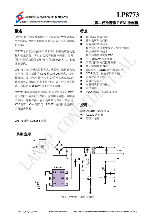
LP8773采用SOT23-6封装特点⏹轻松满足能效六级⏹输入电压断电保护⏹专有的准谐振技术数字抗抖动技术实现无音频噪声操作数字频率监控技术数字抖频技术优化EMI⏹小于100mW待机功耗⏹多模式控制方式提升效率⏹最大限制频率80KHz⏹QR模式,52KHz最小频率限制⏹CCM模式,自适应斜坡补偿⏹内置软启动功能⏹管脚浮空保护⏹内置同步斜坡补偿⏹前沿消隐⏹VDD欠压、过压以及钳位应用隔离AC/DC反激变换器⏹AC/DC适配器⏹SMPS电源图1 LP8773 典型应用图定购信息极限参数(注1)注1:保证满足个别性能指标。
电气参数定义了器件在工作范围内并且在保证特定性能指标的测试条件下的直流和交流电参数规范。
对于未给定上下限值的参数,该规范不予保证其精度,但其典型值合理反映了器件性能。
注2:芯片不保证参数以外的操作条件典型特性曲线电气参数(无特别说明情况下,VDD=15 V,T=25℃)A内部结构框图图3 LP8773内部框图.应用信息LP8773是一款高性能的第二代准谐振PWM隔离反激控制芯片。
内置专有的准谐振技术以及高可靠的保护功能。
PIC16f877中文资料1
PIC16F877原理简介1.1 PIC16F877特性:PIC16F877是由Microchip公司所生产开发的新产品,属于PICmicro系列单片微机,具有Flash program程序内存功能,可以重复烧录程序,适合教学、开发新产品等用途;而其内建ICD(In Circuit Debug)功能,可以让使用者直接在单片机电路或产品上,进行如暂停微处理器执行、观看缓存器内容等,让使用者能快速地进行程序除错与开发。
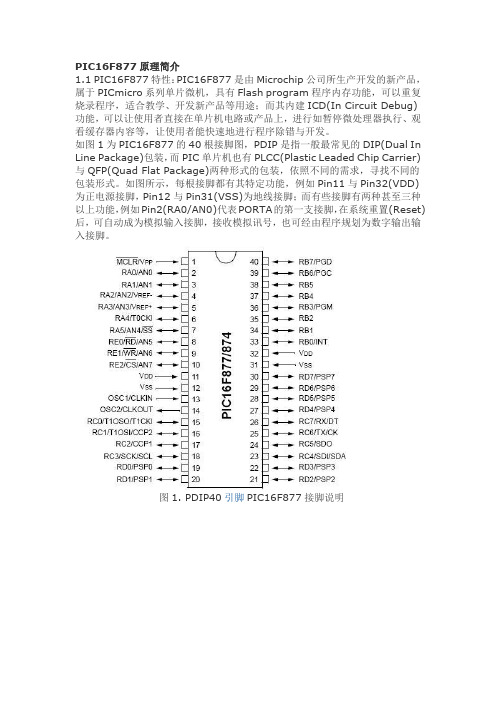
如图1为PIC16F877的40根接脚图,PDIP是指一般最常见的DIP(Dual In Line Package)包装,而PIC单片机也有PLCC(Plastic Leaded Chip Carrier)与QFP(Quad Flat Package)两种形式的包装,依照不同的需求,寻找不同的包装形式。
如图所示,每根接脚都有其特定功能,例如Pin11与Pin32(VDD)为正电源接脚,Pin12与Pin31(VSS)为地线接脚;而有些接脚有两种甚至三种以上功能,例如Pin2(RA0/AN0)代表PORTA的第一支接脚,在系统重置(Reset)后,可自动成为模拟输入接脚,接收模拟讯号,也可经由程序规划为数字输出输入接脚。
图1. PDIP40引脚PIC16F877接脚说明图2. PDIP28和SOIC28引脚PIC16F877接脚图说明图3. PLCC44引脚PIC16F877脚位图说明图4. QFP44引脚PIC16F877引脚图说明PIC16F877属于闪控式(Flash)单片机,可以重复烧录,其ROM的容量总共是8K words,以2K为一个page,区分为4个pages;内部RAM总共有512个字节(00f~1FFh),以128个字节为一个Bank,共区分为4个Bank,如图5所示,每个Bank的前半段都有其特殊用途,分别连接到其特殊功能模块,例如I/O、CCP、Timer、USART、MSSP等。
tc787各引脚参数 Microsoft Word 文档

三相可控硅移相触发电路TC787(AP)TC787(AP)是采用先进IC工艺设计制作的单片集成电路,可单电源工作,亦可双电源工作,主要适用于三相可控硅移相触发电路和三相三极管脉宽调制电路,以构成多种调压调速和变流装置。
该电路作为TCA785的换代产品,与目前国内市场上流行的KC系列电路相比,具有功耗小、功能强、输入阻抗高、抗干扰性能好、移相范围宽,外接元件少等优点;而且装调简便,使用可靠。
只需要一块这样的集成电路,就可以完成三块TCA785或五块KC系列器件组合(三块KC009或KC004,一块KC041,一块KC042)才能具有的三相移相功能。
因此TC787, TC788可广泛应用于三相全控,三相半控,三相过零等电力电子,机电小型化产品的移相触发系统,从而取代TCA785、KC009、KC004、KC042、KC042等同类电路,为提高整机寿命,缩小体积,降低成本提供了一种新的更加有效的途径。
一. 特点:▪电路采用单电源工作,电源电压8V~15V。
▪三相触发脉冲调相角可在0~180°之间连续同步改变。
▪识别零点可靠,可方便地用作过零开关。
▪器件内部设计有交相锁定电路,抗干扰能力强。
▪可用于三相全控触发(6脚接VDD),也可用于三相半控触发(6脚接地)。
▪电路备有输出保护禁止端,可在过流过压时保护系统安全。
▪TC787输出为调制脉冲列,适用于触发可控硅及感性负载。
▪调制脉冲或方波的宽度可根据需要通过改变电容Cx而选择。
二. 电路原理和逻辑框图:▪电路组成:由三路相同的部分:同步过零和极性检测、锯齿波形成、锯齿波比较,经过抗干扰锁定、脉冲形成等电路形成三相触发调制脉冲或方波,由脉冲分配电路实现全控、半控的工作方式,再由驱动电路完成输出驱动。
▪电路原理:三相同步电压经过T型网络进入电路,同步电压的零点设计为1/2电源电压(电路输入端同步电压峰峰值不宜大于电源电压),通过过零检测和极性判别电路检测出零点和极性后,在Ca、Cb、Cc三个电容上积分形成锯齿波。
XPT4871用户手册
XPT4871 用户手册XPT4871 用户手册2006 年 7 月版权所有,侵权必究深圳市矽普特科技有限公司 第 1 页 ,共 18 页XPT4871 用户手册 目 录1 芯片功能说明 ···························································································································4 1.1 1.2 1.3 1.4 1.4.1 1.4.2 2 芯片主要功能特性·································································································4 芯片应用场合·········································································································4 芯片基本结构描述·································································································4 芯片的封装和引脚·································································································5 SOP封装 ·················································································································5 XPT4871 管脚描述 ································································································5芯片特性说明 ···························································································································5 2.1 2.2 2.3 2.4 2.4.1 2.4.2 2.4.3 2.4.4 2.4.5 芯片最大极限值·····································································································5 芯片数字逻辑特性·································································································6 芯片性能指标特性·································································································6 XPT4871 的典型参考特性·····················································································7 总谐波失真(THD),失真+噪声(THD+N),信噪比(S/N) ···················7 电源电压抑制比(PSRR) ·················································································10 芯片功耗(Power Dissipation)··········································································11 关断滞回(Shut Down Hysteresis)····································································11 输出功率(Output Power) ······················································································123XPT4871 应用说明 ················································································································13 3.1 3.2 3.3 3.4 3.5 3.6 3.7 3.7.1 3.8 外部电阻配置·······································································································13 芯片功耗 ··············································································································13 电源旁路 ··············································································································14 掉电模式 ··············································································································14 外围元件的选择···································································································14 选择输入耦合电容·······························································································14 设计参考实例·······································································································14 设计规格 ··············································································································14 其它注意事项·······································································································154 5芯片的封装·····························································································································16 XPT4871 典型应用电路 ········································································································18版权所有,侵权必究深圳市矽普特科技有限公司 第 2 页 ,共 18 页XPT4871 用户手册图目录图 1 XPT4871 原理框图 ········································································································4 图 2 大增益模式工作电路结构···························································································15 图 3 MSOP封装尺寸图········································································································16 图 4 SOP封装尺寸图 ···········································································································16 图 5 LLP封装尺寸图 ···········································································································17 图 6 DIP 封装尺寸图 ···········································································································17 图 7 XPT4871 典型应用电路 ······························································································18 图 8 XPT4871 两声道叠加应用电路···················································································18表目录表 1 XPT4871 管脚描述(SOP封装) ...................................................................................5 表 2 芯片最大物理极限值.......................................................................................................5 表 3 关断信号数字逻辑特性...................................................................................................6 表 4 芯片性能指标 1(VDD=5.0V,TA=25oC) .................................................................6版权所有,侵权必究深圳市矽普特科技有限公司 第 3 页 ,共 18 页XPT4871 用户手册 芯片功能说明XPT4871 是一款桥式音频功率放大器。
tSH-700 系列繁體中文使用手冊说明书

tSH-700系列繁體中文使用手冊精簡型序列埠分享器 2020年6月 版本: 1.8:目錄檢查配件 (4)更多資訊 (4)1.產品介紹 (5)1.1選型指南 (7)1.2規格 (8)1.3配置圖 (9)1.4機構圖 (11)1.4.1tSH-700 系列模組 (11)1.4.2CA-002 DC 電源線 (12)1.5腳位定義 (13)2.啟動 TSH-700 模組 (14)步驟1:連接電源和電腦主機 (14)步驟2:連接M ASTER和S LAVE設備 (16)步驟3:安裝軟體到您的電腦 (17)步驟4:配置正確的網路設定 (17)步驟5:配置A PPLICATION M ODE (19)步驟6:配置序列埠設定 (20)步驟7:測試您的T SH-700模組 (21)3.配置網頁 (23)3.1登入 T SH-700網頁伺服器 (23)3.2H OME首頁 (25)3.3A PPLICATION M ODE (26)3.3.1Converter Application (tSH-72x 系列) (26)3.3.2Sharer Application (tSH-73x 系列) (29)3.4S ERIAL P ORT 配置 (32)3.4.1Port1 Settings (32)3.5N ETWORK S ETTING配置頁 (34)3.5.1IP Address Settings (34)3.5.2General Settings (36)3.5.3Restore Factory Defaults (38)3.5.4Firmware Update (40)3.6F ILTER配置頁 (41)3.6.1 Accessible IP (filter is disabled when all zero) .......................................................................................... 41 3.7 M ONITOR 配置頁 .............................................................................................................................................. 42 3.8 C HANGE P ASSWORD 配置頁 ............................................................................................................................... 43 3.9L OGOUT 配置頁 (43)附錄 A: 疑難排解 ....................................................................................................................................................... 44 如何恢復模組原廠預設的網頁伺服器登入密碼? ...................................................................................................... 44 附錄 B: 應用注意 ....................................................................................................................................................... 46 如何設定 T IMEOUT 值? ................................................................................................................................................... 46 附錄 C: 手冊修訂記錄 (48)檢查配件產品包裝內應包含下列配件:更多資訊相關文件位置 :https:///en/download/index.php?nation=US&kind1=&model=&kw=tSHFirmware位置 :/en/download/show.php?num=1519&nation=US&kind1=&model=&k w=tSH相關軟體位置 :https:///en/download/index.php?nation=US&kind1=&model=&kw=eSearch1.產品介紹泓格推出一系列tGW-700/tDS-700精簡型模組後,受到熱烈回響,因此繼續以研發、創新的精神,來擴展模組新功能以滿足使用者的各項應用需求。
LTC 8770 系列欧洲版指南 布核安全系统电子操纵器说明书
Table of ContentsImportant Safeguards . . . . . . . . . . . . . . . . . . . . . . . . . . . . . . . . . . . . . . . . . . . . . . . . . . . . . . . . . . . . . . . . . .2 FCC & ICES Information . . . . . . . . . . . . . . . . . . . . . . . . . . . . . . . . . . . . . . . . . . . . . . . . . . . . . . . . . . . . . .4 1UNPAC KING . . . . . . . . . . . . . . . . . . . . . . . . . . . . . . . . . . . . . . . . . . . . . . . . . . . . . . . . . . . . . . . . .7 2SERVIC E . . . . . . . . . . . . . . . . . . . . . . . . . . . . . . . . . . . . . . . . . . . . . . . . . . . . . . . . . . . . . . . . . . . . .7 3DESCRIPTION . . . . . . . . . . . . . . . . . . . . . . . . . . . . . . . . . . . . . . . . . . . . . . . . . . . . . . . . . . . . . . . .7 4INSTALLATION . . . . . . . . . . . . . . . . . . . . . . . . . . . . . . . . . . . . . . . . . . . . . . . . . . . . . . . . . . . . . . .7 4.1Power . . . . . . . . . . . . . . . . . . . . . . . . . . . . . . . . . . . . . . . . . . . . . . . . . . . . . . . . . . . . . . . . . . . . . . . .7 4.2Mounting . . . . . . . . . . . . . . . . . . . . . . . . . . . . . . . . . . . . . . . . . . . . . . . . . . . . . . . . . . . . . . . . . . . . .7 4.3Biphase Control Code Input . . . . . . . . . . . . . . . . . . . . . . . . . . . . . . . . . . . . . . . . . . . . . . . . . . . . . .8 4.4Dip Switches . . . . . . . . . . . . . . . . . . . . . . . . . . . . . . . . . . . . . . . . . . . . . . . . . . . . . . . . . . . . . . . . . . .8 4.5Selecting Modes of Operation . . . . . . . . . . . . . . . . . . . . . . . . . . . . . . . . . . . . . . . . . . . . . . . . . . . . .9 4.6Normal Condition Polarity . . . . . . . . . . . . . . . . . . . . . . . . . . . . . . . . . . . . . . . . . . . . . . . . . . . . . . . .9 4.7Monitor Number . . . . . . . . . . . . . . . . . . . . . . . . . . . . . . . . . . . . . . . . . . . . . . . . . . . . . . . . . . . . . . .10 4.8Device Number . . . . . . . . . . . . . . . . . . . . . . . . . . . . . . . . . . . . . . . . . . . . . . . . . . . . . . . . . . . . . . . .10 4.9Relay Connections . . . . . . . . . . . . . . . . . . . . . . . . . . . . . . . . . . . . . . . . . . . . . . . . . . . . . . . . . . . . .10 4.10Cable . . . . . . . . . . . . . . . . . . . . . . . . . . . . . . . . . . . . . . . . . . . . . . . . . . . . . . . . . . . . . . . . . . . . . . . .10 5OPERATION. . . . . . . . . . . . . . . . . . . . . . . . . . . . . . . . . . . . . . . . . . . . . . . . . . . . . . . . . . . . . . . . .11 5.1Mode 1: Independent Relay Control . . . . . . . . . . . . . . . . . . . . . . . . . . . . . . . . . . . . . . . . . . . . . . .11 5.2Mode 2: Auxiliary Command Control . . . . . . . . . . . . . . . . . . . . . . . . . . . . . . . . . . . . . . . . . . . . . .11 5.3Mode 3: Automatically Follow the Non-alarm Camera Called up on a Monitor . . . . . . . . . . . . .12 5.4Mode 4: Automatically Follow the Alarm Camera Called up on a Monitor . . . . . . . . . . . . . . . . .12 5.5Mode 5: Automatically Follow the Non-alarm or Alarm Camera Called up on a Monitor . . . . .13 5.6Mode 6: Automatically Follow the Monitor under Alarm . . . . . . . . . . . . . . . . . . . . . . . . . . . . . . .13 5.7Mode 7: T est Mode . . . . . . . . . . . . . . . . . . . . . . . . . . . . . . . . . . . . . . . . . . . . . . . . . . . . . . . . . . . . .13 6PIN OUTS . . . . . . . . . . . . . . . . . . . . . . . . . . . . . . . . . . . . . . . . . . . . . . . . . . . . . . . . . . . . . . . . . . .14 6.1Biphase Code in Connector . . . . . . . . . . . . . . . . . . . . . . . . . . . . . . . . . . . . . . . . . . . . . . . . . . . . . .14 6.2Relay Connector . . . . . . . . . . . . . . . . . . . . . . . . . . . . . . . . . . . . . . . . . . . . . . . . . . . . . . . . . . . . . . .145OPERATIONOnce the application has been determined, the operational setup of the LTC 8770 must be implemented via DIP switches. BEFORE connecting power to the unit, the internal DIP switches should be set for the desired operation. The DIP switches are read by the unit on power-up and should be only changed when the system is unplugged and the power is OFF.The Relay Unit has two main operating modes, and several sub-modes. In the first main operating mode, biphase commands will be sent to the Relay Unit to activate or de-activate individual relays. The second main operating mode is the switcher follower mode, where the Relay Unit activates relays based upon cameras or alarms that are called up upon a specific Allegiant monitor, or activates relays based upon which Allegiant monitors are under alarm. In this second mode, the Relay Unit is just responding to biphase commands that are being sent out following the operation of the switcher.5.1Mode 1: Independent RelayControlMode 1is an independent relay control mode. In this mode, any relay can be opened or closed regardless of polarity settings on the polarity DIP switches. This mode is not a switcher/follower mode and does not follow the camera that is being displayed on a monitor in a video switcher. This mode responds to commands to directly control relay activations only, using the LTC 4100 W orldView TM Series, and other devices transmitting this message structure.5.2Mode 2: Auxiliary CommandControlIn this mode, the user can activate or deactivate a relay using any device that supports ON-Site Receiver/Driver (OSRD) Auxiliary ON, and OFF commands, such as the Allegiant, or System4 Multiplexer keyboard, and the LTC 4150 W orldView Remote Site Monitor. The Logical Relay that corresponds to the Logical Camera Number that the keyboard or Remote Site Monitor is controlling will be controlled. For the Allegiant keyboard, this number is displayed on the keyboard, and for the Remote Site Monitor, this is the camera displayed in the viewing window that has focus. 5.2.1User Interface: Allegiant Keyboard or GUI•T o turn a relay ON from an Allegiant keyboard, or the Allegiant GUI:1.Select the appropriate camera.The relay whose Logical Relay Number is equalto the Camera's Logical Camera Number willbe controlled. If the Relay Unit Device Numberthumb wheel switch is set to 0001, selectLogical Camera 1on the keyboard or GUI tocontrol logical and physical relay 1, thenLogical Camera 2to control logical andphysical relay 2, and Logical Camera 24tocontrol logical and physical relay 24, etc.If the Relay Unit Device Number is 0025, selectLogical Camera 25to control logical relay25 (physical relay 1), and Logical Camera 26to control logical relay 26 (physical relay 2), andLogical Camera 48to control logical relay48 (physical relay 24), etc.2.Press the ON button.Polarity is determined by the appropriate polaritysetting in the Relay Unit. If the polarity for thislogical relay is set to Normally Open, the relaywill close. If the polarity for this logical relay isset to Normally Closed, the relay will open.3.Enter the number 90, and Press ENTER.•T o turn a relay OFF from an Allegiantkeyboard, or the Allegiant GUI:Follow the procedure above to turn ON a relay,but press OFF on the Allegiant keyboard,instead.•T o TOGGLE a relay from ON to OFF, or from OFF to ON, select TOGGLE on the AllegiantGUI (this function is not available from theAllegiant keyboard).6PIN OUTS6.1Biphase Code in ConnectorPin Connection1Code In +2Shield3Code In -6.2Relay ConnectorPin Relays 1-6Relays 7-12Relays 13-18Relays 19-24 1Relay 1 +Relay 7 +Relay 13 +Relay 19 +2Relay 1 -Relay 7 -Relay 13 -Relay 19 -3Relay 2 +Relay 8 +Relay 14 +Relay 20 + 4Relay 2 -Relay 8 -Relay 14 -Relay 20 -5Relay 3 +Relay 9 +Relay 15 +Relay 21 +6Relay 3 -Relay 9 -Relay 15 -Relay 21 -7Relay 4 +Relay 10 +Relay 16 +Relay 22 + 8Relay 4 -Relay 10 -Relay 16 -Relay 22 -9Relay 5 +Relay 11 +Relay 17 +Relay 23 + 10Relay 5 -Relay 11 -Relay 17 -Relay 23 -11Relay 6 +Relay 12 +Relay 18 +Relay 24 + 12Relay 6 -Relay 12 -Relay 18 -Relay 24 -Figure 5 Configuration Example© 2004 Bosch Security Systems GmbH3935 890 14513 04-06 | February 03, 2004 | Data subject to change without notice.Bosch Security Systems, Inc.850 Greenfield RoadLancaster, PA 17601 USA T el: 800-326-3270Fax: 1-717-735-6560Bosch Security Systems B.V.P.O. Box 800025600 JB Eindhoven The NetherlandsT ele +31 4027 80000Bosch Security Systems Pte Ltd.38C Jalan Pemimpin Singapore 577180Republic of Singapore T el: 65 (6) 319 3486。
pic12f877单片机管脚和说明

pic12f877单片机管脚和说明pic12f877单片机管脚和说明pic12f877是一款常用的单片机,它具有40个引脚,每个引脚都有其特定的功能和用途。
下面是pic12f877单片机的引脚和其功能的详细说明:1. RA0 - 数字/模拟输入:该引脚可以配置为数字输入或模拟输入。
在数字输入模式下,它可以接收来自外部设备的数字信号。
在模拟输入模式下,它可以接收来自传感器等模拟信号。
2. RA1 - 数字/模拟输入:与RA0引脚类似,RA1引脚也可以配置为数字输入或模拟输入。
它可以用于接收来自外部设备或传感器的信号。
3. RA2 - 数字/模拟输入:RA2引脚也是一个可配置为数字输入或模拟输入的引脚。
它能够接收来自外部设备或传感器的信号。
4. RA3 - 数字/模拟输入:RA3引脚同样可以配置为数字输入或模拟输入。
它可以接收外部设备或传感器的信号。
5. RA4, T0CKI - 外部计数器输入:该引脚可以作为外部计数器的输入引脚。
它可以接收来自外部时钟源的信号,用于计数功能。
6. RA5, MCLR - 复位引脚:RA5引脚可以配置为复位功能的引脚。
当RA5引脚接收到复位信号时,单片机将会重新启动。
7. RE0, AN5, WR - 数字/模拟输入和输出:RE0引脚可以配置为数字输入或模拟输入,同时也可以作为数字输出使用。
它可以接收外部信号,并将信号发送给其他设备。
8. RE1, AN6, RD - 数字/模拟输入和输出:RE1引脚具有与RE0引脚类似的功能。
它可以配置为数字输入或模拟输入,并且可以作为数字输出使用。
9. RE2, AN7 - 数字/模拟输入和输出:RE2引脚也具有与RE0和RE1引脚相似的功能。
它可以被配置为数字输入或模拟输入,同时也可以作为数字输出。
10. RC0, T1OSO/T1CKI - 定时器1引脚:RC0引脚可以作为定时器1的输出或计数输入引脚使用。
它可以接收外部时钟信号,或者产生定时器1的输出信号。
- 1、下载文档前请自行甄别文档内容的完整性,平台不提供额外的编辑、内容补充、找答案等附加服务。
- 2、"仅部分预览"的文档,不可在线预览部分如存在完整性等问题,可反馈申请退款(可完整预览的文档不适用该条件!)。
- 3、如文档侵犯您的权益,请联系客服反馈,我们会尽快为您处理(人工客服工作时间:9:00-18:30)。
4
8 5 to 3
4
MSB DECODER
RESISTOR STRING
44
RED analog output
GREEN digital inputs (bits G0 to G3)
4
20 to 17 4
LSB DECODER
GREEN digital inputs (bits G4 to G7)
4
TDF8771A
元器件交易网
Philips Semiconductors
Product specification
Triple 8-bit video Digital-to-Analog Converter (DAC)
SYMBOL n.c. VSSA2 VDDA4 OUTR PIN 41 42 43 44 not connected analog supply ground 2 analog supply voltage 4 RED analog output DESCRIPTION
TYP. 5.0 5.0 30 3 − ±0.3 ±0.15 − 200
MAX. 5.5 5.5 45 10 +85 ±1 ±0.5 − 360
Байду номын сангаас
UNIT V V mA mA °C LSB LSB MHz mW
1. Minimum and maximum data of current and power consumption are measured in worse case conditions: for minimum data, all digital inputs are at logic level 0 while for maximum data, all digital inputs are at logic level 1. ORDERING INFORMATION TYPE NUMBER TDF8771AH PACKAGE NAME QFP44 DESCRIPTION plastic quad flat package; 44 leads (lead length 1.3 mm); body 10 × 10 × 1.75 mm VERSION SOT307-2
VSSA
VSSD
Fig.1 Block diagram.
2003 Apr 29
3
元器件交易网
Philips Semiconductors
Product specification
Triple 8-bit video Digital-to-Analog Converter (DAC)
16 to 13
4
MSB DECODER
RESISTOR STRING
40
GREEN analog output
BLUE digital inputs (bits B0 to B3)
4
30, 29 26, 25 4
LSB DECODER
BLUE digital inputs (bits B4 to B7)
2003 Apr 29
2
元器件交易网
Philips Semiconductors
Product specification
Triple 8-bit video Digital-to-Analog Converter (DAC)
BLOCK DIAGRAM
handbook, full pagewidth
PINNING SYMBOL IREF VSSA1 R7 R6 R5 VSSD1 VDDD1 R4 R3 R2 R1 R0 G7 G6 G5 G4 G3 G2 G1 G0 B7 B6 B5 B4 B3 B2 VDDD2 VSSD2 B1 B0 CLK VDDA1 VREF n.c. VDDA2 OUTB n.c. n.c. VDDA3 OUTG 2003 Apr 29 PIN 1 2 3 4 5 6 7 8 9 10 11 12 13 14 15 16 17 18 19 20 21 22 23 24 25 26 27 28 29 30 31 32 33 34 35 36 37 38 39 40 analog supply ground 1 RED digital input data; bit 7 (MSB) RED digital input data; bit 6 RED digital input data; bit 5 digital supply ground 1 digital supply voltage 1 RED digital input data; bit 4 RED digital input data; bit 3 RED digital input data; bit 2 RED digital input data; bit 1 RED digital input data; bit 0 (LSB) GREEN digital input data; bit 7 (MSB) GREEN digital input data; bit 6 GREEN digital input data; bit 5 GREEN digital input data; bit 4 GREEN digital input data; bit 3 GREEN digital input data; bit 2 GREEN digital input data; bit 1 GREEN digital input data; bit 0 (LSB) BLUE digital input data; bit 7 (MSB) BLUE digital input data; bit 6 BLUE digital input data; bit 5 BLUE digital input data; bit 4 BLUE digital input data; bit 3 BLUE digital input data; bit 2 digital supply voltage 2 digital supply ground 2 BLUE digital input data; bit 1 BLUE digital input data; bit 0 (LSB) clock input analog supply voltage 1 decoupling input for reference voltage not connected analog supply voltage 2 BLUE analog output not connected not connected analog supply voltage 3 GREEN analog output 4 DESCRIPTION reference current input for output buffers
4
24 to 21
4
MSB DECODER
RESISTOR STRING
36
BLUE analog output
BANDGAP REFERENCE 34, 37, 38, 41 not connected 33 2, 42 6, 28
MGX351
reference voltage decoupling input (VREF)
Philips Semiconductors
Product specification
Triple 8-bit video Digital-to-Analog Converter (DAC)
FEATURES • 8-bit resolution • Sampling rate up to 35 MHz • Internal reference voltage regulator • No deglitching circuit required • Large output voltage range • 1 kΩ output load • Power dissipation only 200 mW • Single 5 V power supply • 44-pin QFP package • Operating ambient temperature from −40 to +85 °C. APPLICATIONS • General purpose high-speed digital-to-analog conversion • Digital TV • Graphic display • Desktop video processing. QUICK REFERENCE DATA SYMBOL VDDA VDDD IDDA IDDD Tamb INL DNL fclk(max) Ptot Note PARAMETER analog supply voltage digital supply voltage analog supply current digital supply current operating ambient temperature integral non-linearity differential non-linearity maximum clock frequency total power dissipation RL = 1 kΩ; fclk = 35 MHz; note 1 fclk = 35 MHz; ramp input fclk = 35 MHz; ramp input RL = 1 kΩ; note 1 fclk = 35 MHz CONDITIONS MIN. 4.5 4.5 10 − −40 − − 35 45 GENERAL DESCRIPTION
34 n.c.
33 VREF 32 VDDA1 31 CLK 30 B0 29 B1
TDF8771A
The TDF8771A is a triple 8-bit video Digital-to-Analog Converter (DAC). It converts the digital input signals into analog voltage outputs at a maximum conversion rate of 35 MHz. The DACs are based on resistor-string architecture with integrated output buffers. The output voltage range is determined by a built-in reference source. The device is fabricated in a 5 V, CMOS process that ensures high functionality with low power dissipation.