CSC3930中文资料
CSC-300系列发变组保护简介

CSC-300系列发变组保护简介CSC-300系列数字式发电机变压器组保护装置是四方公司第二代发变组保护产品,基于最新一代DSP和MCU合一的32位单片机硬件系统,一体化设计思想,适用于各种容量等级、各种类型的发电机变压器(包括发电机变压器组、发电机、励磁机、调相机、主变压器、高压厂用变压器、起动/备用变压器、励磁变压器等)的数字式继电保护装置。
该系列的发变组保护及配套产品的主要装置型号和功能见表1。
产品型号的分类及产品的设计思想基于:(1) 对于100MW及以上容量、发电机出口不带断路器的场合,按照国网公司最新十八项反措要求,及简化TA回路设计的要求,采用发变组一体化机箱的设计。
(2) 对于发电机出口带断路器的场合,按照保护对象进行机箱设计,即按照发电机保护、主变压器保护、高压厂用变压器保护进行设计。
(3) 对于100MW以下容量的发电机保护,采用主、后备保护分开的设计,即由两个独立的机箱分别完成主、后备保护,将输入回路、出口回路、电源回路彻底分开,提高了保护的可靠性。
(4) 针对电厂起动/备用变压器保护的特点(分支多,最多8个分支;高压侧二次额定电流小;差动平衡系数相差特别大),进行专门的设计。
(5) 非电量保护采用专用的机箱实现。
表1 CSC-300系列发变组保护主要型号和功能表产品型号机箱尺寸主要功能应用场合CSC-300发变组保护8U×19in一体化机箱,最大包含一套1000MW级的完整的发电机、励磁机/励磁变、主变、两台高厂变的所有电气量保护100MW及以上容量发电机出口不带断路器的场合CSC-306D发电机保护4U×19in 100MW及以上容量的发电机保护CSC-316M变压器保护4U×19in 发电厂主变压器的电气量保护CSC-316A变压器保护4U×19in 发电厂高厂变的电气量保护发电机出口有断路器或要求按照保护对象进行组屏设计的场合CSC-306E发电机保护4U×19in 100MW以下容量的发电机保护CSC-306GD发电机保护4U×19/2in 发电机差动保护、部分后备保护CSC-306GB发电机保护4U×19/2in 发电机匝间保护、部分后备保护中小型发电机保护CSC-316B变压器保护4U×19in 发电厂起备变的电气量保护专用的起备变保护CSC-122断路器辅助保护4U×19in 断路器辅助保护功能要求断路器辅助保护独立配置的场合CSC-336非电量保护4U×19in 应用于发电机、变压器的非电量保护与发变组保护配套注:机箱尺寸8U×19in表示机箱高度为8U,宽度为19英寸。
HD14053B中文资料

Hitachi CodeJEDECEIAJWeight (reference value)DP-16 Conforms Conforms 1.07 gHitachi Code JEDEC EIAJWeight (reference value)FP-16DA —Conforms 0.24 g*Dimension including the plating thicknessBase material dimension° – 8°Hitachi CodeJEDECEIAJWeight (reference value)FP-16DNConformsConforms0.15 gUnit: mm*Dimension including the plating thickness Base material dimension° – 8°元器件交易网Cautions1.Hitachi neither warrants nor grants licenses of any rights of Hitachi’s or any third party’s patent,copyright, trademark, or other intellectual property rights for information contained in this document.Hitachi bears no responsibility for problems that may arise with third party’s rights, includingintellectual property rights, in connection with use of the information contained in this document.2.Products and product specifications may be subject to change without notice. Confirm that you have received the latest product standards or specifications before final design, purchase or use.3.Hitachi makes every attempt to ensure that its products are of high quality and reliability. However,contact Hitachi’s sales office before using the product in an application that demands especially high quality and reliability or where its failure or malfunction may directly threaten human life or cause risk of bodily injury, such as aerospace, aeronautics, nuclear power, combustion control, transportation,traffic, safety equipment or medical equipment for life support.4.Design your application so that the product is used within the ranges guaranteed by Hitachi particularly for maximum rating, operating supply voltage range, heat radiation characteristics, installationconditions and other characteristics. Hitachi bears no responsibility for failure or damage when used beyond the guaranteed ranges. Even within the guaranteed ranges, consider normally foreseeable failure rates or failure modes in semiconductor devices and employ systemic measures such as fail-safes, so that the equipment incorporating Hitachi product does not cause bodily injury, fire or other consequential damage due to operation of the Hitachi product.5.This product is not designed to be radiation resistant.6.No one is permitted to reproduce or duplicate, in any form, the whole or part of this document without written approval from Hitachi.7.Contact Hitachi’s sales office for any questions regarding this document or Hitachi semiconductor products.Hitachi, Ltd.Semiconductor & Integrated Circuits.Nippon Bldg., 2-6-2, Ohte-machi, Chiyoda-ku, Tokyo 100-0004, Japan Tel: Tokyo (03) 3270-2111 Fax: (03) 3270-5109Copyright ' Hitachi, Ltd., 1999. All rights reserved. Printed in Japan.Hitachi Asia Pte. Ltd.16 Collyer Quay #20-00Hitachi TowerSingapore 049318Tel: 535-2100Fax: 535-1533URLNorthAmerica : http:/Europe : /hel/ecg Asia (Singapore): .sg/grp3/sicd/index.htm Asia (Taiwan): /E/Product/SICD_Frame.htm Asia (HongKong): /eng/bo/grp3/index.htm Japan : http://www.hitachi.co.jp/Sicd/indx.htmHitachi Asia Ltd.Taipei Branch Office3F, Hung Kuo Building. No.167, Tun-Hwa North Road, Taipei (105)Tel: <886> (2) 2718-3666Fax: <886> (2) 2718-8180Hitachi Asia (Hong Kong) Ltd.Group III (Electronic Components)7/F., North Tower, World Finance Centre,Harbour City, Canton Road, Tsim Sha Tsui,Kowloon, Hong Kong Tel: <852> (2) 735 9218Fax: <852> (2) 730 0281 Telex: 40815 HITEC HXHitachi Europe Ltd.Electronic Components Group.Whitebrook ParkLower Cookham Road MaidenheadBerkshire SL6 8YA, United Kingdom Tel: <44> (1628) 585000Fax: <44> (1628) 778322Hitachi Europe GmbHElectronic components Group Dornacher Stra§e 3D-85622 Feldkirchen, Munich GermanyTel: <49> (89) 9 9180-0Fax: <49> (89) 9 29 30 00Hitachi Semiconductor (America) Inc.179 East Tasman Drive,San Jose,CA 95134 Tel: <1> (408) 433-1990Fax: <1>(408) 433-0223For further information write to:。
永茂STT3930-200t超大型平头塔式起重机诞生记

14 CMTM 2019. 09精挑细选自2018年2月起,中交第二公路工程局有限公司对抚顺永茂建筑机械有限公司等几家有资质生产超大型塔式起重机的厂家进行了长达9个月的考察审核。
最终,永茂建机通过需求调研、优化设计和技术创新,针对中交二公局大型桥梁建设项目设计出全新的超大型平头塔机STT3930。
产品性能强劲,最大臂长90米,最大起重量达200t ,满载提升速度国际领先,融合多项自主核心技术,堪称大型施工项目之利器。
永茂雄厚的技术实力和优秀的产品质量给中交二公局留下了良好印象,最终中交二公局选定永茂ST T3930作为南京浦仪公路跨江大桥的主吊装设备。
成功签约2018年11月6日上午,中交第二公路工程局订购永茂ST T3930-200T 塔机签约仪式在抚顺永茂建筑机械公司隆重举行。
中交第二公路工程局有限公司是公路桥梁工程施工的领军者,参与了国内外几十项桥梁、隧道、铁路等重点工程,包括肯尼亚蒙内铁路、大连星海湾大桥、港珠澳大桥等举世瞩目的重点项目。
此次签约的永茂STT3930-200T 塔机将作为南京浦仪公路跨江大桥的主吊永茂STT3930-200t超大型平头塔式起重机诞生记STT3930-200t产品介绍全球最大平头塔式起重机STT3930-200t,最大臂长90m,最大起重量200t。
产品采用全新梯形臂架设计,吊载性能强劲,满载提升速度国际领先,大幅提升施工效率,完美匹配各种工况。
自适应同步双起升机构,智能化切换倍率,PLC控制中心全程控制系统,实时接收数据具有展示、预警、反控、故障自诊断功能。
安全监控与人机交互融合,轻松实现地面操作和精准就位。
融合多项行业领先自主核心技术,产品稳定便捷,智能高效,特别适合大型桥梁项目建设。
The Development of Super STT3930-200t Flat-top Tower Crane of YongmaoCopyright©博看网 . All Rights Reserved.2019. 09 建设机械技术与管理 15装设备。
PV3930_中文版

(1450×70)mm
对于最小试样尺寸应这样进行选择,即能够利用规定的方法进行正常的评价。
第三页 PV 3930:2003-11
4.4.3 试样托架: 仅用于氙测试 1 200 和 1 200 CPS:为了照射密度能够均匀地分布在所有 3 个试样托架面上,应使用弯曲的旋转托架。
4.5 风蚀检验: 4.5.1 过滤器的清洗: 应对过滤系统进行定期的检查和清洗。可使用 20%的柠檬酸对玻璃上的衬层进行清洗。 4.5.2 辐射器更换: 使用氙测试仪器时辐射器的工作周期为 1500 小时,使用 Weather-Ometer 时辐射器的工作周期为 2000 小时。应注意仪器 生产厂商提供的数据。 4.5.3 人工降雨: 为避免在试样上出现使评价变得复杂化的苔藓现象出现, 必须为人工降雨使用流导量为≤0.2µs 以及废气残留物为<1ppm、 蒸馏的或者消电离的、不含硅酸盐的水。 4.5.4 风蚀周期: 在规定的紫外线-照射密度和照射剂量时,风蚀周期的目标应达到一定的检验周期(标准值、参看表格 1)。 对于带有可调整的照射密度的设备,照射剂量可以作为切断准则进行预选。 对于未调整的 Xenotest 1200 设备,为确定其终点,必须从每一个风蚀周期开始就使用 Atlas 公司生产的 Xenocal 紫外线测 量仪对照射密度进行测量并如下对检验期进行计算:
4.4.1 试样准备: 试样是从待检验的成品中或者从按批量生产条件生产的试样板上的有代表性的位置中选取的。它们应尽可能地保持平直。只 要没有超出仪器上的试样托架的尺寸,那么就可以对整体的部件进行检验。在此应注意,待检验的表面不应超出相对于照射 源的试样托架面 10mm 及 5mm。应将试样固定在试样托架上。可用钢膜将试样的一半盖起来。 为对机械特性的更改进行的检验,例如:通过拉伸试验和冲击韧性的限定,可按检验方法中必需的或者在标准中规定的尺寸 制作试样体。 喷漆和类似的涂层表面必须总是在所使用的相同衬底上进行检验。 为对喷漆材料进行检验,应按照批量生产的条件(委托的方法、干燥类型和涂层的厚度)进行涂漆。
CSC系列发变组保护调试说明

CSC-300系列数字式发变组保护装置调试说明编制:校核:审定:版本号:V1.00文件代号:0SF.190.006出版日期:2006.8.18目录1概述 (1)2试验准备 (1)2.1常用试验方法介绍 (2)2.1.1 测试确定动作特性激励量(或特性量)施加的方法 (2)2.1.2 模拟各种故障电流的试验方法 (2)2.2保护定值的整定 (3)3发电机保护功能测试 (4)3.1发电机纵差保护测试 (4)3.1.1 试验接线 (4)3.1.2 主要测试项目 (4)3.2负序方向闭锁纵向零压保护测试 (11)3.2.1 试验接线 (11)3.2.2 主要测试项目 (12)3.3单元件横差保护测试 (17)3.3.1 试验接线 (17)3.3.2 主要测试项目 (17)3.4励磁差动保护测试 (19)3.4.1 试验接线 (19)3.4.2 差动保护测试方法简介 (20)3.4.3 励磁机差动主要测试项目 (22)3.4.4 励磁变差动主要测试项目 (22)3.5发电机基波零压定子接地保护测试 (31)3.5.1 试验接线 (31)3.5.2 基波定子接地主要测试项目 (31)3.6发电机三次谐波零压定子接地保护测试 (34)3.6.1 试验接线 (34)3.6.2 三次谐波定子接地主要测试项目 (35)3.7发电机复压过流保护 (40)3.7.1 试验接线 (40)3.7.2 复压过流保护主要测试项目 (40)3.9发电机失磁保护测试 (46)3.9.1 试验接线 (46)3.9.2 主要测试项目 (48)3.10定子过负荷保护测试 (58)3.10.1 试验接线 (58)3.10.2 定子过负荷保护主要测试项目 (58)3.11负序过负荷保护测试 (61)3.11.1 试验接线 (61)3.11.2 负序过负荷保护主要测试项目 (61)3.12转子绕组过负荷保护测试 (63)3.12.1 试验接线 (63)3.12.2 转子过负荷保护主要测试项目 (64)3.13发电机逆功率保护测试 (67)3.13.1 试验接线 (67)3.13.2 主要测试项目 (68)3.14.1 试验接线 (71)3.14.2 主要测试项目 (72)3.15发电机过激磁保护测试 (74)3.15.1 试验接线 (74)3.15.2 主要测试项目 (74)3.16发电机频率异常保护测试 (77)3.16.1 试验接线 (77)3.16.2 主要测试项目 (77)3.17发电机起停机保护测试 (82)3.17.1 试验接线 (82)3.17.2 主要测试项目 (83)3.18发电机误上电保护测试 (85)3.18.1 试验接线 (85)3.18.2 主要测试项目 (85)3.19发电机失步保护测试 (87)3.19.2 主要测试项目 (88)3.20发电机转子一点接地保护测试 (91)3.21发电机转子两点接地保护测试 (95)3.22TV异常测试 (97)4主变保护功能测试 (101)4.1主变差动保护测试 (101)4.1.1 试验接线 (101)4.1.2 变压器差动主要测试项目 (102)4.2主变阻抗保护测试 (111)4.2.1 试验接线 (111)4.2.2 主要测试项目 (111)4.3主变复压过流保护测试 (115)4.3.1 试验接线 (115)4.3.2 主要测试项目 (116)4.4主变零流保护测试 (122)4.4.2 主要测试项目 (122)4.5主变间隙保护测试 (127)4.5.1 试验接线 (127)4.5.2 主要测试项目 (128)4.6主变启动通风、过负荷测试 (130)4.6.1 试验接线 (130)4.6.2 主要测试项目 (130)4.7非全相保护测试方案 (132)4.7.1 试验接线 (132)4.7.2 非全相保护主要测试项目 (132)4.8失灵启动测试方案 (135)4.8.1 试验接线 (135)4.8.2 失灵启动主要测试项目 (136)4.9断口闪络保护测试方案 (140)4.9.1 试验接线 (140)4.9.2 断口闪络保护主要测试项目 (140)4.10主变高压侧TV异常判别原理 (143)5高厂变保护功能测试 (145)5.1厂变差动保护测试 (145)5.1.1 试验接线 (145)5.1.2 主要测试项目 (146)5.2厂变高压侧复压过流保护测试 (153)5.2.1 试验接线 (153)5.2.2 主要测试项目 (154)5.3A分支、B分支速断过流保护测试 (158)5.3.1 试验接线 (158)5.3.2 主要测试项目 (158)5.4A分支复压过流保护测试 (161)5.4.1 试验接线 (161)5.4.2 主要测试项目 (161)5.5B分支复压过流保护测试 (164)5.5.1 试验接线 (164)5.5.2 主要测试项目 (164)5.6低压侧零流保护测试 (167)5.6.1 试验接线 (167)5.6.2 主要测试项目 (167)5.7低2侧零流保护测试 (169)5.7.1 试验接线 (169)5.7.2 主要测试项目 (170)5.8厂变过负荷、启动通风保护测试 (172)5.8.1 试验接线 (172)5.8.2 主要测试项目 (172)5.92#厂变保护保护测试 (173)5.10TV断线测试 (174)6动作报告的格式和典型报告分析 (177)6.1保护动作报告分析 (177)6.1.1 报告分类: (177)6.1.2 录波打印量的设置 (177)6.1.3 报告的调取: (178)6.1.4 典型动作报告分析: (178)6.2录波报告分析 (178)6.2.1 故障录波 (178)6.2.2 故障录波的调取 (179)6.2.3 典型录波报告分析 (179)1概述本说明以“CSC-300系列数字式发变组保护装置”(以下简称装置或产品)为测试对象,目的在于提供保护测试的方法指导厂内调试和工程调试,所提供的试验项目并不要求全部试验,可根据现场实际条件选作。
M393T2863AZ3中文资料
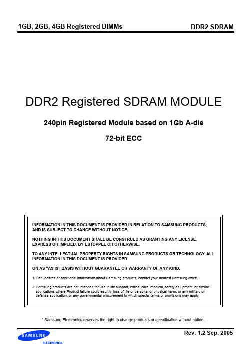
DDR2 Registered SDRAM MODULE 240pin Registered Module based on 1Gb A-die72-bit ECCINFORMATION IN THIS DOCUMENT IS PROVIDED IN RELATION TO SAMSUNG PRODUCTS,AND IS SUBJECT TO CHANGE WITHOUT NOTICE.NOTHING IN THIS DOCUMENT SHALL BE CONSTRUED AS GRANTING ANY LICENSE,EXPRESS OR IMPLIED, BY ESTOPPEL OR OTHERWISE,TO ANY INTELLECTUAL PROPERTY RIGHTS IN SAMSUNG PRODUCTS OR TECHNOLOGY. ALL INFORMATION IN THIS DOCUMENT IS PROVIDEDON AS "AS IS" BASIS WITHOUT GUARANTEE OR WARRANTY OF ANY KIND.1. For updates or additional information about Samsung products, contact your nearest Samsung office.2. Samsung products are not intended for use in life support, critical care, medical, safety equipment, or similarapplications where Product failure couldresult in loss of life or personal or physical harm, or any military ordefense application, or any governmental procurement to which special terms or provisions may apply.* Samsung Electronics reserves the right to change products or specification without notice.Table of Contents1.0 DDR2 Registered DIMM Ordering Information (4)2.0 Features (4)3.0 Address Configuration (4)4.0 Pin Configurations (Front side/Back side) (5)5.0 Pin Description (6)6.0 Input/Output Function Description (7)7.0 Functional Block Diagram (8)7.1 1GB, 128Mx72 Module (M393T2863AZ3/M393T2863AZA) (8)7.2 2GB, 256Mx72 Module (M393T5663AZ3/M393T5663AZA) (9)7.3 2GB, 256Mx72 Module (M393T5660AZ3/M393T5660AZA) (10)7.4 4GB, 512Mx72 Module (M393T5168AZ0/M393T5166AZA) (11)8.0 Absolute Maximum DC Ratings (12)9.0 AC & DC Operating Conditions (12)9.1 Operating Temperature Condition (13)9.2 Input DC Logic Level (13)9.3 Input AC Logic Level (13)9.4 AC Input Test Conditions (13)10.0 IDD Specification Parameters Definition (14)11.0 Operating Current Table(1-1) (15)11.1 M393T2863AZ3/M393T2863AZA : 1GB(128Mx8 *9) Module (15)11.2 M393T5663AZ3/M393T5663AZA : 2GB(128Mx8 *18) Module (15)11.3 M393T5660AZ3/M393T5660AZA : 2GB(256Mx4 *18) Module (16)11.4 M393T5168AZ0/M393T5166AZA : 4GB(st.512Mx4 *18) Module (16)12.0 Input/Output Capacitance (17)13.0 Electrical Characteristics & AC Timing for DDR2-667/533/400 (18)13.1 Refresh Parameters by Device Density (18)13.2 Speed Bins and CL, tRCD, tRP, tRC and tRAS for Corresponding Bin (18)13.3 Timing Parameters by Speed Grade (18)14.0 Physical Dimensions (20)14.1 128Mbx8 based 128Mx72 Module(1 Rank) (M393T2863AZ3/M393T2863AZA) (20)14.2 128Mbx8/256Mbx4 based 256Mx72 Module(2/1 Ranks)(M393T5663AZ3/M393T5663AZA/ M393T5660AZ3/M393T5660AZA) (21)14.3 st.512Mbx4 based 512Mx72 Module(2 Ranks) (M393T5168AZ0/M393T5166AZA) (22)15.0 240 Pin DDR2 Registered DIMM Clock Topology (23)Revision HistoryRevision Month Year History1.0July2005 - Initial Release1.1Aug.2005 - Revised IDD Current Values1.2Sep.2005 - Revised the Ordering InformationDDR2 Registered DIMM Ordering InformationPart Number Density Organization Component Composition Number of Rank Parity Register Height M393T2863AZ3-CD5/CC1GB128Mx72128Mx8(K4T1G084QA)*9EA1X30mm M393T2863AZA-CE6/D5/CC1GB128Mx72128Mx8(K4T1G084QA)*9EA1O30mm M393T5663AZ3-CD5/CC2GB256Mx72128Mx8(K4T1G084QA)*18EA2X30mm M393T5663AZA-CE6/D5/CC2GB256Mx72128Mx8(K4T1G084QA)*18EA2O30mm M393T5660AZ3-CD5/CC2GB256Mx72256Mx4(K4T1G044QA)*18EA1X30mm M393T5660AZA-CE6/D5/CC2GB256Mx72256Mx4(K4T1G044QA)*18EA1O30mm M393T5168AZ0-CD5/CC4GB512Mx72st.512Mx4(K4T2G064QA)*18EA2X30mm M393T5166AZA-CE6/D5/CC4GB512Mx72st.512Mx4(K4T2G264QA)*18EA2O30mm Note: “Z” of Part number(11th digit) stand for Lead-free products.Note: “3” of Part number(12th digit) stand for Dummy Pad PCB products.Note: "A" of Part number(12th digit) stand for Parity Register products.Features•Performance rangeE6(DDR2-667)D5(DDR2-533)CC(DDR2-400)UnitSpeed@CL3400400400MbpsSpeed@CL4533533400MbpsSpeed@CL5667533-MbpsCL-tRCD-tRP5-5-54-4-43-3-3CK•JEDEC standard 1.8V ± 0.1V Power Supply•V DDQ = 1.8V ± 0.1V•200 MHz f CK for 400Mb/sec/pin, 267MHz f CK for 533Mb/sec/pin, 333MHz f CK for 667Mb/sec/pin•8Banks•Posted CAS•Programmable CAS Latency: 3, 4, 5•Programmable Additive Latency: 0, 1 , 2 , 3 and 4•Write Latency(WL) = Read Latency(RL) -1•Burst Length: 4 , 8(Interleave/nibble sequential)•Programmable Sequential / Interleave Burst Mode•Bi-directional Differential Data-Strobe (Single-ended data-strobe is an optional feature)•Off-Chip Driver(OCD) Impedance Adjustment•On Die Termination with selectable values(50/75/150 ohms or disable)•PASR(Partial Array Self Refresh)•Average Refresh Period 7.8us at lower than a T CASE 85°C, 3.9us at 85°C < T CASE < 95 °C- support High Temperature Self-Refresh rate enable feature•Serial presence detect with EEPROM•DDR2 SDRAM Package: 68ball FBGA - 256Mx4/128Mx8, 56ball BGA - st.512Mbx4•All of Lead-free products are compliant for RoHSNote: For detailed DDR2 SDRAM operation, please refer to Samsung’s Device operation & Timing diagram..Address ConfigurationOrganization Row Address Column Address Bank Address Auto Precharge 256Mx4(1Gb) based Module A0-A13A0-A9, A11BA0-BA2A10128Mx8(1Gb) based Module A0-A13A0-A9BA0-BA2A10NC = No Connect, RFU = Reserved for Future Use1. RESET (Pin 18) is connected to both OE of PLL and Reset of register.2. The Test pin (Pin 102) is reserved for bus analysis probes and is not connected on normal memory modules (DIMMs)3. NC/Err_Out ( Pin 55) and NC/Par_In (Pin 68) are for optional function to check address and command parity.4. CKE1,S1 Pin is used for double side Registered DIMM.Pin Front Pin Back Pin Front Pin Back Pin Front Pin Back Pin Front Pin Back 1V REF 121V SS 31DQ19151V SS 61A4181V DDQ 91V SS 211DM5/DQS142V SS 122DQ432V SS 152DQ2862V DDQ 182A392DQS5212NC/DQS143DQ0123DQ533DQ24153DQ2963A2183A193DQS5213V SS 4DQ1124V SS 34DQ25154V SS 64V DD184V DD94V SS 214DQ465V SS 125DM0/DQS935V SS 155DM3/DQS12KEY95DQ42215DQ476DQS0126NC/DQS936DQS3156NC/DQS1265V SS 185CK096DQ43216V SS 7DQS0127V SS 37DQS3157V SS 66V SS 186CK097V SS 217DQ528V SS 128DQ638V SS 158DQ3067V DD 187V DD 98DQ48218DQ539DQ2129DQ739DQ26159DQ3168NC/Par_In 188A099DQ49219V SS 10DQ3130V SS 40DQ27160V SS 69V DD 189V DD 100V SS 220RFU 11V SS 131DQ1241V SS 161CB470A10/AP 190BA1101SA2221RFU 12DQ8132DQ1342CB0162CB571BA0191V DDQ 102NC(TEST)222V SS 13DQ9133V SS 43CB1163V SS 72V DDQ 192RAS 103V SS 223DM6/DQS1514V SS 134DM1/DQS1044V SS 164DM8/DQS1773WE 193S0104DQS6224NC/DQS1515DQS1135NC/DQS1045DQS8165NC/DQS1774CAS 194V DDQ 105DQS6225V SS 16DQS1136V SS 46DQS8166V SS 75V DDQ 195ODT0106V SS 226DQ5417V SS 137RFU 47V SS 167CB676S14196A13107DQ50227DQ5518RESET 138RFU 48CB2168CB777ODT1197V DD 108DQ51228V SS 19NC 139V SS 49CB3169V SS 78V DDQ 198V SS 109V SS 229DQ6020V SS 140DQ1450V SS 170V DDQ 79V SS 199DQ36110DQ56230DQ6121DQ10141DQ1551V DDQ 171CKE1480DQ32200DQ37111DQ57231V SS 22DQ11142V SS 52CKE0172V DD 81DQ33201V SS 112V SS 232DM7/DQS1623V SS 143DQ2053V DD 173NC 82V SS 202DM4/DQS13113DQS7233NC/DQS1624DQ16144DQ2154BA2174NC 83DQS4203NC/DQS13114DQS7234V SS 25DQ17145V SS 55NC/Err_Out 175V DDQ 84DQS4204V SS 115V SS 235DQ6226V SS 146DM2/DQS1156V DDQ 176A1285V SS 205DQ38116DQ58236DQ6327DQS2147NC/DQS1157A11177A986DQ34206DQ39117DQ59237V SS 28DQS2148V SS 58A7178V DD 87DQ35207V SS 118V SS 238VDDSPD 29V SS 149DQ2259V DD 179A888V SS 208DQ44119SDA 239SA030DQ18150DQ2360A5180A689DQ40209DQ45120SCL240SA190DQ41210V SS Pin Configurations (Front side/Back side)* The VDD and VDDQ pins are tied to the single power-plane on PCB.Pin Name DescriptionPin Name Description CK0Clock Inputs, positive line ODT0~ODT1On die termination CK0Clock inputs, negative line DQ0~DQ63Data Input/OutputCKE0, CKE1Clock Enables CB0~CB7Data check bits Input/Output RAS Row Address Strobe DQS0~DQS8Data strobesCAS Column Address Strobe DQS0~DQS8Data strobes, negative line WE Write Enable DM(0~8), DQS(9~17)Data Masks / Data strobes (Read)S0, S1Chip Selects DQS9~DQS17Data strobes (Read), negative line A0~A9, A11~A13Address InputsRFU Reserved for Future Use A10/AP Address Input/Autoprecharge NC No ConnectBA0~BA2DDR2 SDRAM Bank AddressTEST Memory bus test tool(Not Connect and Not Useable on DIMMs)SCL Serial Presence Detect (SPD) Clock Input V DD Core Power SDA SPD Data Input/Output V DDQ I/O Power SA0~SA2SPD addressV SS GroundPar_In Parity bit for the Address and Control bus V REF Input/Output Reference Err_Out Parity error found in the Address and Control bus V DDSPDSPD PowerRESETRegister and PLL control pinPin DescriptionSymbol Type DescriptionCK0Input Positive line of the differential pair of system clock inputs that drives input to the on-DIMM PLL.CK0Input Negative line of the differential pair of system clock inputs that drives the input to the on-DIMM PLL.CKE0~CKE1Input Activates the SDRAM CK signal when high and deactivates the CK signal when low. By deactivating the clocks, CKE low initiates the Power Down mode, or the Self Refresh mode.S0~S1Input Enables the associated SDRAM command decoder when low and disables decoder when high. When decoder is dis-abled, new commands are ignored but previous operations continue.These input signals also disable all outputs (except CKE and ODT) of the register(s) on the DIMM when both inputs are high.ODT0~ODT1Input I/O bus impedance control signals.RAS, CAS, WE Input When sampled at the positive rising edge of the clock, CAS, RAS, and WE define the operation to be executed by the SDRAM.V REF Supply Reference voltage for SSTL_18 inputsV DDQ Supply Isolated power supply for the DDR SDRAM output buffers to provide improved noise immunity BA0~BA2Input Selects which SDRAM bank of eight is activated.A0~A9,A10/APA11~A13Input During a Bank Activate command cycle, Address defines the row address.During a Read or Write command cycle, Address defines the column address. In addition to the column address, AP is used to invoke autoprecharge operation at the end of the burst read or write cycle. If AP is high, autoprecharge is selected and BA0, BA1, BA2 defines the bank to be precharged. If AP is low, autoprecharge is disabled. During a Precharge com-mand cycle, AP is used in conjunction with BA0, BA1, BA2 to control which bank(s) to precharge. If AP is high, all banks will be precharged regardless of the state of BA0 or BA1 or BA2. If AP is low, BA0 and BA1 and BA2 are used to define which bank to precharge.DQ0~63,CB0~CB7In/Out Data and Check Bit Input/Output pinsDM0~DM8Input Masks write data when high, issued concurrently with input data. Both DM and DQ have a write latency of one clock once the write command is registered into the SDRAM.V DD, V SS Supply Power and ground for the DDR SDRAM input buffers and core logicDQS0~DQS17In/Out Positive line of the differential data strobe for input and output data.DQS0~DQS17In/Out Negative line of the differential data strobe for input and output data.SA0~SA2Input These signals are tied at the system planar to either V SS or V DDSPD to configure the serial SPD EEPROM address range.SDA In/Out This bidirectional pin is used to transfer data into or out of the SPD EEPROM. A resistor must be connected from the SDA bus line to V DDSPD to act as a pullup.SCL Input This signal is used to clock data into and out of the SPD EEPROM. A resistor may be connected from the SCL bus time to V DDSPD to act as a pullup.V DDSPD Supply Serial EEPROM positive power supply (wired to a separate power pin at the connector which supports from 1.7 Volt to 3.6 Volt operation).RESET Input The RESET pin is connected to the RST pin on the register and to the OE pin on the PLL. When low, all register outputs will be driven low and the PLL clocks to the DRAMs and register(s) will be set to low level (The PLL will remain synchro-nized with the input clock )Par_In Input Parity bit for the Address and Control bus. ( “1 “ : Odd, “0 “ : Even) Err_Out Input Parity error found in the Address and Control busTEST In/Out Used by memory bus analysis tools (unused on memory DIMMs) Input/Output Function Description(populated as 1 rank of x8 DDR2 SDRAMs)1GB, 128Mx72 Module (M393T2863AZ3/M393T2863AZA)RS0DQS0DQS0DM0/DQS9NC/DQS9DM/ RDQS NU/RDQSCS DQS DQSDQ0 DQ1 DQ2 DQ3 DQ4 DQ5 DQ6 DQ7I/O 0I/O 1I/O 2I/O 3I/O 4I/O 5I/O 6I/O 7D0DQS1DQS1DM1/DQS10 NC/DQS10DM/ RDQS NU/RDQSCS DQS DQSDQ8 DQ9 DQ10 DQ11 DQ12 DQ13 DQ14 DQ15I/O 0I/O 1I/O 2I/O 3I/O 4I/O 5I/O 6I/O 7D1DQS2DQS2DM2/DQS11 NC/DQS11DM/ RDQS NU/RDQSCS DQS DQSDQ16 DQ17 DQ18 DQ19 DQ20 DQ21 DQ22 DQ23I/O 0I/O 1I/O 2I/O 3I/O 4I/O 5I/O 6I/O 7D2DQS3DQS3DM3/DQS12 NC/DQS12DM/ RDQS NU/RDQSCS DQS DQSDQ24 DQ25 DQ26 DQ27 DQ28 DQ29 DQ30 DQ31I/O 0I/O 1I/O 2I/O 3I/O 4I/O 5I/O 6I/O 7D3DQS8DQS8DM8/DQS17 NC/DQS17DM/ RDQS NU/RDQSCS DQS DQSCB0 CB1 CB2 CB3 CB4 CB5 CB6 CB7I/O 0I/O 1I/O 2I/O 3I/O 4I/O 5I/O 6I/O 7D8DQS4DQS4DM4/DQS13NC/DQS13DM/RDQSNU/RDQSCS DQS DQSDQ32DQ33DQ34DQ35DQ36DQ37DQ38DQ39I/O 0I/O 1I/O 2I/O 3I/O 4I/O 5I/O 6I/O 7D4DQS5DQS5DM5/DQS14NC/DQS14DM/RDQSNU/RDQSCS DQS DQSDQ40DQ41DQ42DQ43DQ44DQ45DQ46DQ47I/O 0I/O 1I/O 2I/O 3I/O 4I/O 5I/O 6I/O 7D5DQS6DQS6DM6/DQS15NC/DQS15DM/RDQSNU/RDQSCS DQS DQSDQ48DQ49DQ50DQ51DQ52DQ53DQ54DQ55I/O 0I/O 1I/O 2I/O 3I/O 4I/O 5I/O 6I/O 7D6DQS7DQS7DM7/DQS16NC/DQS16DM/RDQSNU/RDQSCS DQS DQSDQ56DQ57DQ58DQ59DQ60DQ61DQ62DQ63I/O 0I/O 1I/O 2I/O 3I/O 4I/O 5I/O 6I/O 7D7A0Serial PDA1A2SA0SA1SA2SCL SDAV SS D0 - D8V DD/V DDQ D0 - D8D0 - D8VREFV DDSPD Serial PDWPNotes :1. DQ-to-I/O wiring may be changed within a byte.2. DQ/DQS/DM/CKE/S relationships must be maintained as shown.3. Unless otherwise noted, resister values are 22 Ohms1:1REGISTERRSTS0*BA0-BA2A0-A13RASCASWECKE0ODT0RESETPCK7PCK7RSO-> CS : DDR2 SDRAMs D0-D8RBA0-RBA2 -> BA0-BA2 : DDR2 SDRAMs D0-D8RA0-RA13 -> A0-A13 : DDR2 SDRAMs D0-D8RRAS -> RAS : DDR2 SDRAMs D0-D8RCAS -> CAS : DDR2 SDRAMs D0-D8RWE -> WE : DDR2 SDRAMs D0-D8RCKE0 -> CKE : DDR2 SDRAMs D0-D8RODT0 -> ODT0 : DDR2 SDRAMs D0-D8PLLOECK0CK0RESETPCK0-PCK6, PCK8, PCK9 -> CK : DDR2 SDRAMs D0-D8PCK0-PCK6, PCK8, PCK9 -> CK : DDR2 SDRAMs D0-D8PCK7 -> CK : RegisterPCK7 -> CK : Register* S0 connects to DCS and VDD connects to CSR on the register.Functional Block DiagramSignals for Address and Command Parity Function (M393T2863AZA)V SSV SS PAR_IN C0C1PPOQERR Err_Out RegisterPAR_IN100K ohmsThe resistors on Par_In, A13, A14, A15, BA2 and the signal line of Err_Out refer to the section: "Register Options for Unused Address inputs"RS0DQS0DQS0DM0/DQS9NC/DQS9DM/RDQS NU/RDQSCS DQS DQSDQ0DQ1DQ2DQ3DQ4DQ5DQ6DQ7I/O 0I/O 1I/O 2I/O 3I/O 4I/O 5I/O 6I/O 7D0DQS1DQS1DM1/DQS10NC/DQS10DM/RDQS NU/RDQSCS DQS DQSDQ8DQ9DQ10DQ11DQ12DQ13DQ14DQ15I/O 0I/O 1I/O 2I/O 3I/O 4I/O 5I/O 6I/O 7D1DQS2DQS2DM2/DQS11NC/DQS11DM/RDQS NU/RDQSCS DQS DQSDQ16DQ17DQ18DQ19DQ20DQ21DQ22DQ23I/O 0I/O 1I/O 2I/O 3I/O 4I/O 5I/O 6I/O 7D2DQS3DQS3DM3/DQS12NC/DQS12DM/RDQS NU/RDQSCS DQS DQSDQ24DQ25DQ26DQ27DQ28DQ29DQ30DQ31I/O 0I/O 1I/O 2I/O 3I/O 4I/O 5I/O 6I/O 7D3DQS8DQS8DM8/DQS17NC/DQS17DM/RDQS NU/RDQSCS DQS DQSCB0CB1CB2CB3CB4CB5CB6CB7I/O 0I/O 1I/O 2I/O 3I/O 4I/O 5I/O 6I/O 7D8DQS4DQS4DM4/DQS13NC/DQS13DM/RDQS NU/RDQSCS DQS DQSDQ32DQ33DQ34DQ35DQ36DQ37DQ38DQ39I/O 0I/O 1I/O 2I/O 3I/O 4I/O 5I/O 6I/O 7D4DQS5DQS5DM5/DQS14NC/DQS14DM/RDQS NU/RDQSCS DQS DQSDQ40DQ41DQ42DQ43DQ44DQ45DQ46DQ47I/O 0I/O 1I/O 2I/O 3I/O 4I/O 5I/O 6I/O 7D5DQS6DQS6DM6/DQS15NC/DQS15DM/RDQS NU/RDQSCS DQS DQSDQ48DQ49DQ50DQ51DQ52DQ53DQ54DQ55I/O 0I/O 1I/O 2I/O 3I/O 4I/O 5I/O 6I/O 7D6DQS7DQS7DM7/DQS16NC/DQS16DM/RDQS NU/RDQSCS DQS DQSDQ56DQ57DQ58DQ59DQ60DQ61DQ62DQ63I/O 0I/O 1I/O 2I/O 3I/O 4I/O 5I/O 6I/O 7D7DM/RDQS NU/RDQSCS DQS DQSI/O 0I/O 1I/O 2I/O 3I/O 4I/O 5I/O 6I/O 7D9DM/RDQS NU/RDQSCS DQS DQSI/O 0I/O 1I/O 2I/O 3I/O 4I/O 5I/O 6I/O 7D10DM/RDQS NU/RDQSCS DQS DQSI/O 0I/O 1I/O 2I/O 3I/O 4I/O 5I/O 6I/O 7D11DM/RDQS NU/RDQSCS DQS DQSI/O 0I/O 1I/O 2I/O 3I/O 4I/O 5I/O 6I/O 7D12DM/RDQS NU/RDQSCS DQS DQSI/O 0I/O 1I/O 2I/O 3I/O 4I/O 5I/O 6I/O 7D17DM/RDQS NU/RDQSCS DQS DQSI/O 0I/O 1I/O 2I/O 3I/O 4I/O 5I/O 6I/O 7D13DM/RDQS NU/RDQSCS DQS DQSI/O 0I/O 1I/O 2I/O 3I/O 4I/O 5I/O 6I/O 7D14DM/RDQS NU/RDQSCS DQS DQSI/O 0I/O 1I/O 2I/O 3I/O 4I/O 5I/O 6I/O 7D15DM/RDQS NU/RDQSCS DQS DQSI/O 0I/O 1I/O 2I/O 3I/O 4I/O 5I/O 6I/O 7D16RS1A0Serial PDA1A2SA0SA1SA2SCLSDAV SSD0 - D17V DD /V DDQ D0 - D17D0 - D17VREF V DDSPDSerial PD WP Notes :1. DQ-to-I/O wiring may be changed per nibble.2. Unless otherwise noted, resister values are 22 Ohms3. RS0 and RS1 alternate between the back and front sides of the DIMM1:2R E G I S T E RRSTS1*BA0-BA2A0-A13RAS CAS WE CKE0CKE1RESET**PCK7**PCK7**RS1-> CS : DDR2 SDRAMs D9-D17RBA0-RBA2 -> BA0-BA2: DDR2 SDRAMs D0-D17RA0-RA13 -> A0-A13 : DDR2 SDRAMs D0-D17RRAS -> RAS : DDR2 SDRAMs D0-D17RCAS -> CAS : DDR2 SDRAMs D0-D17RWE -> WE : DDR2 SDRAMs D0-D17RCKE0 -> CKE : DDR2 SDRAMs D0-D8RCKE1 -> CKE : DDR2 SDRAMs D9-D17P L LOECK0CK0RESETPCK0-PCK6, PCK8, PCK9 -> CK : DDR2 SDRAMs D0-D17PCK0-PCK6, PCK8, PCK9 -> CK : DDR2 SDRAMs D0-D17PCK7 -> CK : Register PCK7 -> CK : RegisterODT0ODT1RODT0 -> ODT0 : DDR2 SDRAMs D0-D8RODT1 -> ODT1 : DDR2 SDRAMs D9-D17S0*RSO-> CS : DDR2 SDRAMs D0-D8(populated as 2 rank of x8 DDR2 SDRAMs)2GB, 256Mx72 Module (M393T5663AZ3/M393T5663AZA)* S0 connects to DCS and S0 connects to CSR on a Register,S1 connects to DCS and S0 connects to CSR on another Register.** RESET, PCK7 and PCK7 connects to both Registers. Other signals connect to one of two Registers.Signals for Address and Command Parity Function (M393T5663AZA)V SS V DDPAR_IN C0C1PPO QERRRegister APAR_IN 100K ohmsThe resistors on Par_In, A13, A14, A15, BA2 and the signal line of Err_Out refer to the section: "Register Options for Unused Address inputs"V DD V DDC0C1PPO QERRErr_OutRegister BPAR_INVSSRS0DQS0DQS0DM CS DQS DQSDQ0 DQ1 DQ2 DQ3I/O 0I/O 1I/O 2I/O 3D0DM0/DQS9NC/DQS9DM CS DQS DQSDQ4DQ5DQ6DQ7I/O 0I/O 1I/O 2I/O 3D9DQS1DQS1DM CS DQS DQSDQ8 DQ9 DQ10 DQ11I/O 0I/O 1I/O 2I/O 3D1DM1/DQS10NC/DQS10DM CS DQS DQSDQ12DQ13DQ14DQ15I/O 0I/O 1I/O 2I/O 3D10DQS2DQS2DM CS DQS DQSDQ16 DQ17 DQ18 DQ19I/O 0I/O 1I/O 2I/O 3D2DM2/DQS11NC/DQS11DM CS DQS DQSDQ20DQ21DQ22DQ23I/O 0I/O 1I/O 2I/O 3D11DQS3DQS3DM CS DQS DQSDQ24 DQ25 DQ26 DQ27I/O 0I/O 1I/O 2I/O 3D3DM3/DQS12NC/DQS12DM CS DQS DQSDQ28DQ29DQ30DQ31I/O 0I/O 1I/O 2I/O 3D12DQS5DQS5DM CS DQS DQSDQ40 DQ41 DQ42 DQ43I/O 0I/O 1I/O 2I/O 3D5DM5/DQS14NC/DQS14DM CS DQS DQSDQ44DQ45DQ46DQ47I/O 0I/O 1I/O 2I/O 3D14DQS4DQS4DM CS DQS DQSDQ32 DQ33 DQ34 DQ35I/O 0I/O 1I/O 2I/O 3D4DM4/DQS13NC/DQS13DM CS DQS DQSDQ36DQ37DQ38DQ39I/O 0I/O 1I/O 2I/O 3D13DQS6DQS6DM CS DQS DQSDQ48 DQ49 DQ50 DQ51I/O 0I/O 1I/O 2I/O 3D6DM6/DQS15NC/DQS15DM CS DQS DQSDQ52DQ53DQ54DQ55I/O 0I/O 1I/O 2I/O 3D15DQS8DQS8DM CS DQS DQSCB0 CB1 CB2 CB3I/O 0I/O 1I/O 2I/O 3D8DM8/DQS17NC/DQS17DM CS DQS DQSCB4CB5CB6CB7I/O 0I/O 1I/O 2I/O 3D17DQS7DQS7DM CS DQS DQSDQ56 DQ57 DQ58 DQ59I/O 0I/O 1I/O 2I/O 3D7DM7DQS16NC/DQS16DM CS DQS DQSDQ60DQ61DQ62DQ63I/O 0I/O 1I/O 2I/O 3D16A0Serial PDA1A2SA0SA1SA2SCL SDAV SS D0 - D17V DD/V DDQ D0 - D17D0 - D17VREFV DDSPD Serial PDWPNotes :1. DQ-to-I/O wiring may be changed per nibble.2. Unless otherwise noted, resister values are 22 Ohms 1:2REGISTERRSTS0*BA0-BA2A0-A13RASCASWECKE0ODT0RESET**PCK7** PCK7**RSO-> CS : DDR2 SDRAMs D0-D17RBA0-RBA2 -> BA0-BA2 : DDR2 SDRAMs D0-D17RA0-RA13 -> A0-A13 : DDR2 SDRAMs D0-D17RRAS -> RAS : DDR2 SDRAMs D0-D17RCAS -> CAS : DDR2 SDRAMs D0-D17RWE -> WE : DDR2 SDRAMs D0-D17RCKE0 -> CKE : DDR2 SDRAMs D0-D17RODT0 -> ODT0 : DDR2 SDRAMs D0-D17PLLOECK0CK0RESETPCK0-PCK6, PCK8, PCK9 -> CK : DDR2 SDRAMs D0-D8PCK0-PCK6, PCK8, PCK9 -> CK : DDR2 SDRAMs D0-D8PCK7 -> CK : RegisterPCK7 -> CK : Register(populated as 1 rank of x4 DDR2 SDRAMs)2GB, 256Mx72 Module (M393T5660AZ3/M393T5660AZA)* S0 connects to DCS of Register1, CSR of Register2. CSR of reg-ister 1 and DCS of register 2 connects to VDD.** RESET, PCK7 and PCK7 connects to both Registers. Other sig-nals connect to one of two Registers.Signals for Address and Command Parity Function (M393T5660AZA)V SSV DDPAR_INC0C1PPOQERRRegister APAR_IN100K ohmsThe resistors on Par_In, A13, A14, A15, BA2 and thesignal line of Err_Out refer to the section: "RegisterOptions for Unused Address inputs"V DDV DDC0C1PPOQERR Err_OutRegister BPAR_IN(populated as 2 rank of x4 DDR2 SDRAMs)A0Serial PDA1A2SA0SA1SA2SCLSDAV SSD0 - D35V DD /V DDQ D0 - D35D0 - D35VREF V DDSPDSerial PD WP P L LOECK0CK0RESET PCK0-PCK6, PCK8, PCK9 -> CK : DDR2 SDRAMs D0-D35PCK0-PCK6, PCK8, PCK9 -> CK : DDR2 SDRAMs D0-D35PCK7 -> CK : Register PCK7 -> CK : Register1:2R E G I S T E RRSTS1*BA0-BA2A0-A13RAS CAS WE CKE0CKE1RESET**PCK7**PCK7**RS1-> CS : DDR2 SDRAMs D18-D35RBA0-RBA2 -> BA0-BA2 : DDR2 SDRAMs D0-D35RA0-RA13 -> A0-A13 : DDR2 SDRAMs D0-D35RRAS -> RAS : DDR2 SDRAMs D0-D35RCAS -> CAS : DDR2 SDRAMs D0-D35RWE -> WE : DDR2 SDRAMs D0-D35RCKE0 -> CKE : DDR2 SDRAMs D0-D17RCKE1 -> CKE : DDR2 SDRAMs D18-D35ODT0ODT1RODT0 -> ODT0 : DDR2 SDRAMs D0-D17RODT1 -> ODT1 : DDR2 SDRAMs D18-D35S0*RSO-> CS : DDR2 SDRAMs D0-D174GB, 512Mx72 Module (M393T5168AZ0/M393T5166AZA)* S0 connects to DCS and S0 connects to CSR on a Register,S1 connects to DCS and S0 connects to CSR on another Register.** RESET, PCK7 and PCK7 connects to both Registers. Other signals connect to one of two Registers.VSS RS0DQS0DQS0DMCSDQS DQSDQ0DQ1DQ2DQ3I/O 0I/O 1I/O 2I/O 3D0DM0/DQS9NC/DQS9DMCSDQS DQSDQ4DQ5DQ6DQ7I/O 0I/O 1I/O 2I/O 3D9DQS1DQS1DM CS DQS DQS DQ8DQ9DQ10DQ11I/O 0I/O 1I/O 2I/O 3D1DM1/DQS10NC/DQS10DM CS DQS DQS DQ12DQ13DQ14DQ15I/O 0I/O 1I/O 2I/O 3D10DQS2DQS2DM CS DQS DQS DQ16DQ17DQ18DQ19I/O 0I/O 1I/O 2I/O 3D2DM2/DQS11NC/DQS11DM CS DQS DQS DQ20DQ21DQ22DQ23I/O 0I/O 1I/O 2I/O 3D11DQS3DQS3DM CS DQS DQS DQ24DQ25DQ26DQ27I/O 0I/O 1I/O 2I/O 3D3DM3/DQS12NC/DQS12DM CS DQS DQS DQ28DQ29DQ30DQ31I/O 0I/O 1I/O 2I/O 3D12DQS5DQS5DM CS DQS DQS DQ40DQ41DQ42DQ43I/O 0I/O 1I/O 2I/O 3D5DM5/DQS14NC/DQS14DM CS DQS DQS DQ44DQ45DQ46DQ47I/O 0I/O 1I/O 2I/O 3D14DQS4DQS4DM CS DQS DQS DQ32DQ33DQ34DQ35I/O 0I/O 1I/O 2I/O 3D4DM4/DQS13NC/DQS13DM CS DQS DQS DQ36DQ37DQ38DQ39I/O 0I/O 1I/O 2I/O 3D13DQS6DQS6DM CS DQS DQS DQ48DQ49DQ50DQ51I/O 0I/O 1I/O 2I/O 3D6DM6/DQS15NC/DQS15DM CS DQS DQS DQ52DQ53DQ54DQ55I/O 0I/O 1I/O 2I/O 3D15DQS8DQS8DM CS DQS DQS CB0CB1CB2CB3I/O 0I/O 1I/O 2I/O 3D8DM8/DQS17NC/DQS17DM CS DQS DQS CB4CB5CB6CB7I/O 0I/O 1I/O 2I/O 3D17DQS7DQS7DM CS DQS DQS DQ56DQ57DQ58DQ59I/O 0I/O 1I/O 2I/O 3D7DM7DQS16NC/DQS16DM CS DQS DQS DQ60DQ61DQ62DQ63I/O 0I/O 1I/O 2I/O 3D16DM/CSDQS DQSI/O 0I/O 1I/O 2I/O 3D18DM/CS DQS DQS I/O 0I/O 1I/O 2I/O 3D19DM/CS DQS DQS I/O 0I/O 1I/O 2I/O 3D20DM CS DQS DQS I/O 0I/O 1I/O 2I/O 3D21DM CS DQS DQS I/O 0I/O 1I/O 2I/O 3D23DM CS DQS DQS I/O 0I/O 1I/O 2I/O 3D22DM CS DQS DQS I/O 0I/O 1I/O 2I/O 3D24DM CS DQS DQS I/O 0I/O 1I/O 2I/O 3D26DM CS DQS DQS I/O 0I/O 1I/O 2I/O 3D25DMCSDQS DQSI/O 0I/O 1I/O 2I/O 3D27DM CS DQS DQSI/O 0I/O 1I/O 2I/O 3D28DM CS DQS DQSI/O 0I/O 1I/O 2I/O 3D29DM CS DQS DQSI/O 0I/O 1I/O 2I/O 3D30DM CS DQS DQSI/O 0I/O 1I/O 2I/O 3D32DM CS DQS DQSI/O 0I/O 1I/O 2I/O 3D31DM CS DQS DQSI/O 0I/O 1I/O 2I/O 3D33DM CS DQS DQSI/O 0I/O 1I/O 2I/O 3D35DM CS DQS DQSI/O 0I/O 1I/O 2I/O 3D34RS1Signals for Address and Command The resistors on Par_In, A13, A14, A15, BA2and the signal line of Err_Out refer to the sec-tion: "Register Options for Unused Address inputs"PAR_INErr_Out100K ohmsV SS V DDC0C1PPO QERRRegister A1PAR_INV DD V DDC0C1PPO QERRRegister B1PAR_INV SS V DDC0C1PPO QERRRegister A2PAR_INV DD V DDC0C1PPO QERRRegister B2PAR_INParity Function (M393T5166AZA)Register A1 and A2 share the a part of Add/Cmd input signal set.Register B1 and B2 share the rest part of Add/Cmd input signal set.Recommended DC Operating Conditions (SSTL - 1.8)Note : There is no specific device V DD supply voltage requirement for SSTL-1.8 compliance. However under all conditions V DDQ must be less than or equalto V DD .1. The value of V REF may be selected by the user to provide optimum noise margin in the system. Typically the value of V REF is expected to be about 0.5 x V DDQ of the transmitting device and V REF is expected to track variations in V DDQ .2. Peak to peak AC noise on V REF may not exceed +/-2% V REF (DC).3. V TT of transmitting device must track V REF of receiving device.4. AC parameters are measured with V DD , V DDQ and V DDL tied together.Symbol ParameterRatingUnits NotesMin.Typ. Max.V DD Supply Voltage 1.7 1.8 1.9V V DDL Supply Voltage for DLL 1.7 1.8 1.9V 4V DDQ Supply Voltage for Output 1.7 1.8 1.9V 4V REF Input Reference Voltage 0.49*V DDQ 0.50*V DDQ0.51*V DDQ mV 1,2V TTTermination VoltageV REF -0.04V REFV REF +0.04V3 Note :1. Stresses greater than those listed under “Absolute Maximum Ratings” may cause permanent damage to the device. This is a stress rating only and functional operation of the device at these or any other conditions above those indicated in the operational sections of this specification is not implied. Exposure to absolute maximum rating conditions for extended periods may affect reliability.2. Storage Temperature is the case surface temperature on the center/top side of the DRAM. For the measurement conditions, please refer to JESD51-2standard.Symbol ParameterRating Units Notes V DD Voltage on V DD pin relative to V SS - 1.0 V ~ 2.3 V V 1V DDQ Voltage on V DDQ pin relative to V SS - 0.5 V ~ 2.3 V V 1V DDL Voltage on V DDL pin relative to V SS - 0.5 V ~ 2.3 V V 1V IN, V OUT Voltage on any pin relative to V SS - 0.5 V ~ 2.3 V V1T STGStorage Temperature-55 to +100°C 1, 2AC & DC Operating ConditionsAbsolute Maximum DC Ratings。
csc929芯片资料

csc929芯片资料【原创版】目录1.引言2.CSC929 芯片概述3.CSC929 芯片的功能特点4.CSC929 芯片的技术参数5.CSC929 芯片的应用领域6.结论正文【引言】随着科技的不断发展,芯片在各个领域的应用越来越广泛,性能要求也越来越高。
本文将为您介绍一款名为 CSC929 的芯片,并详细阐述其功能特点、技术参数以及应用领域。
【CSC929 芯片概述】CSC929 是一款高度集成的芯片,具有低功耗、高性能、多功能等特点。
该芯片主要应用于通信、计算机、消费电子等领域,可满足各种复杂应用场景的需求。
【CSC929 芯片的功能特点】1.低功耗:CSC929 芯片采用了先进的工艺制程,能够在保证性能的同时有效降低功耗,提高设备的续航表现。
2.高性能:CSC929 芯片具备高速运算能力,可实现高速数据传输和处理,满足各种复杂应用场景的需求。
3.多功能:CSC929 芯片集成了多种功能,如音频处理、图像处理、存储控制等,可减少系统中的芯片数量,提高系统的稳定性和可靠性。
【CSC929 芯片的技术参数】CSC929 芯片的主要技术参数如下:1.处理器:高性能处理器,主频可达 XX MHz。
2.内存:集成 XX MB 内存,支持 DDRX 接口。
3.存储:支持 SATA、PCIe 等存储接口,可实现高速存储。
4.显示:支持高清显示,最大分辨率可达 XX。
5.通信:支持多种通信接口,如 Gigabit Ethernet、USB 等。
6.音频:集成高性能音频处理器,支持多通道音频处理。
7.安全:支持硬件加密,保障数据安全。
【CSC929 芯片的应用领域】CSC929 芯片广泛应用于以下领域:1.通信设备:如路由器、交换机等。
2.消费电子:如智能电视、智能家居设备等。
3.计算机:如台式机、笔记本电脑等。
4.工业控制:如工业自动化设备、智能机器人等。
【结论】CSC929 芯片凭借其低功耗、高性能、多功能等优点,在通信、计算机、消费电子等领域具有广泛的应用前景。
ASTM标准.D3930

A376/A376M Specification for Seamless Austenitic Steel Pipe for High-Temperature Central-Station Service2D905Test Method for Strength Properties of Adhesive Bonds in Shear by Compression Loading3D1002Test Method for Apparent Shear Strength of Single-Lap-Joint Adhesively Bonded Metal Specimens by Ten-sion Loading(Metal-to-Metal)3D2294Test Method for Creep Properties of Adhesives in Shear by Tension Loading(Metal-to-Metal)3D2339Test Method for Strength Properties of Adhesives in Two-Ply Wood Construction in Shear by Tension Loading3 D3110Specification for Adhesives Used in Laminate Joints for Nonstructural Glued Lumber Products3D3632Practice for Accelerated Aging of Adhesive Joints by the Oxygen-Pressure Method3D3931Test Method for Determining Strength of Gap-Filling Adhesive Bonds in Shear by Compression Load-ing3D4300Test Methods for Ability of Adhesive Films to Support or Resist the Growth of Fungi33.Terminology3.1Definitions—Many terms in this specification are de-fined in Terminology D907.3.1.1creep,n—in an adhesive,the time-dependent increase in strain resulting from a sustained stress.3.1.2gap-filling adhesive,n—an adhesive capable of form-ing and maintaining a bond between surfaces that are not close-fitting.3.1.2.1Discussion—Closefitting is relative to a given material and industry;for example,standards in construction differ from standards in electronics.Some adhesives will bond by bridging without completelyfilling the gap;others byfilling the gap completely.3.2Definitions of Terms Specific to This Standard:3.2.1manufactured home4—a structure,transportable in one or more sections which in the traveling mode is8body feet or more in width or40body feet or more in length or when erected on site,is320or more square feet and which is built on a permanent chassis and designed to be used as a dwelling with or without a permanent foundation when connected to the required utilities,and includes the plumbing,heating,air-conditioning,and electrical systems contained therein.Calcu-lations used to determine the number of square feet in a structure will be based on the structure’s exterior dimensions measured at the largest horizontal projections when erected on site.These dimensions will include all expandable rooms,bay windows,cabinets,and other projections containing interior space.3.2.2semi-structural adhesive—an adhesive capable of transferring required loads between adherends and which deforms a maximum of0.050in.(1.27mm)under static load when tested in accordance with Test9,Section23.3.2.3structural adhesive—an adhesive capable of transfer-ring required loads between adherends and which deforms a maximum of0.006in.(0.15mm)under static load when tested in accordance with Test9,Section23.3.2.4total deformation—the total dimensional change with time of a material under constant load,and consisting of the initial instantaneous elastic or rapid deformation and the slower time dependent deformation or creep.3.2.5Type1adhesive—an adhesive that will retain its bond integrity when the joint is repeatedly wetted and dried.3.2.6Type2adhesive—an adhesive intended for use in protected locations but that will maintain its bond integrity when the bond is subjected to occasional wetting.3.2.7Type3adhesive—an adhesive intended for use in interior locations,but that will maintain its bond integrity during conditions of high humidity.N OTE1—The following ASTM standards may be referred to for other terms used in this specification:D9,Terms Relating to Timber;D907, Terms Relating to Adhesives;D1165,Nomenclature of Domestic Hard-woods and Softwoods;E6,Terms Relating to Methods of Mechanical Testing;and E41,Terms Relating to Conditioning.4.Classification4.1Adhesives shall be classified as follows(see Table1): 4.1.1By resistance to deformation as:4.1.1.1Group A,Structural;or Group B,Semistructural, 4.1.2By resistance to water and water vapor as:4.1.2.1Type1,Type2,or Type3,and4.1.3By gap-filling ability.4.1.3.1Those adhesives tested in accordance with Test3, Section17,shall carry the designation G/F.5.Significance and Use5.1Shear Strength—This specification requires determin-ing ultimate shear strength of adhesive bonds under a variety of conditions of assembly and service.5.2Gap-Filling Ability—Gap-filling adhesives must be ca-pable of maintaining a bond between construction members whose faying surfaces are not closely matched.The gap-filling ability and shear strength are determined for1⁄16-in.(1.6-mm) gap between members.The adhesive manufacturer may qualify larger gap-filling abilities,provided the adhesive is tested and shear values are provided for the greater dimension.5.3Total Deformation Resistance—The total deformation of an adhesive under static load is used to establish the structural grouping for the adhesive.The adhesive manufac-turer determines the maximum shear stress below which the adhesive will perform structurally and semi-structurally in3Annual Book of ASTM Standards,V ol15.06.4This definition conforms to that of the U.S.Department of Housing and Urban Development(Manufactured Housing Construction and Safety Standards Act of 1974as amended in proposed rules in the Federal Register,V ol48,No.152,Aug. 7,1981,pp.40498to40500).TABLE1Tests Required for Group A(Structural),and Group B(Semi-Structural)AdhesivesType Recommended UseTests Required(Test Number) 1A interior-exterior1,2,4,7(or8),9,10,11B2A interior-weather protected1,2,4,6,7(or8),9,103A interior1,2,4,5,7(or8),9,10A To qualify as G/F(gap-filling),adhesives must be tested by Test3,Section17.B The exposure and testing conditions for the cyclic-boil and vacuum-pressure tests,described in10.2.1.1and10.2.1.2of Specification D3110,shall apply to Test11.accordance with the description of terms used in this specifi-cation,and also reports the stress used for testing the adhesive.To ensure that the total deformation is approaching a zero rateof increase,no more than 25%of the deformation is allowedto occur during the last half of the test period.5.4Moisture and Temperature Limitations DuringFabrication —Adhesives may be used under a wide variety ofmoisture and temperature conditions.To ensure reliable per-formance under test conditions,adhesive shear strength isdetermined for specified adverse moisture and temperatureconditions.5.5High-and Low-Temperature Resistance —The adhesiveis tested at high and low temperatures to determine whetherextremes in temperature would cause problems in bonding.5.6Moisture Resistance —The adhesive is tested at threelevels of exposure.Adhesive durability for Type 1is deter-mined by exposure to a cyclic boil and a vacuum-pressure test.For Type 2,a vacuum-soak is used.For Type 3,a humidity testat elevated temperature is used.5.7Aging,Oxidation Resistance —To ensure that the adhe-sive does not become embrittled or substantially deterioratewith age,the adhesive film or tensile lap shear specimensbonded with the adhesive,are exposed to pure oxygen at anelevated temperature and pressure.5.8Mold Resistance —Conditions fostering the growth ofmold are encountered in the structural spaces of walls,floors,and roofs.The adhesive is tested against three species of moldcommonly present on wood,either as separate tests or as asingle test with a mixed culture of the mold species.6.Test Methods6.1The tests required for compliance with this specificationare given in Table 1.6.2The compliance criteria for Tests 1through 11,Sections15-25,are given in Table 2.6.2.1For Tests 1through 6,Sections 15-20,and Test 11,Section 25,only test results must be reported.6.2.1.1Type 1adhesives in Group A or Group B shall beevaluated on the basis of test specimens prepared in accordancewith Sections 13and 25,and subsequently exposed and testedin accordance with the procedures for the cyclic-boil andvacuum-pressure tests specified for wet-use adhesives in 10.2.1.1and 10.2.1.2of Specification D 3110.The only excep-tion is that average strength values shall be reported in pounds-force per square inch (or megapascals).6.2.2Minimum performance levels are given for Test 7,Section 21;Test 8,Section 22;and Test 10,Section 24.6.2.3For Test 9,Section 23,an evaluation shall be made on the basis of the loads used to test the adhesive for total deformation.7.Sampling 7.1Take a representative sample from each lot of adhesive to be tested.7.1.1For liquid or paste adhesives,the sample from each lot shall not be less than 1qt (946mL).7.1.2For adhesives consisting of more than one part,take a sufficient sample of each part in order to prepare not less than 2lb (908g)of adhesive at the time of use.7.1.3For dry adhesives,the sample from each lot shall not be less than 2lb (908g).7.2Consult the adhesive manufacturer as to proper packing and handling of the sample.8.Retest and Rejection 8.1If the results of any initial test do not conform to the requirements prescribed in this specification,that test shall be repeated on two additional sets of specimens from a new sample of the same lot of adhesive,each of which shall conform to the requirements specified.If either of these two additional sets of specimens fail to meet the requirements,the lot or batch of material shall be rejected.9.Certification 9.1Upon request of the purchaser in the contract or order,a manufacturer’s certification that the adhesive was manufac-tured in conformance with this specification shall be furnished at the time of shipment.10.Packaging 10.1The material shall be packaged in standard commercial containers,as required by Department of Transportation regu-lations,if applicable.The containers shall be so constructed as to ensure acceptance by common or other carrier for safeTABLE 2Performance RequirementsTest NumberSection Number Test Description Requirements Conditions of Application:115low temperature shear strength A 216dry lumber shear strength A 317gap-filling shear strength A Measurements of Durability:418high temperature shear strength A 519Type 3Qualification shear strength A 620Type 2Qualification shear strength A 721aging,film oxidation one,180°bend around a 1⁄4-in.(6.4-mm)mandrel with none of the 5specimens breaking 822aging,bond oxidation maintain 50%of original shear strength 923resistance to deformation (creep)Group A:0.006in.(0.152mm)B Group B:0.050in.(1.27mm)B 1024mold no growth after 14days 1125Type 1Qualification shear strength A APost average shear strength.B Maximum allowable total deformation under given load and conditions of23.2.2.transportation at the lowest rate to the point of delivery,unless otherwise specified in the contract or order.The container shall provide suitable protection of the contents to ensure that the adhesive is not spoiled due to exposure to the elements. 11.Marking11.1Shipping containers or cases shall be marked with the following information:11.1.1Manufacturer’s name,product code number,batch lot number,and date of manufacture.11.1.2Group and type of adhesive as classified in Table1, including use of the symbol G/F if the adhesive is gap-filling.11.1.3Special handling instructions during product transfer.11.1.4Special precautions required because of product tox-icity,flammability,or such information pertinent to the proper handling and storage of the product.12.Adhesive Manufacturer’s Instructions12.1The adhesive manufacturer shall provide instructions for the proper preparation of the adhesive and proper use with the material to be bonded.Such instructions shall indicate: 12.1.1The moisture content range of the materials being bonded at the time of bonding.12.1.2Complete mixing directions for the adhesives. 12.1.3Conditions for application of the adhesive including the rate of spread or thickness offilm,bead size,number of coats to be applied,temperature of application,whether to be applied to one or both surfaces,and the condition of drying where more than one coat is required.12.1.4Adhesive open and closed assembly time over the ambient temperature and humidity range specified.12.1.5Curing conditions,including the amount of pressure to be applied,if any,whether this pressure may be provided by nails or staples,or both,or by other means,the length of time under pressure and the temperature of the assembly when under pressure.It should be stated whether this temperature is that of the glue line,or of the atmosphere at which the assembly is to be maintained.12.1.6Storage Conditions Prior to Use—Instructions shall include data on shelf life and storage under various conditions.PART II—TEST METHODS13.Test Assemblies for Tests1through6and1113.1Materials—Use the following materials for the prepa-ration of test assemblies for Tests1through6and11.13.1.1Plywood—Use5⁄8-in.(16-mm)commercial softwood plywood of underlayment grade with exterior adhesive,or sanded exterior-grade plywood(Group I species).To help ensure uniformity of the bonding surface,select plywood having all sapwood or all heartwood in the face veneer—not both(Note2).Also check the face veneer to see that lathe checks do not appear in the bonding surface.The plywood must be free of splits,patches,core voids,knots,and knot holes in the bonding area.The plywood must beflat within1⁄16in.(2 mm),that is,the maximum permissible bow for a16-in. (406-mm)length of plywood shall be1⁄16in.(2mm).Bowed plywood may be used only if it meets the limitation above and if the convexity occurs on the bottom surface that contacts the lumber.13.1.2Framing Lumber—Use2-in.(51-mm)(nominal) Douglas-fir or southern pine lumber that is clear and dry.Select lumber that is all sapwood or all heartwood,except as noted for southern pine(Note2).The lumber must have been knife-planed on all four surfaces at the factory,or so prepared in the laboratory.The lumber must be free of splits,knots,knot holes, bark,and pitch on the surface being bonded.N OTE2—Only the sapwood of loblolly,slash,longleaf,and shortleaf pine may be used.13.1.3Adhesive—Use the adhesive in accordance with the manufacturer’s instructions.13.1.4Nails—In preparing test joint assemblies,use six-penny(2.1in.(53mm)in length)double-headed scaffold nails to fasten plywood and lumber together(Note3).If these are not available,use eight-penny(2.6in.(66mm)in length) double-headed nails.If the nail points are a problem when they protrude from the assembly,cut them to a minimum of2in.(51 mm)in length,as measured from the cut point to the inside head.N OTE3—Six-penny double-headed nails usually are not stocked in retail hardware stores.However,they are manufactured and may be obtained at some wholesale building supply dealers such as Georgia-Pacific Corp.13.1.5Spacers—For the gap-filling test,separate the ply-wood and lumber with spacers1⁄4in.(6mm)wide,1⁄16in.(1.6 mm)thick,and4in.(102mm)long(Note4).N OTE4—TFE-fluorocarbon sheet is suggested for use as spacers. 13.2Clean the surfaces of wood to be bonded so they are free from oil,dust,and other contaminants that would be detrimental to satisfactory bonding.13.3Cut the lumber and plywood to the required size as shown in Fig.1or Fig.2(Note5).If the lumber must be reduced in height,retain at least one mill-finished surface as the surface to be bonded.If the lumber must be reduced in width to achieve a maximum11⁄2-in.(38-mm)dimension, plane both sides in equal amounts.13.4Predrill the plywood and lumber to receive nails as shown in Fig.1or Fig.2.Drill to a depth of1in.(25mm) through the plywood and into the e a No.46 (diameter0.081in.(2.05mm))drill for the six-penny nail and a No.43(diameter0.089in.(2.26mm))drill for the eight-penny nail.13.5Conditioning of Materials Before Bonding:13.5.1Prepare the adhesive in accordance with the manu-facturer’s instructions,or if ready to use,condition at756 5.0°F(23.962.8°C)for a period of48h prior to use.13.5.2Condition the lumber and plywood to an EMC (equilibrium moisture content)of10to12%in accordance with the schedule in Appendix X2,before proceeding with the conditioning schedules of Table3for Tests1through6. 13.6Number of Test Assemblies—Prepare three test assem-blies as shown in Fig.1or Fig.2,using positioning jigs shown in Fig.2or Fig.3,for each set of test conditions within each test(Note5).Cut eight specimens from each of the assemblies. N OTE5—Fig.2shows the design of an alternative positioning jig and test assembly that allows three assemblies to be made from a single61⁄2by 16-in.(165by406-mm)piece of plywood.This alternative positioningjigmay be used for combinations of assemblies for Tests 3,4,5,6,and 11which require the same lumber conditioning.Do not combine assembliesfor Test 1or Test 2with assemblies for other test numbers in the same jig.13.7General Procedure for Preparation of Test Assemblies :13.7.1Set nails in the plywood through the predrilled holesso that tips of the nails extend 3⁄16in.(5mm)beyond thebottom surface of the plywood.Apply adhesive along themill-finished surface of the lumber,such that it extends fromone predrilled hole to the other,but not beyond.Apply a singlebead of adhesive just large enough to give 100%coverage ofthe lumber surface,as evidenced by squeeze-out.If it isnecessary to apply the adhesive outside of the lumber condi-tioning chamber (Tests 1and 2),remove only one piece oflumber at a time in order to perform the operation before thetemperature of the lumber changes appreciably.Apply theadhesive;then condition the lumber with adhesive applied forthe open assembly time recommended by the adhesive manu-facturer.Consult Table 3for temperature and humidity condi-tions for each test number during this open assembly time.Then position the plywood on the adhesive-coated surface andallow it to stand for the recommended closed assembly time(same temperature and humidity conditions).Nail in place asshown in Fig.1,with the aid of a positioning jig as shown inFig.2or Fig.3.Drive the top of the lower head of the scaffoldnail so that it is flush with the surface of the plywood.Do not clamp or apply pressure other than supplied by nailing.Consult Table 3or the individual test procedures in Sections 15-20and Section 25for time,temperature,and humidity conditions to be used for the period of cure.13.7.2At the end of the curing cycle,take assemblies to a work area maintained at 7565°F (23.962.8°C)and 50610%relative humidity.Remove the nails,trim excess lumber and plywood,and cut eight block shear specimens from each assembly as shown in Figs.4and 5.Before machining the laminations,remove adhesive squeeze-out from the sides of the assembly.14.Specimens for Tests 8and 914.1See Section 22for instructions on preparation of test specimens for Test 8,and Section 23for Test 9.15.Test 1—Low Temperature 15.1Preparation of Specimens :15.1.1Condition the lumber and plywood,previously brought to 10to 12%EMC,for 48h at the temperature selected by the adhesive manufacturer as the minimum tem-perature for application of the adhesive.Control the tempera-ture within 65°F (2.8°C).The relative humidity may be uncontrolled.15.1.2Prepare or condition the adhesive as instructed in 13.5.1.15.1.3Prepare three test assemblies in accordance with the general instructions in 13.7and Fig.1and Fig.3,or Fig.2,using the adhesive manufacturer’s recommendations as to open and closed assembly times.15.1.4Cure for 28days at the minimum temperature previ-ously selected by the adhesive manufacturer.Control the temperature within 62.5°F (1.4°C).The relative humidity may be uncontrolled.15.1.5Remove from curing area and cut eight specimens from each test assembly (24specimens)in accordance with 13.7.2and Figs.4and 5.15.1.6Condition the specimens for 15h at the previously selected minimum temperature within 62.5°F (1.4°C).15.2Testing of Specimens :15.2.1Remove the test specimens one at a time from the conditioning chamber and test while still at that temperature.15.2.2Test the specimens for shear strength by compression loading in a testing machine in a work area at 7565°F (23.962.8°C)and 50610%relative humidity.A shearing tool described in Method D 905is recommended for this test,but other equipment may be used as long as the speed can be controlled and the shearing tool is e a loading rate of 0.2in.(5mm)/min.Read the ultimate load to the nearest 1lbf (or 1N)for each of the 24specimens.15.3Reporting —Report the shear strengths for each speci-men in pounds-force per square inch (or megapascals)and percent wood failure,together with the overall average of the 24specimens for each condition.16.Test 2—Dry Lumber 16.1Preparation of Specimens :16.1.1Condition the lumber and plywood,previously brought to 10to 12%EMC,for 7days at 10065°F (37.86Table of Dimensionsin.(mm)Dimension ToleranceA 153⁄4(400)1⁄8(3)B 51⁄2(140)...C 16(406)...D 15(381)1⁄8(3)E 13(330)1⁄8(3)F 1(25)1⁄8(3)G 11⁄2(38)min 1⁄16(2)H 13⁄8(33)1⁄16(2)J 11⁄2(38)max 1⁄16(2)FIG.1TestAssembly2.8°C)and 30610%relative humidity to a MC (moisturecontent)maximum of 8%.16.1.2Prepare or condition the adhesive as instructed in13.5.1.16.1.3Prepare three test assemblies in accordance with thegeneral instructions in 13.7and Fig.1and Fig.3,or Fig.2,using the adhesive manufacturer’s recommendations as to openand closed assembly times.16.1.4Cure the assemblies for 28days at 10065°F (37.862.8°C)and 30610%relative humidity.16.1.5Remove the assemblies from curing area and cuteight specimens from each test assembly (24specimens)inaccordance with 13.7.2and Figs.4and 5.16.1.6Keep the test specimens at 7065°F (21.162.8°C)and 50610%relative humidity until tested.This period of time must not exceed 8h after removal from the oven.16.2Testing —Test as described in 15.2.2in a work area at 7565°F (23.962.8°C)and 50610%relative humidity.16.3Report in the same manner as described in 15.3.17.Test 3—Gap-Filling 17.1Preparation of Specimens :17.1.1Condition the lumber and plywood previously brought to 10to 12%EMC,for 48h at 7065°F (21.162.8°C)and 50610%relative humidity.17.1.2Prepare or condition the adhesive as instructed in 13.5.1.17.1.3Prepare three assemblies at once as illustrated inFig.(a)PositioningJig(b)Test AssembliesTable of Dimensionsin.(mm)DimensionToleranceA153⁄4(400)1⁄8(3)B61⁄2(165)1⁄8(3)C2(51)1⁄16(2)D15(381)1⁄8(3)E11⁄2(38)1⁄16(2)F1(25)1⁄8(3)G13(330)1⁄8(3)H 1⁄2(13)1⁄16(2)FIG.2Alternative Positioning Jig and TestAssemblies2and in accordance with the general instructions in eassembly-line procedures,applying the adhesive to threepieces of lumber,inserting the spacers,placing the three piecesof plywood in position,and then nailing each in turn.Apply asingle bead of adhesive approximately 3⁄8in.(9mm)indiameter,or large enough to cause continuous squeeze-outalong the length of bondlines on both sides of each assembly.Allow 10-min open assembly time,unless instructed otherwiseby the adhesive manufacturer.Consult Table 3for the appro-priate temperature and relative humidity for specimen assem-bly.Before placing the plywood on the adhesive-spread lumber surface,insert spacers,made 1⁄4in.(6mm)wide,1⁄16in.(1.6mm)thick,and 4in.(102mm)long,at positions shown in Fig.6.Avoid disturbing the location of the spacers,and do not permit adhesive to get between the spacers and substrate.Do not scrape away the squeeze-out before completing the curing period.17.1.3.1In order to certify to a wider gap,substitute spacers of the gap thickness desired.17.1.4Cure for 28days at 7065°F (21.162.8°C)and 50610%relative humidity.17.1.5After the curing period,remove the nails,spacers andTABLE 3Summary of Temperature and Relative Humidity Requirements for Conduct of Tests 1Through 6Test 1Test 2Test 3Test 4Test 5Test 6LowTemperatureDry Lumber Gap-Filling High Temperature Type 3Qualification Type 2Qualification Specimen construction:Sections13and 1513and 1613and 1713and 1813and 1913and 20Adherend conditioning:Time,h484848484848Temperature,°F (°C)A 65(62.8)10065(37.862.8)7065(21.162.8)7065(21.162.8)7065(21.162.8)7065(21.162.8)Relative humidity,%uncontrolled 3061050610506105061050610Assembly conditions:Temperature,°F (°C)A 62.5(61.4)10065(37.862.8)7065(21.162.8)7065(21.162.8)7065(21.162.8)7065(21.162.8)Relative humidity,%uncontrolled 40max 50610506105061050610Curing conditions:Time,days282828282828Temperature,°F (°C)A 62.5(61.4)10065(37.862.8)7065(21.162.8)7065(21.162.8)7065(21.162.8)7065(21.162.8)Relative humidity,%uncontrolled 3061050610506105061050610Exposure conditions:during cure during cure specimen construction after cure after cure after cure Section15.1.416.1.417.1.318.219.220.2Conditioning before testing:Time15h #8h #8h (see 18.3)(see 19.3)7days Temperature,°F (°C)A 62.5(61.4)7065(21.162.8)7065(21.162.8)7065(21.162.8)Relative humidity,%uncontrolled 506105061050610Work area for testing:Temperature,°F (°C)7565(23.962.8)7565(23.962.8)7565(23.962.8)7565(23.962.8)7565(23.962.8)7565(23.962.8)Relative humidity,%506105061050610506105061050610A Temperature selected by the adhesive manufacturer as the minimum temperature for application of theadhesive.Table of Dimensionsin.(mm.)DimensionTolerance A153⁄4(400)1⁄8(3)B51⁄2(140)...C16(406)...D2(51)max 1⁄16(2)E1⁄2(13)1⁄16(2)F11⁄2(38)min1⁄16(2)G 11⁄2(38)max 1⁄16(2)FIG.3Positioning of Jig for TestAssemblyadhesive squeeze-out from the sides of each assembly.Cut eight specimen blanks from each test assembly (24specimens)as shown in Fig.6.Do not cut specimens from areas where spacers were located.Prepare each specimen in accordance with the configuration and dimensions shown in Fig.5,giving special attention to the following cutting procedures.These specimens have very thick bondlines,so they will be cut in such a manner as to direct the shearing force through the plane between the plywood face and adhesive film.This procedure forces the failure at the plywood face which is a weaker substrate than the lumber face.To do this,make the first notch by cutting through the lumber laminate and through the bondline to the plywood face.Make the other notch by cutting through the plywood,but only to the bondline.An example of this cutting procedure is illustrated in Fig.3of Test Method D 3931.17.1.6Keep test specimens at 7065°F (21.162.8°C)and 50610%relative humidity until tested.This period of time must not exceed 8h.17.2Testing :17.2.1Test as described in 15.2.2in a work area at 7565°F (23.962.8°C)and 50610%relative humidity.17.2.2Report in the same manner as described in 15.3.18.Test 4—High Temperature18.1Preparation of Specimen:Table of Dimensionsin.(mm)DimensionToleranceA15(381)1⁄8(3)B13(330)1⁄8(3)C11⁄2(38)max 1⁄16(2)D13⁄8(35)1⁄32(1)E5⁄8(16)1⁄32(1)F 7⁄8(22)1⁄32(1)FIG.4Method of Cutting Specimens from TestAssemblyTable of Dimensionsin.(mm)Dimension Tolerance A11⁄2(38)max 1⁄16(2)B1(25)1⁄32(1)C3⁄16(5)1⁄32(1)D 5⁄8(16)1⁄32(1)FIG.5Block-ShearSpecimen18.1.1Condition the lumber and plywood,previously brought to 10to 12%EMC,for 48h at 7065°F (21.162.8°C)and 50610%relative humidity before bonding.18.1.2Prepare or condition the adhesive as instructed in 13.5.1.18.1.3Prepare three test assemblies in accordance with the general instructions in 13.7and Fig.1and Fig.3,or e the adhesive manufacturer’s recommendations as to open and closed assembly times.Control the temperature and humidity during assembly at 7065°F (21.162.8°C)and 50610%relative humidity.18.1.3.1Cure for 28days at 7065°F (21.162.8°C)and 50610%relative humidity.18.1.4Cut eight specimens from each test assembly (24specimens)in accordance with 13.7and Fig.4and Fig.5.18.2Exposure of Specimens —Place test specimens in a convection oven at 15862°F (7061.1°C)with relative humidity uncontrolled for 15h.18.3Testing —Remove the specimens one at a time from the oven,and while hot,test immediately as described in 15.2.2in a work area at 7565°F (23.962.8°C)and 50610%relative humidity.18.4Report in the same manner as described in 15.3.19.Test 5—Type 3Qualification 19.1Preparation of Specimens:Table of Dimensionsin.(mm)DimensionToleranceA15(381)1⁄8(3)B61⁄2(165)1⁄8(3)C11⁄2(38)max 1⁄16(2)D5⁄8(16)1⁄32(1)E7⁄8(22)1⁄32(1)F6(152)1⁄8(3)G13⁄8(35)1⁄32(1)H 1(25)1⁄16(2)FIG.6Placement of Spacers and Cutting ofSpecimens。
- 1、下载文档前请自行甄别文档内容的完整性,平台不提供额外的编辑、内容补充、找答案等附加服务。
- 2、"仅部分预览"的文档,不可在线预览部分如存在完整性等问题,可反馈申请退款(可完整预览的文档不适用该条件!)。
- 3、如文档侵犯您的权益,请联系客服反馈,我们会尽快为您处理(人工客服工作时间:9:00-18:30)。
NPN SILICON PLANAR EPITAXIAL TRANSISTOR
CSC3930
SOT-23
Formed SMD Package
Marking Symbol : V Complementary CSA1532
Optimum for RF Amplification of FM/AM Radios
ABSOLUTE MAXIMUM RATINGS (T a =25ºC)DESCRIPTION SYMBOL
UNITS Collector Base Voltage
V CBO V Collector Emitter Voltage V CEO V Emitter Base Voltage V EBO V Collector Current
I C mA Collector Power Dissipation P C mW Junction Temperature T j ºC Storage Temperature
T stg
ºC
Electrical Characterstics (T a =25ºC unless specified otherwise) DESCRIPTION
SYMBOL
CONDITIONS MIN TYP MAX UNIT Collector Cut Off Current
I CBO
V CB = 10V, I E = 00.1µA DC Current Gain *h FE
V CB = 10V,I E = -1mA 70220
Transition Frequency f T V CB =10V, I E = -1mA, f=200 MHz 150
MHz
Noise Figure
NF V CB =10V, I E = -1mA, f = 5MHz 4dB Reverse Transfer Impedance Z rb V CB =10V, I E
= -1mA, f=2MHz 50ΩCommon Emitter Reverse-Transfer Capacitance C re
V CE =10V,Ic = 1mA,f=10.7 MHz
1.5
pF
*h FE Classification B : 70 - 140
C : 110 - 220
Marking
VB
VC
VALUE
3020530150150
- 55 to +150
PIN CONFI GURATION (NPN)
1 = B A S E
2 =EM ITTER
3 =COLLECTOR
2
1
3
Continental Device India Limited Data Sheet Page 1 of 3
Continental Device India Limited
An ISO/TS 16949, ISO 9001 and ISO 14001 Certified Company
元器件交易网
SOT-23
Formed SMD Package SOT-23 Formed SMD Package SOT-23 Package Reel Information
Reel Specifications for W Packing (13") and 7"
Tape Specification for SOT-23 Surface Mount Device
±0.1
3.15
SOT-23
Formed SMD Package
CSC3930Rev270302E Disclaimer
The product information and the selection guides facilitate selection of the CDIL's Discrete Semiconductor Device(s)best suited for application in your product(s)as per your requirement.It is recommended that you completely review our Data Sheet(s)so as to confirm that the Device(s)meet functionality parameters for your application.The information furnished in the Data Sheet and on the CDIL Web Site/CD are believed to be accurate and reliable.CDIL however,does not assume responsibility for inaccuracies or incomplete information.Furthermore,CDIL does not assume liability whatsoever,arising out of the application or use of any CDIL product;neither does it convey any license under its patent rights nor rights of others.These products are not designed for use in life saving/support appliances or systems.CDIL customers selling these products(either as individual Discrete Semiconductor Devices or incorporated in their end products),in any life saving/support appliances or systems or applications do so at their own risk and CDIL will not be responsible for any damages resulting from such sale(s).
CDIL strives for continuous improvement and reserves the right to change the specifications of its products without prior notice.
CDIL is a registered Trademark of
Continental Device India Limited
C-120 Naraina Industrial Area, New Delhi 110 028, India.
Telephone + 91-11-2579 6150, 5141 1112 Fax + 91-11-2579 5290, 5141 1119
email@ 。