DS6215[1].23AH
U6215 原边6W内置三极管芯片

Note4. Stresses listed as the above "Maximum Ratings" may cause permanent damage to the device. These are for stress ratings. Functional operation of the device at these or any other conditions beyond those indicated in the operational sections of the specifications is not implied. Exposure to maximum rating conditions for extended periods may remain possibility to affect device reliability. Note5. The device is not guaranteed to function outside its operating conditions. Note6. Guaranteed by the Design.
派克液压密封件说明书

派克汉尼汾公司版权所有未经许可不能摘录,翻印。
保留修改权利2021年6月警告销售条件本样本中产品和/或系统或相关产品出现故障,选型不当或使用不当,均可能导致人身伤亡和财产损失。
本文档以及由派克·汉尼汾公司及其子公司和授权经销商提供的其他资料,为具有技术知识的用户提供进一步研究所需的产品和/或系统选项。
重要的是,用户必须对您的应用进行全面的分析,并对当前产品样本中与产品或系统相关的资料进行评估。
由于工作条件以及产品或系统的多样性,用户必须自行分析和测试,并独自承担一切后果,包括:产品和系统的最终选型以及确保满足应用的所有性能、安全和警告等方面的要求。
派克·汉尼汾及其子公司可能会随时对本样本中的产品,包括但不限于:产品的特性、产品的规格、产品的结构、产品的有效性以及产品的价格作出变更而不另行通知.本样本中的所有产品均由派克·汉尼汾公司及其子公司和援权经销商销售。
与派克签订的任何销售合同均按照派克标准条件和销售条件中规定的条款执行(提供复印件备索)。
本公司的密封件,只能在本公司的文件资料述及的应用参数范围与接触介质、压力、温度和存放时间相一致的情况下才能使用。
在规定的应用参数范围外使用以及错误选用不同的材料都可能导致密封件寿命的缩短以及设备的损坏,甚至更严重的后果(如生命安全,环境污染等)。
样本中所列出的工作压力、温度范围、运动速度是极限值,它们之间相互关联、相互影响;在极端的工况下,建议不要同时把各个参数都同时用到极限值。
对于特殊的要求(压力、温度、速度、介质等),请联系派克汉尼汾公司以咨询合适的密封结构、材料、配置、安装建议等。
由于诸多工作参数会影响到流体传动系统及密封元件,这些设备的制造商必须在实际工作条件下测试、验证并批准密封系统的功能与可靠性。
此外,对于不断出现的新的介质(液压油、润滑脂、清洗剂等),用户特别注意它们与目前所用的密封件弹性体材料的兼容性。
我们建议用户在大批量应用之前,在厂内或现场先做密封材料的兼容性能测试,作为密封产品与系统供应商,我们建议用户遵循我们的这些建议。
AH1815低敏感度微电流双极性磁场开关数据手册说明书
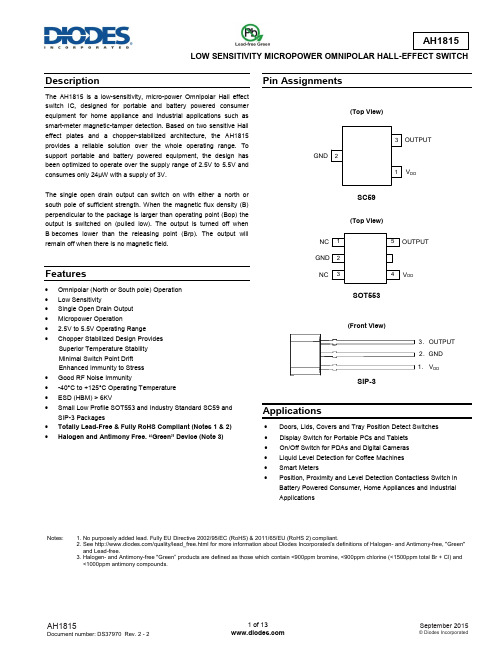
LOW SENSITIVITY MICROPOWER OMNIPOLAR HALL-EFFECT SWITCHDescriptionThe AH1815 is a low-sensitivity, micro-power Omnipolar Hall effect switch IC, designed for portable and battery powered consumer equipment for home appliance and industrial applications such as smart-meter magnetic-tamper detection. Based on two sensitive Hall effect plates and a chopper-stabilized architecture, the AH1815 provides a reliable solution over the whole operating range. To support portable and battery powered equipment, the design has been optimized to operate over the supply range of 2.5V to 5.5V and consumes only 24µW with a supply of 3V.The single open drain output can switch on with either a north or south pole of sufficient strength. When the magnetic flux density (B) perpendicular to the package is larger than operating point (Bop) the output is switched on (pulled low). The output is turned off when B becomes lower than the releasing point (Brp). The output will remain off when there is no magnetic field.Features∙ Omnipolar (North or South pole) Operation ∙ Low Sensitivity∙ Single Open Drain Output ∙ Micropower Operation∙ 2.5V to 5.5V Operating Range∙Chopper Stabilized Design Provides Superior Temperature Stability Minimal Switch Point Drift Enhanced Immunity to Stress ∙ Good RF Noise Immunity∙ -40°C to +125°C Operating Temperature ∙ ESD (HBM) > 6KV∙ Small Low Profile SOT553 and Industry Standard SC59 and SIP-3 Packages∙ Totally Lead-Free & Fully RoHS Compliant (Notes 1 & 2) ∙ Halogen and Antimony Free. “Green” Device (Note 3)Pin Assignments(Top View)132OUTPUTGND V DDSC59(Top View)NC OUTPUTV DDGND NCSOT553(Front View)1.V DD2.GND3.OUTPUTSIP-3Applications∙ Doors, Lids, Covers and Tray Position Detect Switches ∙ Display Switch for Portable PCs and Tablets ∙ On/Off Switch for PDAs and Digital Cameras∙ Liquid Level Detection for Coffee Machines ∙ Smart Meters∙Position, Proximity and Level Detection Contactless Switch in Battery Powered Consumer, Home Appliances and Industrial ApplicationsNotes: 1. No purposely added lead. Fully EU Directive 2002/95/EC (RoHS) & 2011/65/EU (RoHS 2) compliant.2. See /quality/lead_free.htmlfor more information about Diodes Incorporated’s definitions of Hal ogen- and Antimony-free, "Green" and Lead-free.3. Halogen- and Antimony-free "Green” products are defined as those which contain <900ppm bromine, <900ppm chlorine (<1500ppm total Br + Cl) and <1000ppm antimony compounds.Typical Applications Circuit (Note 4)CNote: 4. C IN is for power stabilization and to strengthen the noise immunity, the recommended capacitance is 10nF to 100nF.R L is the pull-up resistor, the recommended resistance is 10kΩ to 100k Ω.Pin DescriptionsPackages: SC59 and SIP-3Package: SOT553Note:5. NC is “No Connection” pin and is not connected internally. This pin can be left open or tied to ground.Functional Block DiagramNotes: 6. Stresses greater than the 'Absolute Maximum Ratings' specified above may cause permanent damage to the device. These are stress ratings only;functional operation of the device at these or any other conditions exceeding those indicated in this specification is not implied. Device reliability maybe affected by exposure to absolute maximum rating conditions for extended periods of time.7. The absolute maximum V DD of 7V is a transient stress rating and is not meant as a functional operating condition. It is not recommended to operatethe device at the absolute maximum rated conditions for any period of time.Electrical Characteristics (@T A = +25°C, V DD = 3V, unless otherwise specified.)Note: 8. When power is initially turned on, the operating V DD must be within its correct operating range (2.5V to 5.5V) to guarantee the output sampling.The output state is valid after the second operating cycle (typical 150ms).Magnetic Characteristics (Notes 9 & 10) (@T A = -40°C to +125°C, V DD = 2.5V to 5.5V, unless otherwise specified.)Notes: 9. Typical data is at T A = +25°C, V DD = 3V, and for design information only.10. Maximum and minimum parameters values over the operating temperature range are not tested in production, they are guaranteed by design, characterization and process control. The magnetic characteristics may vary with supply voltage, operating temperature and after soldering. 11. Maximum and minimum hysteresis is guaranteed by design and characterization.rps ops( Magnetic Flux Density B )opn rpnTypical Operating CharacteristicsMagnetic Operating Switch Points – Bop and BrpAverage Supply CurrentThermal Performance Characteristics(1) Package Types: SC59, SOT553 and SIP-3Ordering Information7 : Tape & ReelW : SC59Z : SOT553P : SIP-3B : Bulk (Note 13)A : Ammo Box (Note 12)Notes: 12. Ammo Box is for SIP-3 Spread Lead.13. Bulk is for SIP-3 Straight Lead.P D (mW)Power Dissipation CurveAMarking Information(1) Package Type: SC59( Top View )XX : Identification Code W : Week : A to Z : 1 to 26 week;Y : Year 0 to 9a to z : 27 to 52 week; z represents 52 and 53 week X : Internal Code(2) Package Type: SOT553( Top View )Y : Year : 0 to 9X : Internal codeXX : Identification Code W : Week : A to Z : 1~26 week;a to z : 27~52 week; z represents 52 and 53 week(3) Package Type: SIP-3Part Number (Front View)X : Internal CodeY : Year : 0 to 9WW : Week : 01~52, "52" represents 52 and 53 weekPackage Outline Dimensions (All dimensions in mm.)Please see AP02002 at /datasheets/ap02002.pdf for the latest version.(1) Package Type: SC59Min/MaxSensor LocationPlease see AP02002 at /datasheets/ap02002.pdf for the latest version.(2) Package Type: SOT553C LSURFACEMin/MaxSensor LocationPlease see AP02002 at /datasheets/ap02002.pdf for the latest version.(3) Package Type: SIP-3 (Bulk Pack)PART PART MARKING SURFACEMin/MaxSensor LocationAH1815Document number: DS37970 Rev. 2 - 211 of 13September 2015© Diodes IncorporatedPackage Outline Dimensions (cont.) (All dimensions in mm.)Please see AP02002 at /datasheets/ap02002.pdf for the latest version.(4) Package Type: SIP-3 (Ammo Pack)PART PART Min/MaxSensor LocationAH1815Document number: DS37970 Rev. 2 - 212 of 13September 2015© Diodes IncorporatedSuggested Pad LayoutPlease see AP02001 at /datasheets/ap02001.pdf for the latest version.(1) Package Type: SC59(2) Package Type: SOT553X E Y C Z XZYC1C2C2G13 of 13 September 2015 © Diodes IncorporatedAH1815Document number: DS37970 Rev. 2 - 2。
超通TC6215高电压低阈值双通道MOSFET说明书
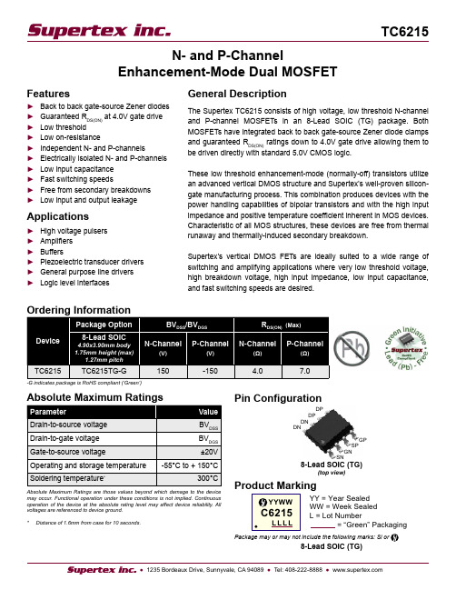
FeaturesBack to back gate-source Zener diodes Guaranteed R DS(ON) at 4.0V gate drive Low threshold Low on-resistanceIndependent N- and P-channelsElectrically isolated N- and P-channels Low input capacitance Fast switching speedsFree from secondary breakdowns Low input and output leakageApplicationsHigh voltage pulsers Amplifiers BuffersPiezoelectric transducer drivers General purpose line drivers Logic level interfaces►►►►►►►►►►►►►►►►General DescriptionThe Supertex TC6215 consists of high voltage, low threshold N-channel and P-channel MOSFETs in an 8-Lead SOIC (TG) package. Both MOSFETs have integrated back to back gate-source Zener diode clamps and guaranteed R DS(ON) ratings down to 4.0V gate drive allowing them to be driven directly with standard 5.0V CMOS logic.These low threshold enhancement-mode (normally-off) transistors utilize an advanced vertical DMOS structure and Supertex’s well-proven silicon-gate manufacturing process. This combination produces devices with the power handling capabilities of bipolar transistors and with the high input impedance and positive temperature coefficient inherent in MOS devices. Characteristic of all MOS structures, these devices are free from thermal runaway and thermally-induced secondary breakdown.Supertex’s vertical DMOS FETs are ideally suitedto a wide range of switching and amplifying applications where very low threshold voltage, high breakdown voltage, high input impedance, low input capacitance, and fast switching speeds are desired.N- and P-ChannelEnhancement-Mode Dual MOSFET-G indicates package is RoHS compliant (‘Green’)GP SP GN SNDP DP DN DNYY = Year Sealed WW = Week Sealed L = Lot Number= “Green” Packaging 8-Lead SOIC (TG)(top view)Absolute Maximum Ratings are those values beyond which damage to the device may occur. Functional operation under these conditions is not implied. Continuous operation of the device at the absolute rating level may affect device reliability. All voltages are referenced to device ground.* Distance of 1.6mm from case for 10 seconds.8-Lead SOIC (TG)Package may or may not include the following marks: Si orPin ConfigurationN-Channel Switching Waveforms and Test CircuitVOUTPUT 10V0V0VVDDInputOutputNotes:All DC parameters 100% tested at 25°C unless otherwise stated. (Pulsed test: 300µs pulse at 2% duty cycle.)All AC parameters sample tested.1.2.DD0V -10V0V V DDInputOutputNotes:All DC parameters 100% tested at 25°C unless otherwise stated. (Pulsed test: 300µs pulse at 2% duty cycle.)All AC parameters sample tested.1.2.Block DiagramSN GN SPGPDPDPDN DN 8-Lead SOIC(top view)P-Channel Output Characteristics-4.0-3.5-3.0-2.5-2.0-1.5-1.0-0.50.0-50-45-40-35-30-25-20-15-10-5V DS (volts)I D (a m p e r e s )V =-10VV =-8V V =-7VV =-6VV =-5VV =-4VV =-3VV =-2VP-Channel Saturation Characteristics-2.2-2.0-1.8-1.6-1.4-1.2-1.0-0.8-0.6-0.4-0.20.0-10-9-8-7-6-5-4-3-2-1V DS (volts)I D (a m p e r e s )V GS =-10V V GS =-8V V GS =-6V V GS =-5VV GS =-4VV GS =-3VV GS =-2VN-Channel Output Characteristics0.00.51.01.52.02.53.03.54.04.505101520253035404550V DS (volts)I D (a m p e r e s )V GS =10V V GS =8V V GS =7VV GS =6VV GS =5VV GS =4VV GS =3VV GS =2VN-Channel Saturation Characteristics0.00.51.01.52.02.53.03.54.012345678910V DS (volts)I D (a m p e r e s )V GS =10V V GS =8V V GS =6VV GS =5VV GS =4VV GS =3VV GS =2VTypical Performance CurvesSupertex inc. does not recommend the use of its products in life support applications, and will not knowingly sell them for use in such applications unless it receives an adequate “product liability indemnification insurance agreement.” Supertex inc. does not assume responsibility for use of devices described, and limits its liability to the replacement of the devices determined defective due to workmanship. No responsibility is assumed for possible omissions and inaccuracies. Circuitry and specifications are subject to change without notice. For the latest product specifications refer to the Supertex inc. website: http//.©2008 All rights reserved. Unauthorized use or reproduction is prohibited.1235 Bordeaux Drive, Sunnyvale, CA 94089(The package drawing(s) in this data sheet may not reflect the most current specifications. For the latest package outline information go to /packaging.html .)8-Lead SOIC (Narrow Body) Package Outline (TG)4.90x3.90mm body, 1.75mm height (max), 1.27mm pitchSide ViewView A-AJEDEC Registration MS-012, Variation AA, Issue E, Sept. 2005.* This dimension is not specified in the original JEDEC drawing. The value listed is for reference only.Drawings are not to scale.Supertex Doc. #: DSPD-8SOLGTG, Version H101708.Note:This chamfer feature is optional. A Pin 1 identifier must be located in the index area indicated. The Pin 1 identifier can be: a molded mark/identifier;an embedded metal marker; or a printed indicator.1.。
MSD621中文资料
PRODUCT
D ATA
SHEET
CRYSTAL CONTROLLED OSCILLATORS
Pin 1 2 3 4 5 6
Connection Enable / Disable N/C Ground Output N/C Vcc
Dimensional Tolerance: ±.005 (.127mm)
MSD621 CLOCK SERIES
100.00 MHz
CENTER FREQUENCY
Specifications subject to change without notice. DATA SHEET #: HC201 PAGE 1 OF 2 REV: 00 DATE: 11/19/03
aCopyright 2001 Connor-Winfield all rights reserved.
CW 0701 MSD621 100.00M
MSD621
DESCRIPTION
OPERATING SPECIFICATIONS
PARAMETER Frequency Range Total Frequency Tolerance Operating Temperature Range Supply Voltage Supply Current Jitter (BW=10Hz to 20MHz) Jitter (BW=12kHz to 20MHz) SSB Phase Noise at 10Hz offset SSB Phase Noise at 100Hz offset SSB Phase Noise at 1KHz offset SSB Phase Noise at 10KHz offset SSB Phase Noise at 100KHz offset
纳达电池安全性数据表说明书
Page1of4Document No.NARA-2017-01-01MATERIAL SAFETY DATA SHEETNarada Lithium BatteriesZhejiang Narada Power Source Co.,Ltd.Telephone No.:+86-571-56975979Emergency Tel No.:+86-571-56975950C Wing,No.822Wen'er West Road,Xihu District,Hangzhou,Zhejiang,P.R.ChinaDate of Preparation:7th June.2017Section I–Product IdentificationProduct Name:Polymer Lithium Ion BatteryModel:NLP704050LT20-2P/NLC704050LT20-2P/NLC583759LT20-2P/NLP883759LT20/ NLB452938H1Nominal Voltage: 3.7VChemical System:Polymer Lithium Ion Designated for Recharge:Section II–Hazardous IngredientsIMPORTANT NOTE:The battery cell should not be opened or exposed to heat because exposure to the following ingredients contained within could be harmful under some circumstances.Chemical Name CAS No.PEL TLV Lithium cobalt oxide(LiCoO2)12190-79-3None Established None EstablishedGraphite(C)7782-42-52.5mg/m3(as dust)2.5mg/m3(as dust)Organic Solvent Mixture None Established None Established lithium hexafluorophosphate(LiPF6)21324-40-3None Established None Established Palyvynilidene difluoride(PVdF)24937-79-9None Established None EstablishedSection III–Physical DataSpecific Gravity:(H20=1):LiCoO2:4.92,Graphite:2.09~2.23Melting Point:(ºC):LiCoO2about1130℃Graphite about3625℃Appearance and Odor:LiCoO2is a black,odorless powder.C is a black,odorless powder.Organic solvent is a colorless or light yellow liquid.LiPF6is a white,crystalline and odorless powder. The information and recommendations set forth are made in good faith and believed to be accurate as of the date of preparation.Narada CORP.makes no warranty,expressed or implied,Page2of4Document No.NARA-2017-01-01 Section IV—Fire and Explosion Hazard DataExtinguishing Media:WaterFlammable Limits:Not availableSpecial Fire Fighting Procedure:In case of fire in an adjacent area,use water,CO2or drychemical extinguishers if cells are packed in their originalcontainers since the fuel of the fire is basically paperproducts.For bulk quantities of unpackaged cells,useLITH-X(Graphite Base).In this case,do not use water.Section V-Reactivity DataStability:StableConditions to Avoid:Do not heat,disassemble or over charge. Hazardous Decomposition or By-products:N/AHazardous polymerization will not occur.Section VI-Health Hazard DataRoutes of Entry:Inhalation YesSkin YesIngestion YesHealth Hazards(Acute and Chronic):These chemicals are contained in a sealed can.Risk of exposure occurs only if the battery is mechanically or electrically abused.The most likely risk is an acute exposure when the gas release vent anic solvent has slight toxicity and can irritate skin and eyes.Lithium salt is irritating to skin,eyes and mucous membranes and should be avoided. Carcinogenicity:NTP:None IARC Monograph:None OSHA Regulated:NoneMedical Conditions Generally Aggravated by Exposure:An acute exposure will not generally aggravate any medical condition.Emergency and First Aid Procedures:In case of skin contact with contents of battery,flush immediately with water.For eye contact, flush with copious amounts of water for15minutes.Do not inhale leaked material.If irritation persists,get medical help.Section VII-Precautions for Safe Handling and UseSteps to be Taken in Case Material is Released or Spilled:The preferred response is to leave the area and allow the batteries to cool and the vapors to dissipate.Avoid skin and eye contact or inhalation of vapors.Remove spilled liquid withabsorbent and incinerate.Waste Disposal Method:Dispose in accordance with appropriate regulations.Open cells should be treated as hazardous waste.The information and recommendations set forth are made in good faith and believed to be accurate as of the date of preparation.Narada CORP.makes no warranty,expressed or implied,Precautions to be Taken in Handling and Storing:Avoid mechanical or electrical abuse.Other Precautions:Batteries may explode or cause burns,if disassembled,crushed or exposed to fire or high temperatures.Do not short or install with incorrect polarity.Section VIII-Control MeasureRespiratory Protection(Specify Type):Not necessary under conditions of normal use. Ventilation:Not necessary under conditions of normal use. Protective Gloves:Not necessary under conditions of normal use. Eye Protection:Not necessary under conditions of normal use. Other Protective Clothing or Equipment:Not necessary under conditions of normal use.Section IX-Recycling and DisposalNarada encourages battery recycling.Polymer Lithium ion batteries are safe for disposal in the normal municipal waste stream since they are not defined by the federal government as hazardous waste.However,Polymer lithium ion batteries are recyclable.DO NOT INCINERATE or subject battery cells to temperatures in excess of212°F.Such treatment can cause cell rupture.Section X–TransportationNarada brand Lithium ion battery packs are of a type that is eligible for exemption from requirements for transport as Class9hazardous materials or dangerous goods under most national and international regulations.The batteries have a lithium-equivalent content of less than 1.5grams per cell and less than8.0grams per battery or battery pack,as well as a Watt-hour rating of no more than20Wh per cells and no more than100Wh per battery or battery pack.In addition,the batteries are of a type that has been demonstrated to pass each applicable test(T.1 through T.8)under the UN manual of Tests and Criteria(ST/SG/AC.10/11/Rev.4),Part III, Subsection38.3.To qualify for exemption,the batteries may be subject to certain requirements.For example,under the Dangerous Goods Regulations(58th Edition,2017)of the International Air Transport Association(IATA),exempt batteries must be transported in accordance with SectionⅡof Packing Instruction965,966,or967(depending upon whether they are shipped alone,or with or in equipment).See also,the International Maritime Dangerous Goods(IMDG)Code(2010Edition) and of the U.S.Department of Transportation(DOT)regulations at49C.F.R.§172.102.In certain limited circumstances,such as if the batteries have been damaged such that they have the potential of producing a dangerous evolution of heat,fire,or short circuit,they are forbidden from transport by air.See IATA Dangerous Goods Regulations(58th Edition,2017),General Requirements of Packaging Instructions965,966,and967.Waste lithium batteries and lithium batteries being shipped for recycling or disposal are also prohibited from air transport unless approved by the appropriate national authority of the State of origin and the State of the operator. See IATA Dangerous Goods Regulations(58th Edition,2017),General Requirements of Packaging Instructions965.The information and recommendations set forth are made in good faith and believed to be accurate as of the date of preparation.Narada CORP.makes no warranty,expressed or implied, with respect to this information and disclaims all liabilities from reliance on it.。
德力DS1813通信场强电平测量仪使用说明书

11. DS1813型通讯场强仪一般性说明1.1 简介DS1813通信场强电平测量仪,是一款轻巧、性价比很高的RF 测量仪。
它体积小,重量轻具有携带方便、操作简便、LCD 图形显示、交、直流两用电源的特点。
多种测量模式选择, 全中文操作界面。
使测量和维护工作达到一个新的境界。
它广泛应用于设备测试、安装和维护移动通信设备、寻呼机行业、无绳电话、无线广播和无线电频谱监测、公安电台侦测等领域。
是RF 专业人员的必备仪器。
DS1813通信场强电平测量仪是由德力集团天津德威电子有限公司的工厂按照ISO9001国际质量管理体系标准的严格要求生产的,德威公司的ISO9001质量体系是于1996 年通过了国际认证得到注册认可的。
1.2 熟悉本机1.2.1 (1) (2) (3) 背景光开关 (4) 数值递减键 (5) 数值递增键 (6) 屏幕软键 1 (7) 屏幕软键 2 (8) 屏幕软键 3 (9) 接收模式选择(10) 数字键1(11) 数字键2(12) 数字键3(13) 数字键4(14) 数字键5(15) 数字键6(16) 数字键7(17) 数字键8(18) 数字键9(19) 数字键0(20) 小数点(21) 旋轮带背光液晶显示器面板键盘旋轮充电插口串行口射频输入口21.2.2 屏幕描述时间显示区功能指示区正文区屏幕软键F 1 软键F 2 软键 F332. DS1813型通讯场强仪快速操作指南2.1 单频率电平测量开机进入进入单频率电平测量,测量数据将如下图所示(1) 改变测量频率1) 按下软键F3使<频率>置为反显后,按动快增、快减键或转动旋轮将按照步进频率值改变频率。
2) 按动数字键输入测量频率后按下软键 F1 <确认>后可改变测量频率。
(2) 改变接收模式按动模式键将顺序改变接收模式。
其顺序是FM(窄带调频)、WFM(宽带调频)、LSB(下边带)、USB(上边带)、AM(调幅)、CW(等幅电报)、FM ... ...(3) 改变音量大小按下软键F2使<音量>置为反显后,按动快增、快减键或转动旋轮可改变音量大小。
ut621规格和参数

ut621规格和参数
目录
1.产品简介
2.主要规格
3.参数详解
4.适用场景
5.总结
正文
【1.产品简介】
UT621 是一款性能卓越的电子设备,其具备高精度、高稳定性的特点,广泛应用于各种测量和检测领域。
本文将为您详细介绍 UT621 的规格和参数,帮助您更好地了解这款产品。
【2.主要规格】
UT621 的主要规格如下:
- 尺寸:长 100mm,宽 60mm,高 40mm
- 重量:0.5kg
- 工作温度:0-50℃
- 存储温度:-20-70℃
- 电源:DC 5V
【3.参数详解】
UT621 的参数详解如下:
- 处理器:高速双核处理器,性能强劲,能够快速处理各种复杂任务
- 内存:1GB RAM,可存储大量数据,保证设备运行流畅
- 存储:16GB Flash 存储,支持扩展,方便数据备份和传输
- 显示屏:7 英寸高清触摸屏,显示效果清晰,操作便捷
- 通讯接口:支持蓝牙、Wi-Fi、以太网等多种通讯方式,方便与其他设备连接
- 传感器:内置多种传感器,如温度传感器、湿度传感器、压力传感器等,可满足多种测量需求
【4.适用场景】
UT621 适用于各种测量和检测领域,如工业生产、实验室研究、环境监测等。
凭借其出色的性能和丰富的功能,UT621 可为用户提供高效、准确的数据支持。
【5.总结】
UT621 作为一款高性能的电子设备,凭借其出色的规格和参数,在测量和检测领域具有广泛的应用前景。
无论从尺寸、重量、工作温度、电源等方面,还是从处理器、内存、存储、显示屏、通讯接口、传感器等方面,UT621 都表现出了较高的性能和稳定性。