TPS79030DBVRG4中文资料
华汕电子 1020晶体管芯片说明书

PNP S I L I C O N T R A N S I S T O R
1020 晶体管芯片说明书
█ 芯片简介
█ 管芯示意图
芯片尺寸:4 英寸(100mm)
芯片代码:A075AJ-00
芯片厚度:240±20µm
管芯尺寸:750×750µm 2
焊位尺寸:B 极 165×170µm2;E 极 150×165µm2
集电极— 发射极饱和电压 基极— 发射极饱和电压 特征频率 共基极输出电容
最小值 典型值 最大值 单位
测试条件
-50
V IC=-100µA ,IE=0
-50
V IC=-10mA,IB=0
-5
V IE=-100µA ,IC=0
-1
µA VCB=-50V,IE=0
-1
µA VEB=-5V,IC=0
70
240
█ 电参数(Ta=25℃)CEO BVEBO ICBO IEBO hFE
VCE(sat) VBE(sat) fT Cob
符号说明 集电极— 基极击穿电压 集电极— 发射极击穿电压 发射极— 基极击穿电压 集电极— 基极截止电流 发射极— 基极截止电流 直流电流增益
电极金属:铝
背面金属:金
典型封装:2SA1020
█ 极限值(Ta=25℃)(TO-92L)
Tstg——贮存温度………………………………… -55~150℃ Tj——结温…………………………………………… 150℃ PC——集电极功率耗散( Ta=25℃)…………………900mW VCBO——集电极—基极电压……………………………-50V VCEO——集电极—发射极电压…………… ……………- 50 V VEBO —— 发射极— 基极电压…………………… ………-5 V IC——集电极电流………………………………………-2A IB——基极电流…………………………………………-0.5A
P0903BDG中文资料

SYMBOL VGS
LIMITS ±20 50 35 200 40 250 8.6 50 30 -55 to 150 275
UNITS V
TC = 25 °C TC = 100 °C
ID IDM IAR
A
L = 0.1mH L = 0.05mH TC = 25 °C TC = 100 °C
EAS EAR PD Tj, Tstg TL
NIKO-SEM
N-Channel Logic Level Enhancement Mode Field Effect Transistor
P0903BDG
TO-252 (DPAK) Lead-Free
TO-252 (DPAK) MECHANICAL DATA
mm Dimension Min. A B C D E F G 9.35 2.2 0.45 0.89 0.45 0.03 5.2 Typ. Max. 10.4 2.4 0.6 1.5 0.69 0.23 6.2 H I J K L M N Dimension Min. 0.89 6.35 5.2 0.6 0.5 3.96 4.57 Typ. Max. 2.03 6.80 5.5 1 0.9 5.18 mm
Input Capacitance Output Capacitance Reverse Transfer Capacitance Total Gate Charge
2 2
Ciss Coss Crss Qg Qgs Qgd
2
1200 1800 VGS = 0V, VDS = 15V, f = 1MHz 600 350 25 VDS = 10V, VGS = 10V, ID = 25A 15 10 6 VDS = 15V, RL = 1 ID ≅ 50A, VGS = 10V, RGEN = 24 120 40 105 16 250 90 200 nS 1000 500 50 nC pF
三端稳压7805和7905稳压原理及典型电路
三端稳压7805和7905稳压原理及典范电路之老阳三干创作2010-08-21 18:02:36| 分类:家电维修 | 标签:稳压电压tj电路输出 |字号年夜中小定阅7805外形结构电子产物中,罕见的三端稳压集成电路有正电压输出的78×× 系列和负电压输出的79××系列.顾名思义,三端IC是指这种稳压用的集成电路,只有三条引脚输出,分别是输入端、接地端和输出端.它的样子象是普通的三极管,TO- 220 的标准封装,也有9013样子的TO-92封装.用78/79系列三端稳压IC来组成稳压电源所需的外围元件极少,电路内部还有过流、过热及调整管的呵护电路,使用起来可靠、方便,而且价格廉价.该系列集成稳压IC型号中的78或79后面的数字代表该三端集成稳压电路的输出电压,如7806暗示输出电压为正6V,7909暗示输出电压为负9V.因为三端固定集成稳压电路的使用方便,电子制作中经常采纳. 注意事项在实际应用中,应在三端集成稳压电路上装置足够年夜的散热器(固然小功率的条件下不用).当稳压管温渡过高时,稳压性能将变差,甚至损坏.当制作中需要一个能输出1.5A以上电流的稳压电源,通常采纳几块三端稳压电路并联起来,使其最年夜输出电流为N个1.5A,但应用时需注意:并联使用的集成稳压电路应采纳同一厂家、同一批号的产物,以保证参数的一致.另外在输出电流上留有一定的余量,以防止个别集成稳压电路失效时招致其他电路的连锁烧毁.在78 ** 、79 ** 系列三端稳压器中最常应用的是TO-220 和TO-202 两种封装.这两种封装的图形以及引脚序号、引脚功能如附图所示.从正面看①②③引脚从左向右按顺序标注,接入电路时①脚电压高于②脚,③脚为输出位.如对78**正压系列,①脚高电位,②脚接地,;对与79**负压系列,①脚接地,②脚接负电压,输出都是③脚.如附图所示.另外,还应注意,散热片总是和接地脚相连.这样在78**系列中,散热片和②脚连接,而在79**系列中,散热片却和①脚连接. 7805应用电路7805典范应用电路图:78XX系列集成稳压器的典范应用电路如下图所示,这是一个输出正5V直流电压的稳压电源电路.IC采纳集成稳压器7805,C1、C2分别为输入端和输出端滤波电容,RL为负载电阻.当输出电流较年夜时,7805应配上散热板.下图为提高输出电压的应用电路.稳压二极管VD1串接在78XX稳压器2脚与地之间,可使输出电压Uo获得一定的提高,输出电压Uo为78XX稳压器输出电压与稳压二极管VC1稳压值之和.VD2是输出呵护二极管,一旦输出电压低于VD1稳压值时,VD2导通,将输出电流旁路,呵护7800稳压器输出级不被损坏.78XX系列集成稳压器的典范应用电路如下图所示,这是一个输出正5V直流电压的稳压电源电路.IC采纳集成稳压器7805,C1、C2分别为输入端和输出端滤波电容,RL为负载电阻.当输出电较年夜时,7805应配上散热板.下图为输出电压可在一定范围内调节的应用电路.由于R1、RP电阻网络的作用,使得输出电压被提高,提高的幅度取决于RP 与R1的比值.调节电位器RP,即可一定范围内调节输出电压.当RP=0时,输出电压Uo即是78XX稳压器输出电压;当RP逐步增年夜时,Uo也随之逐步提高.下图为扩年夜输出电流的应用电路.VT2为外接扩流率管,VT1为推动管,二者为达林顿连接.R1为偏置电阻.该电路最年夜输出电流取决于VT2的参数.7805电参数7805的输入电压范围是几多78**系列的稳压集成块的极限输入电压是36V,最低输入电压为输出电压的3-4V以上.7V的电压要想输出5V,则需要使用高压差的稳压集成块,如附图所示的型号.也可以使用3只普通的整流二极管降压,也能获得5V的较为稳定的电压,二极管的允许电流年夜于你需要的电流即可.其它电路0.33uF,0.1uF的电容是旁路电容,作用是抑制电路中可能发生的自激振荡,尽量放在管脚根部,其中引脚1的电容年夜于引脚2的电容,是为了防止1处的电容漏电时,放电速度年夜于2处(输出端)的速度,招致稳压器颠倒而损坏,二极管是为了当有强电磁干扰使“地线电平”高于输出电平,使稳压器内部晶体管反向偏置而损坏设立的,这样经可以使压差在0.7V左右而不至于损坏,R1是放电电阻,加速停电后负载端空载时放电速度,防止呈现颠倒,10uF为滤波电容.LM7805---MC7805-管脚图-参数-三端稳压集成电路-封装-引脚图-典范应用电路图(MC7805/LM7805)(参照测试电路,0°C < TJ < 125°C, IO = 500mA, VI = 10V, CI= 0.33ìF, CO= 0.1ìF, 除非另有说明)三端稳压集成电路极限参数:图1 78XX内部电路图图2 78XX参照测试电路图3 外形引脚排列图管脚图图4 纹波抑制电路图5 负载调节控制电路与79XX系列三端稳压构成的正负对称输出电压电路图图7 典范应用电路图图8 TO-220封装图片图9 D-PAK封装图LM7905中文资料-MC7905-管脚图-参数-三端稳压集成电路-封装-引脚图-典范应用电路图Electrical Characteristics 电气特性 (MC7905/LM7905)(VI = -10V, IO = 500mA, 0℃≤TJ ≤ +125℃, CI =2.2μF, CO =1μF, unless otherwise specified.)三端稳压集成电路极限参数:Operating Temperature Range工作温度范围TOPR 0 ~ +125 ℃Storage Temperature Range贮存温度范围TSTG -65 ~ +150 ℃图1 79XX内部电路图图2 外形引脚排列图管脚图图3 79XX参照测试电路及典范电路图4 输出电压图5 负载调节率曲线图6 电压差曲线图图7 静态电流曲线图图8 短路电流曲线图图9 与78XX系列三端稳压构成的正负对称输出电压应用电路图图10 TO-220封装图片------------------------------------------------------------------------------------------------------------------------------------------------------------------------------------------------------------------------------------------------------------------------------------------------------------------------------------------------------------------------------------三端稳压块7805、7905、317封装形式、外围电路及实用电路7805 7815 78xx 输出+电压xx 伏,7905 7915 79... 输出-电压xx伏.==================7805管脚图与应用原理7805管脚图与应用原理图7805典范应用电路图:下图为提高输出电压的应用电路.稳压二极管VD1串接在78XX稳压器2脚与地之间,可使输出电压Uo获得一定的提高,输出电压Uo为78XX稳压器输出电压与稳压二极管VC1稳压值之和.VD2是输出呵护二极管,一旦输出电压低于VD1稳压值时,VD2导通,将输出电流旁路,呵护7800稳压器输出级不被损坏.下图为输出电压可在一定范围内调节的应用电路.由于R1、RP电阻网络的作用,使得输出电压被提高,提高的幅度取决于RP与R1的比值.调节电位器RP,即可一定范围内调节输出电压.当RP=0时,输出电压Uo即是78XX稳压器输出电压;当RP逐步增年夜时,Uo也随之逐步提高.下图为扩年夜输出电流的应用电路.VT2为外接扩流率管,VT1为推动管,二者为达林顿连接.R1为偏置电阻.该电路最年夜输出电流取决于VT2的参数.下图为提高输入电压的应用电路.78XX稳压器的最年夜输入电压为35V(7824为40V),当输入电压高于此值时,可采纳下图所示的电路.VT、R1和 VD组成一个预稳压电路,使得加在7800稳压器输入真个电压恒定在VD的稳压值上(忽略VT的b-e结压降).Ui真个最年夜输入电压仅取决于VT的耐压.集成稳压器还可以用作恒流源.下图为78XX稳压器构成的恒流源电路,其恒定电流Io即是78XX稳压器输出电压与R1的比值.79XX系列集成压器是经常使用的固定负输出电压的三端集成稳压器,除输入电压和输出电压均为负值外,其他参数和特点与78XX系列集成稳压器相同.79XX系列集成稳压的三个引脚为:1脚为接地端,2脚为输入端,3脚为输出端.79XX系列集成稳压器的应用电路也很简单.下图所示为输出-5V直流电压的稳压电源电路,IC采纳集成稳压器7905,输出电流较年夜时应配上散热板.同时运用78XX和79XX稳压器,可以组成正、负对称输出的稳压电路.下图所示为±5V稳压电源电路,IC1采纳固定正输出集成稳压器7805,IC2采用固定负输出集成稳压器7905,VD1、VD2为呵护二极管,用以防止正或负输入电压有一路未接入时损坏集成稳压器.=====================317原理1,是美国国家半导体公司的三端可调正稳压器集成电路.2,LM117/LM317 的输出电压范围是1.2V至37V.可调整输出电压低到1.2V.保证1.5A 输出电流.典范线性调整率0.01%.典范负载调整率0.1%.80dB 纹波抑制比.3,具有输出短路、过流、过热呵护以及调整管平安工作区呵护.4,它的使用非常简单,仅需两个外接电阻来设置输出电压.另外它的线性调整率和负载调整率也比标准的固定稳压器好.5,LM117/LM317 内置有过载呵护、平安区呵护等多种呵护电路.6,通常 LM117/LM317 不需要外接电容,除非输入滤波电容到 LM117/LM317 输入真个连线超越 6 英寸(约 15 厘米).使用输出电容能改变瞬态响应.调整端使用滤波电容能获得比标准三端稳压器高的多的纹波抑制比.7,LM117/LM317能够有许多特殊的用法.比如把调整端悬浮到一个较高的电压上,可以用来调节高达数百伏的电压,只要输入输出压差不超越LM117/LM317的极限就行.固然还要防止输出端短路.还可以把调整端接到一个可编程电压上,实现可编程的电源输出.8,LM317相关参数如下:VI-O 输入-输出电压差 40 VIO 输出电流内部限制工作结温LM317 0到125功耗内部限制贮存温度 -65到150 ℃9,LM317工作原理:LM317 的输入最高电压为30多伏,输出电压1.5----32V...电流1.5A...不外在用的时候要注意功耗问题...注意散热问题.LM317有三个引脚.一个输入一个输出一个电压调节.输入引脚输入正电压,输出引脚接负载, 电压调节引脚一个引脚接电阻(200左右)在输出引脚,另一个接可调电阻(几K)接于地.输入和输出引脚对地要接滤波电容.1,2脚之间为1.25V电压基准.为保证稳压器的输出性能,R1应小于240欧姆.改变R2阻值即可调整稳压电压值.D1,D2用于呵护LM317.317 系列稳压块的型号很多:例如LM317HVH、W317L等.电子快乐喜爱者经经常使用317稳压块制作输出电压可变的稳压电源(其电路的基本形式如下图所示). 稳压电源的输出电压可用下式计算,Vo=1.25(1+R2/R1).作为稳压电源的输出电压计算公式,R1和R2的阻值是不能随意设定的.首先317稳压块的输出电压变动范围是Vo=1.25V—37V(高输出电压的317稳压块如LM317HVA、LM317HVK等,其输出电压变动范围是 Vo=1.25V—45V),所以R2/R1的比值范围只能是0—28.6.其次是317稳压块都有一个最小稳定工作电流,有的资料称为最小输出电流,也有的资料称为最小泄放电流.最小稳定工作电流的值一般为1.5mA——5mA.当317稳压块的输出电流小于其最小稳定工作电流时,317稳压块就不能正常工作.当317稳压块的输出电流年夜于其最小稳定工作电流时,317稳压块就可以输出稳定的直流电压.如果用317稳压块制作稳压电源时(如图所示),没有注意317稳压块的最小稳定工作电流,那么你制作的稳压电源可能会呈现下述不正常现象:稳压电源输出的有载电压和空载电压分歧较年夜.使317稳压块稳定工作的办法是保证:a, Vo/(R1+R2)≥1.5mA——5ma,b,R2/R1的比值范围0—28.6.从图1的电路中可以看出,317的输出电压[也就是稳压电源的输出电压)U.为两个电压之和.即A、B 两点之间的电压也就是加在R2上的电压 UR2=IR2XR2,而IR2实际上是两路电流之和,一路是经R1流向R2的电流IR1,其年夜小为UR1/R1.因UR1为恒定电压1.25V,Rl是一个固定电阻,所以IR1是一个恒定的电流.另一路是317调整端流出的电流ID,由于型号分歧(例如LM317T、LM317HVH、LM317LD 等),生产厂家分歧,其ID的值各不相同.即使同一厂家,同一批次的317,其调整端流出的电流ID也各不相同.尽管这祥.但总的来说ID的电流可是有一定例律的,即ID的平均值是50uA左右,最年夜值一般不超越100uA.而且在317稳定工作时,ID的值基本上是一个恒定的值.当由于某种原因引起ID变动相对较年夜时,317就不能稳定地工作.总而言之,IR2是IR1、ID两路恒定电流之和.UR2是由两路恒定电流IR1、ID 流经R2发生的,调节R2的阻值即可调节317的输出电压Uo(U.是恒定电压UAR与UR2之和).既然ID和IR1对换节输出电压Uo 都起到了一定的作用,而且IR1是由R1提供的,IR1的年夜小也没有任何限制.是否可以使R1的阻值趋于无穷年夜,使IR1的电流值趋向于无穷小?如果可以这样做的话,就可以去失落R1,只用可变电阻R2就可以调节317的输出电压.================================三端稳压块7805、7905、317封装形式、外围电路及实用电路三端稳压块7805、7905、317外围电路.稳压电源制作图1中电容c可去除高频干扰;图2是不采纳三端稳压器的电子滤波器图3是7905负极性,图4是不采纳稳压器的负极性电子滤波器图5是可调稳压器图6是在变压器次级线圈对地接一个0.047-0.1uF的电容,以抑制调制交流声下图是封装形式:w7800、w7900系列最高输入电压为35v;w78m00、w79m00系列为40v;w317和w337也是40v.下表是w317m、 w317主要电参数:下图是实用稳压电源电路及印板图:创作时间:二零二一年六月三十日创作时间:二零二一年六月三十日。
790D中文资料

UC = 25 V @ + 125°C, SURGE = 32 V 1.0 1.0 1.0 1.0 1.0 1.0 1.3 1.8 2.7 4.0 6.0 8.8 6 6 6 6 6 6 6 6 6 6 6 6 30 14 11 6.5 5.2 4.0 2.8 2.0 1.6 1.3 1.0 0.8
DIMENSIONS in millimeters
H 0.3 Min.
B
ø 12 Min. e
A
CASE CODE A B C D
H MAX. (mm) 7.3 10.5 10.5 10.5
A MAX. (mm) 4.7 7.3 12.3 12.3
B MAX. (mm) 4.2 4.8 7.3 12.3
UC = 6.3 V @ + 125°C, SURGE = 8 V 1.0 1.5 3.3 4.7 6.8 10.0 15.0 22.0 6 6 6 6 6 6 6 8 4.0 2.5 1.3 1.4 1.3 0.6 0.6 0.4
4.7 15.0 33.0 47.0 68.0 100.0 150.0 220.0
E ± 0.15 (mm) 2.54 5.08 10.16 10.16
Ø 0.05 (+ 10%) (mm) 0.5 0.5 0.6 0.6
PACKAGING QUANTITIES
CASE CODE A B C D *Non preferred configuration on request only Document Number 42072 Revision 26-Mar-02 REEL X/Y 1000 1000 300* 200* AMMO G/H 1000 1000 300* 200* BULK B 500 250 100 50
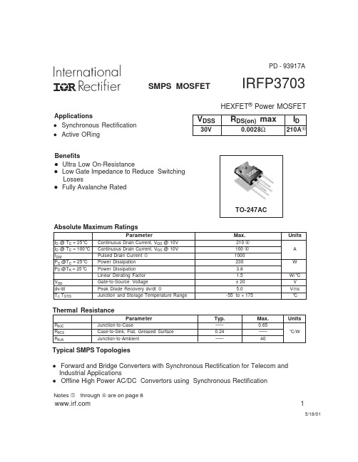
IRFP3703中文资料
Min. Typ. Max. Units ––– ––– ––– ––– ––– ––– 210 A ––– 1000 0.8 80 185 1.3 120 275 V ns nC
Conditions D MOSFET symbol showing the G integral reverse S p-n junction diode. TJ = 25°C, IS = 76A, VGS = 0V TJ = 25°C, IF = 76A, V DS = 16V di/dt = 100A/µs
元器件交易网
PD - 93917A
SMPS MOSFET
IRFP3703
HEXFET® Power MOSFET
Applications l Synchronous Rectification l Active ORing Benefits l Ultra Low On-Resistance l Low Gate Impedance to Reduce Switching Losses l Fully Avalanche Rated
Typ.
––– 0.24 –––
Max.
0.65 ––– 40
Units
°C/W
Typical SMPS Topologies
l l
Forward and Bridge Converters with Synchronous Rectification for Telecom and Industrial Applications Offline High Power AC/DC Convertors using Synchronous Rectification
Avalanche Characteristics
TS7909ACM资料

TS7900A series3-Terminal Fixed Negative Output Voltage RegulatorVoltage Range - 5V to - 24V Output Current up to 1.5AGeneral DescriptionThe TS7900A series of fixed output negative voltage regulators are intended as complements to the popular TS7800A series device. These negative regulators are available in the same seven-voltage options as the TS7800A devices.Available in fixed output voltage options from -5.0 to -24 volts, these regulators employ current limiting, thermal shutdown, and safe-area compensation--making them remarkably rugged under most operating conditions. With adequate heat sink they can deliver output currents in excess of 1.5 ampere. This series is offered in 3-pin TO-220, TO-263 package.FeaturesOutput current up to 1.5A No external components required Internal thermal overload protection Internal short-circuit current limiting Output transistor safe-area compensationOutput voltage offered in +/-2% tolerance Ordering InformationNote: Where xx denotes voltage option.Part No. Operating Temp. (Ambient) Package TS79xxACZ TO-220 TS79xxACM -20 ~ +85o CTO-263 Standard ApplicationA common ground is required between the input and the output voltages. The input voltage must remain typically 2.0Vabove the output voltage even during the low point on theInput ripple voltage.XX = these two digits of the type number indicate voltage. * = Cin is required if regulator is located an appreciabledistance from power supply filter.** = Co is not needed for stability; however, it does improve transient response.Absolute Maximum RatingInput Voltage Vin * - 35 V Input VoltageVin ** - 40 V Power Dissipation TO-220 TO-220 TO-263 Without heatsinkPt *** Without heatsink2 15 1.5 WOperating Junction Temperature Range T J 0 ~ +150 o C Storage Temperature Range T STG-65 ~ +150oCNote : * TS7905A to TS7918A ** TS7924APin assignment: 1. Ground 2. Input 3. Output(Heatsink surface connected to Pin 2)TO-263TS7905A Electrical Characteristics(Vin= -10V, Iout=500mA, 0o C ≤Tj≤125o C, Cin=0.33uF, Cout=0.1uF; unless otherwise specified.)Parameter Symbol TestConditions MinTypMaxUnitTj=25o C -4.90 -5 -5.10Output voltage Vout -7.5V≤Vin≤ -20V, 10mA≤Iout≤1A,PD≤15W-4.80 -5 -5.20 V-7.5V≤Vin≤-25V --3100Line Regulation REGline Tj=25o C-8V≤Vin≤-12V --15010mA≤Iout≤1.5A --15100Load Regulation REGload Tj=25o C250mA≤Iout≤750mA-- 5 50mVQuiescent Current Iq Iout=0, Tj=25o C --48-7.5V≤Vin≤-25V ----1.3 Quiescent Current Change ∆lq10mA≤Iout≤1A ----0.5mAOutput Noise Voltage Vn 10Hz≤f≤100KHz, Tj=25o C -- 40 -- uVRipple Rejection Ratio RR f=120Hz, -8V≤Vin≤-18V 62 74 -- dBVoltage Drop Vdrop Iout=1.0A, Tj=25o C --2--V Peak Output Current Io peak Tj=25o C -- 2.1 -- ATemperature Coefficient of Output Voltage ∆Vout/∆Tj Iout=10mA, 0o C ≤Tj≤125o C ---1--mV/o CTS7908A Electrical Characteristics(Vin=-14V, Iout=500mA, 0o C ≤Tj≤125o C, Cin=0.33uF, Cout=0.1uF; unless otherwise specified.)Parameter Symbol TestConditions MinTypMaxUnitTj=25o C -7.84 -8 -8.16Output Voltage Vout -10.5V≤Vin≤-23V,10mA≤Iout≤1A, PD≤15W-7.68 -8 -8.32 V-10.5V≤Vin≤-25V --6160Line Regulation REGline Tj=25o C-11V≤Vin≤-17V --28010mA≤Iout≤1.5A --12160Load Regulation REGload Tj=25o C250mA≤Iout≤750mA -- 4 80mVQuiescent Current Iq Iout=0, Tj=25o C --48-10.5V≤Vin≤-25V ----1 Quiescent Current Change ∆lq10mA≤Iout≤1A ----0.5mAOutput Noise Voltage Vn 10Hz≤f≤100KHz, Tj=25o C -- 52 -- uVRipple Rejection Ratio RR f=120Hz, -11V≤Vin≤-21V 5672--dB Voltage Drop Vdrop Iout=1.0A, Tj=25o C --2--V Peak Output Current Io peak Tj=25o C -- 2.1 -- ATemperature Coefficient of Output Voltage ∆Vout/∆Tj Iout10mA, 0o C ≤Tj≤125o C ---1--mV/o CPulse testing techniques are used to maintain the junction temperature as close to the ambient temperature as possible, and thermal effects must be taken into account separately.TS7909A Electrical Characteristics(Vin=-15V, Iout=500mA, 0o C ≤Tj≤125o C, Cin=0.33uF, Cout=0.1uF; unless otherwise specified.)Parameter Symbol TestConditions MinTypMaxUnitTj=25o C -8.88 -9 -9.18Output Voltage Vout -11.5V≤Vin≤-23V,10mA≤Iout≤1A, PD≤15W-8.64 -9 -9.36 V-11.5V≤Vin≤-26V --6180Line Regulation REGline Tj=25o C-12V≤Vin≤-17V --29010mA≤Iout≤1.5A --12180Load Regulation REGload Tj=25o C250mA≤Iout≤750mA -- 4 90mVQuiescent Current Iq Iout=0, Tj=25o C --48-11.5V≤Vin≤-26V ----1 Quiescent Current Change ∆lq10mA≤Iout≤1A ----0.5mAOutput Noise Voltage Vn 10Hz≤f≤100KHz, Tj=25o C -- 58 -- uVRipple Rejection Ratio RR f=120Hz, -12V≤Vin≤-22V 5671--dB Voltage Drop Vdrop Iout=1.0A, Tj=25o C --2--V Peak Output Current Io peak Tj=25o C -- 2.1 -- ATemperature Coefficient of Output Voltage ∆Vout/∆Tj Iout=10mA, 0o C ≤Tj≤125o C ---1--mV/o CTS7912A Electrical Characteristics(Vin=-19V, Iout=500mA, 0o C ≤Tj≤125o C, Cin=0.33uF, Cout=0.1uF; unless otherwise specified.)Parameter Symbol TestConditions MinTypMaxUnitTj=25o C -11.76 -12 -12.24Output Voltage Vout -14.5V≤Vin≤-27V,10mA≤Iout≤1A, PD ≤15W-11.52 -12 -12.48 V-14.5V≤Vin≤-30V --10240Line Regulation REGline Tj=25o C-15V≤Vin≤-19V --312010mA≤Iout≤1.5A --12240Load Regulation REGload Tj=25o C250mA≤Iout≤750mA -- 4 120mVQuiescent Current Iq Tj=25o C, Iout=0 -- 4 8-14.5V≤Vin≤-30V ----1 Quiescent Current Change ∆lq10mA≤Iout≤1A ----0.5mAOutput Noise Voltage Vn 10Hz≤f≤100KHz, Tj=25o C -- 75 -- uVRipple Rejection Ratio RR f=120Hz, 15V≤Vin≤25V 5570--dB Voltage Drop Vdrop Iout=1.0A, Tj=25o C --2--V Peak Output Current Io peak Tj=25o C -- 2.1 -- ATemperature Coefficient of Output Voltage ∆Vout/∆Tj Iout10mA, 0o C ≤Tj≤125o C ---1--mV/o CPulse testing techniques are used to maintain the junction temperature as close to the ambient temperature as possible, and thermal effects must be taken into account separately.TS7915A Electrical Characteristics(Vin=-23V, Iout=500mA, 0o C ≤Tj≤125o C, Cin=0.33uF, Cout=0.1uF; unless otherwise specified.)Parameter Symbol TestConditions MinTypMaxUnitTj=25o C -14.70 -15 -15.30Output Voltage Vout -17.5V≤Vin≤-30V,10mA≤Iout≤1A, PD ≤15W-14.40 -15 -15.60 V-17.5V≤Vin≤-30V --12300Line Regulation REGline Tj=25o C-18V≤Vin≤-22V --315010mA≤Iout≤1.5A --12300Load Regulation REGload Tj=25o C250mA≤Iout≤750mA -- 4 150mVQuiescent Current Iq Tj=25o C, Iout=0 -- 4 8-17.5V≤Vin≤-30V ----1 Quiescent Current Change ∆lq10mA≤Iout≤1A ----0.5mAOutput Noise Voltage Vn 10Hz≤f≤100KHz, Tj=25o C -- 90 -- uVRipple Rejection Ratio RR f=120Hz, -18V≤Vin≤-28V 5469--dB Voltage Drop Vdrop Iout=1.0A, Tj=25o C --2--V Peak Output Current Io peak Tj=25o C -- 2.1 -- ATemperature Coefficient of Output Voltage ∆Vout/∆Tj Iout=10mA, 0o C ≤Tj≤125o C ---1--mV/o CTS79818A Electrical Characteristics(Vin=-27V, Iout=500mA, 0o C ≤Tj≤125o C, Cin=0.33uF, Cout=0.1uF; unless otherwise specified.)Parameter Symbol TestConditions MinTypMaxUnitTj=25o C -17.64 -18 -18.36Output Voltage Vout -21V≤Vin≤-33V,10mA≤Iout≤1A, PD ≤15W-17.28 -18 -18.72 V-21V≤Vin≤-33V --15360Line Regulation REGline Tj=25o C-22V≤Vin≤-26V --518010mA≤Iout≤1.5A --12360Load Regulation REGload Tj=25o C250mA≤Iout≤750mA -- 4 180mVQuiescent Current Iq Tj=25o C, Iout=0 -- 4 8-21V≤Vin≤-33V ----1 Quiescent Current Change ∆lq10mA≤Iout≤1A ----0.5mAOutput Noise Voltage Vn 10Hz≤f≤100KHz, Tj=25o C --110--uV Ripple Rejection Ratio RR f=120Hz, -21V≤Vin≤-31V 5368--dB Voltage Drop Vdrop Iout=1.0A, Tj=25o C --2--V Peak Output Current Io peak Tj=25o C -- 2.1 -- ATemperature Coefficient of Output Voltage ∆Vout/∆Tj Iout10mA, 0o C ≤Tj≤125o C ---1--mV/o CPulse testing techniques are used to maintain the junction temperature as close to the ambient temperature as possible, and thermal effects must be taken into account separately.TS7824A Electrical Characteristics(Vin=-33V, Iout=500mA, 0o C ≤Tj≤125o C, Cin=0.33uF, Cout=0.1uF; unless otherwise specified.)Parameter Symbol TestConditions MinTypMaxUnitTj=25o C -23.52 -24 -24.48Output Voltage Vout -27V≤Vin≤-38V,10mA≤Iout≤1A, PD ≤15W-23.04 -24 -24.96 V-27V≤Vin≤-38V --18480Line Regulation REGline Tj=25o C-28V≤Vin≤-32V --624010mA≤Iout≤1.5A --12480Load Regulation REGload Tj=25o C250mA≤Iout≤750mA -- 4 240mVQuiescent Current Iq Iout=0, Tj=25o C --48-27V≤Vin≤-38V ----1 Quiescent Current Change ∆lq10mA≤Iout≤1A ----0.5mAOutput Noise Voltage Vn 10Hz≤f≤100KHz, Tj=25o C --170--uV Ripple Rejection Ratio RR f=120Hz, -27V≤Vin≤-37V 5065--dB Voltage Drop Vdrop Iout=1.0A, Tj=25o C --2--V Peak Output Current Io peak Tj=25o C -- 2.1 -- ATemperature Coefficient of Output Voltage ∆Vout/∆Tj Iout=10mA, 0o C ≤Tj≤125o C ---1--mV/o CPulse testing techniques are used to maintain the junction temperature as close to the ambient temperature as possible, and thermal effects must be taken into account separately.This specification applies only for DC power dissipation permitted by absolute maximum ratings.Electrical Characteristics CurveFIGURE 1 - Worst Case Power Dissipation v.s.Ambient TemperatureFIGURE 2 - Peak Output Current v.s.Input-Output Differential VoltageFIGURE 3 –Ripple Rejection v.s.FrequencyFIGURE 4 –Ripple Rejection v.s.Output VoltageFIGURE 5 –Output Voltage v.s.Junction TemperatureFIGURE 6 –Quiescent Current v.s.Temperature。
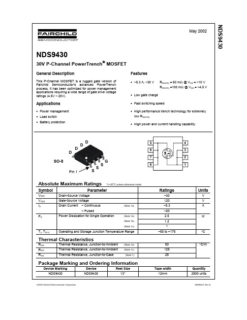
NDS9430中文资料
Reel Size 13’’
Tape width 12mm
Quantity 2500 units
NDS9430 Rev B
元器件交易网
NDS9430
Electrical Characteristics
Symbol
BVDSS ∆BVDSS ∆TJ IDSS IGSSF IGSSR VGS(th) ∆VGS(th) ∆TJ RDS(on)
元器件交易网
NDS9430
May 2002
NDh MOSFET
General Description
This P-Channel MOSFET is a rugged gate version of Fairchild Semiconductor’s advanced PowerTrench process. It has been optimized for power management applications requiring a wide range of gate drive voltage ratings (4.5V – 20V).
Features
• –5.3 A, –30 V RDS(ON) = 60 mΩ @ VGS = –10 V RDS(ON) =100 mΩ @ VGS = –4.5 V
• Low gate charge • Fast switching speed • High performance trench technology for extremely low RDS(ON) • High power and current handling capability
Typ
Max Units
V
Off Characteristics
TPS79028中文资料

SLVS299B – SEPTEMBER 2000 – REVISED MAY 2001
functional block diagram
TPS79015/18/25/28/30 IN EN 150 kΩ Vref GND Bypass Current Limit / Thermal Protection OUT
description (continued)
The TPS790xx also features a logic-enabled sleep mode to shut down the regulator, reducing quiescent current to 1 µA typical at TJ = 25°C. The TPS790xx is offered in 1.5 V, 1.8 V, 2.5 V, 2.8 V, 3.0 V.
Ground Current – µ A IO = 50 mA IO = 1 mA
15 –40 –25 –10 5 20 35 50 65 80 95 110 125 TJ – Junction Temperature – °C TPS78930
OUTPUT SPECTRAL NOISE DENSITY vs FREQUENCY
元器件交易网
TPS79015, TPS79018, TPS79025, TPS79028, TPS79030 ULTRALOW-POWER LOW-NOISE 50-mA LOW-DROPOUT LINEAR REGULATORS
SLVS299B – SEPTEMBER 2000 – REVISED MAY 2001
SLVS299B – SEPTEMBER 2000 – REVISED MAY 2001
- 1、下载文档前请自行甄别文档内容的完整性,平台不提供额外的编辑、内容补充、找答案等附加服务。
- 2、"仅部分预览"的文档,不可在线预览部分如存在完整性等问题,可反馈申请退款(可完整预览的文档不适用该条件!)。
- 3、如文档侵犯您的权益,请联系客服反馈,我们会尽快为您处理(人工客服工作时间:9:00-18:30)。
PACKAGING INFORMATIONOrderable Device Status (1)Package Type Package Drawing Pins Package Qty Eco Plan (2)Lead/Ball Finish MSL Peak Temp (3)TPS79015DBVR ACTIVE SOT-23DBV 53000Green (RoHS &no Sb/Br)CU NIPDAU Level-1-260C-UNLIM TPS79015DBVT ACTIVE SOT-23DBV 5250Green (RoHS &no Sb/Br)CU NIPDAU Level-1-260C-UNLIM TPS79018DBVR ACTIVE SOT-23DBV 53000Green (RoHS &no Sb/Br)CU NIPDAU Level-1-260C-UNLIM TPS79018DBVT ACTIVE SOT-23DBV 5250Green (RoHS &no Sb/Br)CU NIPDAU Level-1-260C-UNLIM TPS79025DBVR ACTIVE SOT-23DBV 53000Green (RoHS &no Sb/Br)CU NIPDAU Level-1-260C-UNLIM TPS79025DBVRG4ACTIVE SOT-23DBV 53000Green (RoHS &no Sb/Br)CU NIPDAU Level-1-260C-UNLIM TPS79025DBVT ACTIVE SOT-23DBV 5250Green (RoHS &no Sb/Br)CU NIPDAU Level-1-260C-UNLIM TPS79028DBVR ACTIVE SOT-23DBV 53000Green (RoHS &no Sb/Br)CU NIPDAU Level-1-260C-UNLIM TPS79028DBVT ACTIVE SOT-23DBV 5250Green (RoHS &no Sb/Br)CU NIPDAU Level-1-260C-UNLIM TPS79030DBVR ACTIVE SOT-23DBV 53000Green (RoHS &no Sb/Br)CU NIPDAU Level-1-260C-UNLIM TPS79030DBVRG4ACTIVE SOT-23DBV 53000Green (RoHS &no Sb/Br)CU NIPDAU Level-1-260C-UNLIM TPS79030DBVTACTIVESOT-23DBV5250Green (RoHS &no Sb/Br)CU NIPDAULevel-1-260C-UNLIM(1)The marketing status values are defined as follows:ACTIVE:Product device recommended for new designs.LIFEBUY:TI has announced that the device will be discontinued,and a lifetime-buy period is in effect.NRND:Not recommended for new designs.Device is in production to support existing customers,but TI does not recommend using this part in a new design.PREVIEW:Device has been announced butis not in production.Samples may or may not be available.OBSOLETE:TI has discontinued the production of the device.(2)Eco Plan -May not be currently available -please check /productcontent for the latest availability information and additional product content details.None:Not yet available Lead (Pb-Free).Pb-Free (RoHS):TI's terms "Lead-Free"or "Pb-Free"mean semiconductor products that are compatible with the current RoHS requirements for all 6substances,including the requirement that lead not exceed 0.1%by weight in homogeneous materials.Where designed to be soldered at high temperatures,TI Pb-Free products are suitable for use in specified lead-free processes.Green (RoHS &no Sb/Br):TI defines "Green"to mean "Pb-Free"and in addition,uses package materials that do not contain halogens,including bromine (Br)or antimony (Sb)above 0.1%of total product weight.(3)MSL,Peak Temp.--The Moisture Sensitivity Level rating according to the JEDECindustry standard classifications,and peak solder temperature.Important Information and Disclaimer:The information provided on this page represents TI's knowledge and belief as of the date that it is provided.TI bases its knowledge and belief on information provided by third parties,and makes no representation or warranty as to the accuracy of such information.Efforts are underway to better integrate information from third parties.TI has taken and continues to take reasonable steps to provide representative and accurate information but may not have conducted destructive testing or chemical analysis on incoming materials and chemicals.TI and TI suppliers consider certain information to be proprietary,and thus CAS numbers and other limited information may not be available for release.In no event shall TI's liability arising out of such information exceed the total purchase price of the TI part(s)at issue in this document sold by TI to Customer on an annual basis.PACKAGE OPTION ADDENDUM4-Mar-2005Addendum-Page 1IMPORTANT NOTICETexas Instruments Incorporated and its subsidiaries (TI) reserve the right to make corrections, modifications, enhancements, improvements, and other changes to its products and services at any time and to discontinue any product or service without notice. Customers should obtain the latest relevant information before placing orders and should verify that such information is current and complete. All products are sold subject to TI’s terms and conditions of sale supplied at the time of order acknowledgment.TI warrants performance of its hardware products to the specifications applicable at the time of sale in accordance with TI’s standard warranty. T esting and other quality control techniques are used to the extent TI deems necessary to support this warranty. Except where mandated by government requirements, testing of all parameters of each product is not necessarily performed.TI assumes no liability for applications assistance or customer product design. Customers are responsible for their products and applications using TI components. T o minimize the risks associated with customer products and applications, customers should provide adequate design and operating safeguards.TI does not warrant or represent that any license, either express or implied, is granted under any TI patent right, copyright, mask work right, or other TI intellectual property right relating to any combination, machine, or process in which TI products or services are used. Information published by TI regarding third-party products or services does not constitute a license from TI to use such products or services or a warranty or endorsement thereof. Use of such information may require a license from a third party under the patents or other intellectual property of the third party, or a license from TI under the patents or other intellectual property of TI.Reproduction of information in TI data books or data sheets is permissible only if reproduction is without alteration and is accompanied by all associated warranties, conditions, limitations, and notices. Reproduction of this information with alteration is an unfair and deceptive business practice. TI is not responsible or liable for such altered documentation.Resale of TI products or services with statements different from or beyond the parameters stated by TI for that product or service voids all express and any implied warranties for the associated TI product or service and is an unfair and deceptive business practice. TI is not responsible or liable for any such statements. Following are URLs where you can obtain information on other Texas Instruments products and application solutions:Products ApplicationsAmplifiers Audio /audioData Converters Automotive /automotiveDSP Broadband /broadbandInterface Digital Control /digitalcontrolLogic Military /militaryPower Mgmt Optical Networking /opticalnetwork Microcontrollers Security /securityTelephony /telephonyVideo & Imaging /videoWireless /wirelessMailing Address:Texas InstrumentsPost Office Box 655303 Dallas, Texas 75265Copyright 2005, Texas Instruments Incorporated。