HSMS-2825-TR2G中文资料
ic芯片大全
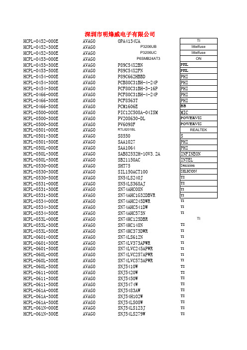
HCPL-0452-000E AVAGOHCPL-0452-300E AVAGOHCPL-0452-500E AVAGOHCPL-0453-000E AVAGOHCPL-0453-300E AVAGOHCPL-0453-500E AVAGOHCPL-0454-000E AVAGOHCPL-0454-300E AVAGOHCPL-0454-500E AVAGOHCPL-0466-000E AVAGOHCPL-0466-300E AVAGOHCPL-0466-500E AVAGOHCPL-0500-000E AVAGOHCPL-0500-300E AVAGOHCPL-0500-500E AVAGOHCPL-0501-000E AVAGOHCPL-0501-300E AVAGOHCPL-0501-500E AVAGOHCPL-050L-000E AVAGOHCPL-050L-300E AVAGOHCPL-050L-500E AVAGOHCPL-0530-000E AVAGOHCPL-0530-300E AVAGOHCPL-0530-500E AVAGOHCPL-0531-000E AVAGOHCPL-0531-300E AVAGOHCPL-0531-500E AVAGOHCPL-0534-000E AVAGOHCPL-0534-300E AVAGO SN74AHC541DW TIHCPL-0534-500E AVAGO SN74AHC573N TIHCPL-053L-000E AVAGO SN74HC125DBR TIHCPL-053L-300E AVAGO SN74HC148N TIHCPL-053L-500E AVAGO SN74HC373DWR TIHCPL-0601-000E AVAGO SN74LS612N TIHCPL-0601-300E AVAGO SN74LV373APWR TIHCPL-0601-500E AVAGO SN74LVC245APWR TIHCPL-060L-000E AVAGO SN74LVC257APWR TIHCPL-060L-300E AVAGO SN74LVC573APWR TIHCPL-060L-500E AVAGO SNJ5410W TIHCPL-0611-000E AVAGO SNJ5420W TIHCPL-0611-300E AVAGO SNJ5450W TIHCPL-0611-500E AVAGO SNJ5474W TIHCPL-061A-000E AVAGO SNJ5483AW TIHCPL-061A-300E AVAGO SNJ54H102W TIHCPL-061A-500E AVAGO SNJ54LS08W TIHCPL-061N-000E AVAGO SNJ54LS123J TIHCPL-061N-300E AVAGO SNJ54LS279W TIHCPL-061N-500E AVAGO SNJ54LS86W TIHCPL-0630-000E AVAGO SPX1585AU-2.5SPHCPL-0630-300E AVAGO SPX1585AU-3.3SPHCPL-0630-500E AVAGO SRFIC08K40R2MOTOROLA HCPL-0631-000E AVAGO SSM2166SZ ADI HCPL-0631-300E AVAGO SSM2250RU-REEL ADI HCPL-0631-500E AVAGO SST39SF010-70-4C-NH sst HCPL-063A-000E AVAGO SST39VF010-70-4C-NHE SST HCPL-063A-300E AVAGO SST39VF800A-70-4C-EK SST HCPL-063A-500E AVAGO SST39VF800A-70-4C-EK SST HCPL-063L-000E AVAGO STAC9766T SIGMATEL HCPL-063L-300E AVAGO STC809JEUR-T STC HCPL-063L-500E AVAGO STC809LEUR-T STC HCPL-063N-000E AVAGO STC809MEUR-T STC HCPL-063N-300E AVAGO STC809REUR-T STC HCPL-063N-500E AVAGO STC809SEUR-T STC HCPL-0661-000E AVAGO STC809TEUR-T STC HCPL-0661-300E AVAGO STC810JEUR-T STC HCPL-0661-500E AVAGO STC810LEUR-T STC HCPL-0700-000E AVAGO STC810MEUR-T STC HCPL-0700-300E AVAGO STC810REUR-T STC HCPL-0700-500E AVAGO STC810SEUR-T STC HCPL-0701-000E AVAGO STC810TEUR-T STC HCPL-0701-300E AVAGO STC811JEUS-T STC HCPL-0701-500E AVAGO STC811LEUS-T STC HCPL-0708-000E AVAGO STC811MEUS-T STC HCPL-0708-300E AVAGO STC811REUS-T STC HCPL-0708-500E AVAGO STC811SEUS-T STC HCPL-070A-000E AVAGO STC811TEUS-T STC HCPL-070A-300E AVAGO STC812JEUS-T STC HCPL-070A-500E AVAGO STC812LEUS-T STC HCPL-070L-000E AVAGO STC812MEUS-T STC HCPL-070L-300E AVAGO STC812REUS-T STC HCPL-070L-500E AVAGO STC812SEUS-T STC HCPL-0710-000E AVAGO STC812TEUS-T STC HCPL-0710-300E AVAGO STM809JWX6F STHCPL-0710-500E AVAGO STM809LWX6F STHCPL-0720-000E AVAGO STM809MWX6F STHCPL-0720-300E AVAGO STM809RWX6F STHCPL-0720-500E AVAGO STM809SWX6F STHCPL-0721-000E AVAGO STM809TWX6F STHCPL-0721-300E AVAGO STM810JWX6F STHCPL-0721-500E AVAGO STM810LWX6F STHCPL-0723-000E AVAGO STM810MWX6F STHCPL-0723-300E AVAGO STM810RWX6F STHCPL-0723-500E AVAGO STM810SWX6F STHCPL-0730-000E AVAGO STM810TWX6F STHCPL-0730-300E AVAGO STM811JW16F STHCPL-0730-500E AVAGO STM811LW16F STHCPL-0731-000E AVAGO STM811MW16F STHCPL-0731-300E AVAGO STM811RW16F STHCPL-0731-500E AVAGO STM811SW16F STHCPL-0738-000E AVAGO STM811TW16F STHCPL-0738-300E AVAGO STM812JW16F STHCPL-0738-500E AVAGO STM812LW16F STHCPL-073A-000E AVAGO STM812MW16F STHCPL-073A-300E AVAGO STM812RW16F STHCPL-073A-500E AVAGO STM812SW16F STHCPL-073L-000E AVAGOHCPL-073L-300E AVAGOHCPL-073L-500E AVAGOHCPL-0900-000E AVAGOHCPL-0900-300E AVAGOHCPL-0900-500E AVAGOHCPL-090J-000E AVAGOHCPL-090J-300E AVAGOHCPL-090J-500E AVAGOHCPL-091J-000E AVAGOHCPL-091J-300E AVAGOHCPL-091J-500E AVAGOHCPL-092J-000E AVAGOHCPL-092J-300E AVAGOHCPL-092J-500E AVAGOHCPL-0930-000E AVAGOHCPL-0930-300E AVAGOHCPL-0930-500E AVAGOHCPL-0931-000E AVAGOHCPL-0931-300E AVAGOHCPL-0931-500E AVAGOHCPL-181-000E AVAGOHCPL-181-00AE AVAGO TCM810TENB713MICROCHIP HCPL-181-00BE AVAGO TCM811JERCTR MICROCHIP HCPL-181-00CE AVAGO TCM811LERCTR MICROCHIP HCPL-181-00DE AVAGO TCM811MERCTR MICROCHIP HCPL-181-060E AVAGO TCM811RERCTR MICROCHIP HCPL-181-06AE AVAGO TCM811SERCTR MICROCHIP HCPL-181-06BE AVAGO TCM811TERCTR MICROCHIP HCPL-181-06CE AVAGO TCM812JERCTR MICROCHIP HCPL-181-06DE AVAGO TCM812LERCTR MICROCHIP HCPL2200-000E AVAGO TCM812MERCTR MICROCHIP HCPL-2200-000E AVAGO TCM812RERCTR MICROCHIP HCPL2200-300E AVAGO TCM812SERCTR MICROCHIP HCPL-2200-300E AVAGO TCM812TERCTR MICROCHIP HCPL2200-500E AVAGO TD1605C wearnes HCPL-2200-500E AVAGO TFDU2201-TR1VISHAY HCPL2201-000E AVAGO TFDU2201-TR3VISHAYHCPL-2201-000E AVAGO TFDU4100-TR3VISHAY HCPL2201-300E AVAGO TFDU4100-TT3VISHAY HCPL-2201-300E AVAGO TFDU4201-TR1VISHAY HCPL2201-500E AVAGO TFDU4201-TR3VISHAY HCPL-2201-500E AVAGO TFDU4202-TR1VISHAY HCPL-2202-000E AVAGO TFDU4202-TR3VISHAY HCPL-2202-300E AVAGO TFDU4203-TR1VISHAY HCPL-2202-500E AVAGO TFDU4203-TR3VISHAY HCPL-2211-000E AVAGO TISP4350H3BJR BOURNS HCPL-2211-300E AVAGO TJA1020T PHI HCPL-2211-500E AVAGO TJA1040TD PHI HCPL2212-000E AVAGO TL062IDR TI HCPL-2212-000E AVAGO TL064IDR TI HCPL2212-300E AVAGO TL071IDR TI HCPL-2212-300E AVAGO TL072IDR TI HCPL2212-500E AVAGO TL074IDR TI HCPL-2212-500E AVAGO TL081IP TIHCPL-2219-000E AVAGO TL082IDR TI HCPL-2219-300E AVAGO TL084IDR TI HCPL-2219-500E AVAGO TL431AIDR TIHCPL2231-000E AVAGO TL431BCLP TIHCPL-2231-000E AVAGO TL431IPK TIHCPL2231-300E AVAGO TLC0820AIDWR TIHCPL-2231-300E AVAGO TLC2254CD TIHCPL2231-500E AVAGO TLC27L2IDR TI HCPL-2231-500E AVAGO TLC3702CDR TIHCPL2232-000E AVAGO TLC542IDW TIHCPL-2232-000E AVAGO TLC5615CDR TIHCPL2232-300E AVAGO TLC5615IDR TIHCPL-2232-300E AVAGO TLE2062CDR TIHCPL-2232-500E AVAGO TLE2062IDR TIHCPL-2300-000E AVAGO TLV2211CDBVR TIHCPL-2300-300E AVAGO TLV2211IDBVR TIHCPL-2300-500E AVAGO TLV2231CDBVR TIHCPL-2400-000E AVAGO TLV2451IDBVR TIHCPL-2400-300E AVAGO TLV2471CDBVR TIHCPL-2400-500E AVAGO TLV2711IDBVR TIHCPL-2430-000E AVAGO TLV27L1IDBVR TIHCPL-2430-300E AVAGO TLV431AIDR TI HCPL-2430-500E AVAGO TMP82C79M-2TOSHIBA HCPL-2502-000E AVAGO TOIM4232-TR1VISHAY HCPL-2502-300E AVAGO TPA3008D2PHPRG4TI HCPL-2502-500E AVAGO TPS61042DRBR TI HCPL-2503-000E AVAGO UC2833N TI HCPL-2503-300E AVAGO UC2846DW TIHCPL-2503-500E AVAGO UC2846N TIHCPL-2530-000E AVAGO UC3833N TI HCPL-2530-300E AVAGO UC3846DWTR TIHCPL-2530-500E AVAGO UC3846N TIHCPL-2531-000E AVAGO UCC2818AADTRG4TI HCPL-2531-300E AVAGO UCC2818ADG4TI HCPL-2531-500E AVAGO UCC2818DG4TI HCPL-2601-000E AVAGO UCC2818DTRG4TI HCPL-2601-300E AVAGO UCC2895DWR TI HCPL-2601-500E AVAGO UCC3895DWR TI HCPL-2602-000E AVAGO UPC2758T-E3NECHCPL-2602-300E AVAGO uPD6453GT101NECHCPL-2602-500E AVAGO uPD6464AGT101NECHCPL-260L-000E AVAGO W78LE516-24WINBOND HCPL-260L-300E AVAGO W78LE516P-24WINBOND HCPL-260L-500E AVAGO W78LE52P-24WINBOND HCPL-2611-000E AVAGO W89C92WINBOND HCPL-2611-300E AVAGO X1227S8I XICOR HCPL-2611-500E AVAGO X25650S8I2.5XICOR HCPL-2612-000E AVAGO XEL22MICREL HCPL-2612-300E AVAGO XEL22L MICREL HCPL-2612-500E AVAGO XEL23MICREL HCPL-261A-000E AVAGO XEL23L MICREL HCPL-261A-300E AVAGO XPC850DSLZT50BU MOTOROLA HCPL-261A-500E AVAGO XR17C158CV MOTOROLA HCPL-261N-000E AVAGO TPS62220DDCR TIHCPL-261N-300E AVAGO TPS62222DDCR TIHCPL-261N-500E AVAGO HCPL-J314-000E AVAGO HCPL-2630-000E AVAGO HCPL-J314-300E AVAGO HCPL-2630-300E AVAGO HCPL-J314-500E AVAGO HCPL-2630-500E AVAGO HCPL-7860-300E AVAGO HCPL-2631-000E AVAGO HCPL-7860-500E AVAGO HCPL-2631-300E AVAGO MGA-87563-BLKG AVAGO HCPL-2631-500E AVAGO MGA-87563-TR1G AVAGO HCPL-263A-000E AVAGO MGA-87563-TR2G AVAGO HCPL-263A-300E AVAGO HLMP-6000AVAGO HCPL-263A-500E AVAGO OP42GSZ ADI HCPL-263N-000E AVAGO TLV5620IDR TI HCPL-263N-300E AVAGO DS1306EN+T DALLAS HCPL-263N-500E AVAGO TMS320F206PZA TI HCPL-2730-000E AVAGO AD8323ARUZ-REEL ADI HCPL-2730-300E AVAGO HCPL-3101-000E AVAGO HCPL-2730-500E AVAGO HCPL-3101-300E AVAGO HCPL-2731-000E AVAGO HCPL-3101-500E AVAGO HCPL-2731-300E AVAGO DS1338Z-33+DALLAS HCPL-2731-500E AVAGO DS1817R-10+TR DALLAS HCPL-273L-000E AVAGO HSMS-2825-TR2G AVAGO HCPL-273L-300E AVAGO HSMS-2825-TR1G AVAGO HCPL-273L-500E AVAGO HSMS-282C-TR1G AVAGO HCPL-3020-000E AVAGO HSMS-282C-BLKG AVAGO HCPL-3020-300E AVAGO HSMS-282C-TR2G AVAGOHCPL-3020-500E AVAGO HSMS-2820-TR1G AVAGO HCPL-3100-000E AVAGO HSMS-2820-BLKG AVAGO HCPL-3100-300E AVAGO HSMS-2820-TR2G AVAGO HCPL-3120-000E AVAGO HSMS-282F-TR1G AVAGO HCPL-3120-300E AVAGO HSMS-282F-BLKG AVAGO HCPL-3120-500E AVAGO HSMS-282F-TR2G AVAGO HCPL-3140-000E AVAGO AD712SQ/883B ADI HCPL-3140-300E AVAGO OPA2277PA TI HCPL-3140-500E AVAGO OPA2277UA TI HCPL-314J-000E AVAGO LM2675MX-ADJ NS HCPL-314J-300E AVAGO LTC1265CS Linear HCPL-314J-500E AVAGO LTC1265IS Linear HCPL-3150-000E AVAGO HSMS-2805-TR1G AVAGO HCPL-3150-300E AVAGO HSMS-2805-TR2G AVAGO HCPL-3150-500E AVAGO HSMP-3894-TR1G AVAGO HCPL-316J-000E AVAGO HSMP-3894-TR2G AVAGO HCPL-316J-300E AVAGO AT89C4051-24PU ATMEL HCPL-316J-500E AVAGO AT89C55WD-24JU ATMEL HCPL-3180-000E AVAGO MAX487ESA+T MAXIM HCPL-3180-300E AVAGO MAX487EEPA+MAXIM HCPL-3180-500E AVAGO MSP430F149IPMR TI HCPL-3700-000E AVAGO TPS65021RHAR TI HCPL-3700-300E AVAGO SSM2211SZ ADI HCPL-3700-500E AVAGO TLC3578IDW TI HCPL-3760-000E AVAGO AD9048SQ/883B ADI HCPL-3760-300E AVAGO AD9048TQ/883B ADI HCPL-3760-500E AVAGO AT89S52-24JU ATMEL HCPL-4100-000E AVAGO XC9536XL-7VQ64C XILINX HCPL-4100-300E AVAGO XTR101BG TI HCPL-4100-500E AVAGO MSC1210Y4PAGT TI HCPL-4200-000E AVAGO MSC1210Y4PAGR TI HCPL-4200-300E AVAGO ADS1178IPAPT TI HCPL-4200-500E AVAGO ACNW3190-300E AVAGO HCPL-4502-000E AVAGO MSP430F2418TPNR TI HCPL-4502-300E AVAGO MSP430F2418TPMR TI HCPL-4502-500E AVAGO XC95288XL-7TQ144C XILINX HCPL-4503-000E AVAGO TPS5100IPWR TI HCPL-4503-300E AVAGO EPM7128AETC144-10ALTERA HCPL-4503-500E AVAGO TMS320DM6446AZWTA TI HCPL-4504-000E AVAGO TMS320DM6446ZWT TI HCPL-4504-300E AVAGO UC3906N TI HCPL-4504-500E AVAGO UC3906DW TI HCPL-4506-000E AVAGO TPS54614PWPR TI HCPL-4506-300E AVAGO HCPL-0600-500E AVAGO HCPL-4506-500E AVAGO HEDS-9701#C54AVAGO HCPL-4534-000E AVAGO TLC04CP TI HCPL-4534-300E AVAGO X9313WSZ-3T1INTERSIL HCPL-4534-500E AVAGO TMS320LF2402APGA TIHCPL-4562-000E AVAGO TMS320LF2406APZA TI HCPL-4562-300E AVAGO AD9910BSVZ ADI HCPL-4562-500E AVAGO AD9957BSVZ ADI HCPL-4661-000E AVAGO TLV320AIC33IRGZ TI HCPL-4661-300E AVAGO TLV320AIC33IZQER TI HCPL-4661-500E AVAGO TPS54616PWPR TI HCPL-4731-000E AVAGO OPA551PA TI HCPL-4731-300E AVAGO DS1813R-15+DALLAS HCPL-4731-500E AVAGO TPS7333QDR TI HCPL-7510-000E AVAGO OPA277UA TI HCPL-7510-300E AVAGO LM1877MX-9NS HCPL-7510-500E AVAGO ISO7221BDR TI HCPL-7520-000E AVAGO TL16C550CIPTR TI HCPL-7520-300E AVAGO MAX9324EUP+MAXIM HCPL-7520-500E AVAGO MAX1706EEE-T MAXIM HCPL-7560-000E AVAGO TPS75733KTTR TI HCPL-7560-300E AVAGO LM2674MX-ADJ NS HCPL-7560-500E AVAGO ADS8321EB TI HCPL-7611-000E AVAGO ADS8320EB TI HCPL-7611-300E AVAGO W29C040T-90B WINBOND HCPL-7611-500E AVAGO ISO124U TI HCPL-7710-000E AVAGO FM25L04B-GTR RAMTRON HCPL-7710-300E AVAGO TLE2084CN TI HCPL-7710-500E AVAGO TL317CDR TI HCPL-7720-000E AVAGO MAX354CPE+MAXIM HCPL-7720-300E AVAGO MAX354EPE+MAXIM HCPL-7720-500E AVAGO DEI0429-WMB DEI HCPL-7721-000E AVAGO AT91SAM7SE512-AU atmel HCPL-7721-300E AVAGO EL1881CSZ-T7INTERSIL HCPL-7721-500E AVAGO SN74ACT2440FNR TI HCPL-7723-000E AVAGO MT4LC8M8C2P-5MICRON HCPL-7723-300E AVAGOHCPL-7723-500E AVAGOHCPL-7800-000E AVAGOHCPL-7800-300E AVAGOHCPL-7800-500E AVAGOHCPL-7800A-000E AVAGOHCPL-7800A-300E AVAGOHCPL-7800A-500E AVAGOHCPL-7840-000E AVAGOHCPL-7840-300E AVAGOHCPL-7840-500E AVAGOHCPL786J-000E AVAGOHCPL-786J-000E AVAGOHCPL786J-300E AVAGOHCPL-786J-300E AVAGOHCPL786J-500E AVAGOHCPL-786J-500E AVAGOHCPL788J-000E AVAGOHCPL-788J-000E AVAGOHCPL788J-300E AVAGOHCPL-788J-300E AVAGOHCPL788J-500E AVAGOHCPL-788J-500EHCPL-817-000EHCPL-817-00AEHCPL-817-00BEHCPL-817-00CEHCPL-817-00DEHCPL-817-00LEHCPL-817-060EHCPL-817-06AEHCPL-817-06BEHCPL-817-06CEHCPL-817-06DEHCPL-817-06LEHCPL-817-300EHCPL-817-30AEHCPL-817-30BEHCPL-817-30CEHCPL-817-30DEHCPL-817-30LEHCPL-817-360EHCPL-817-36AEHCPL-817-36BEHCPL-817-36CEHCPL-817-36DEHCPL-817-36LEHCPL-817-500EHCPL-817-50AEHCPL-817-50BEHCPL-817-50CEHCPL-817-50DEHCPL-817-50LEHCPL-817-560EHCPL-817-56AEHCPL-817-56BEHCPL-817-56CEHCPL-817-56DEHCPL-817-56LEHCPL-9000-000EHCPL-9000-300EHCPL-9000-500EHCPL-902J-000EHCPL-902J-300E AVAGO TLV320AIC3204IRHBR TI HCPL-902J-500E AVAGO TLV5625CDR TIHCPL-J312-000E AVAGO TLV5625IDR TIHCPL-J312-300E AVAGO TLV320AIC3104IRHBT TIHCPL-J312-500E AVAGO TLV320AIC3104IRHBR TIHCPL-J456-000E AVAGO AT45DB041D-SU ATMEL HCPL-J456-300E AVAGO MAX6657MSA+T MAXIM HCPL-J456-500E AVAGO HCPL-J454-000E AVAGO HCPL-M453-000E AVAGO HCPL-J454-300E AVAGO HCPL-M453-300E AVAGO HCPL-J454-400E AVAGO HCPL-M453-500E AVAGO HCPL-J454-500E AVAGO HCPL-M454-000E AVAGO HCPL-J454-600E AVAGO HCPL-M454-300E AVAGO TC7660IJA MICROCHIP HCPL-M454-500E AVAGO TC7660MJA MICROCHIP HCPL-M456-000E AVAGO ADT7460ARQZ ADIHCPL-M456-300E AVAGO ADSP-21065LKCA264ADIHCPL-M456-500E AVAGO ADSP-21065LKCAZ264ADI HCPL-M600-000E AVAGO AD7859ASZ ADI HCPL-M600-300E AVAGO MJD45H11G ONHCPL-M600-500E AVAGO TPD3E001DRLR TIHCPL-M601-000E AVAGO XTR116U TIHCPL-M601-300E AVAGO DS1233-5+DALLAS HCPL-M601-500E AVAGO TRU050GALGA32.0000/16.0000V ectron HCPL-M611-000E AVAGO TRU050GACCA28.7040/14.3520V ectron HCPL-M611-300E AVAGO AD9516-3BCPZ ADI HCPL-M611-500E AVAGO REF3125AIDBZT TIHCPL-M700-000E AVAGO REF3125AIDBZR TIHCPL-M700-300E AVAGO AD8592ARMZ ADI HCPL-M700-500E AVAGO QCPL-034H-500E AVAGOHD6413079F18HIT AD9865BCPZ ADI HDMP1636A AVAGO QCPL-312H-500E AVAGO HDMP-1636A AVAGO M74VHC1G135DFT1G ONHDMP-1637A AVAGO HSMD-A100-J00J1AVAGO HDMP1638AVAGO LT1587CT LTHDMP-1638AVAGO AD827JRZ-16ADI HEDS9710-R50AVAGO HSMP-389F-BLKG AVAGO HEDS-9710-R50AVAGO HSMP-389F-TR1G AVAGO HEL22MICREL HSMP-389F-TR2G AVAGO HEL23MICREL XC3064A-7PC84C XILINX HFBR-1414Z AVAGO XC3064A-7PC84I XILINX HFBR-1414TZ AVAGO Si7703EDN-T1-E3VISHAY HFBR-1521Z AVAGO Si7703EDN-T1-GE3VISHAYT-1521Z AVAGO Si7703EDN-T1-GE3ADIT-1521ETZ AVAGO AD605ARZ ADI HFBR-1521ETZ AVAGO MACH110-15JC AMDT-1522Z AVAGO MACH210-20JC AMDT-1522ETZ AVAGO LTC4213IDDB LINEAR HFBR-1522ETZ AVAGO DS1233-15+DALLAS HFBR1522Z AVAGO LTC3412EFE LINEAR HFBR-1522Z AVAGO MAX513ESD+T MAXIMHFBR1523Z AVAGO MAX3681EAG+MAXIM HFBR-1523Z AVAGO ICS1893CKILF IDT HFBR1528Z AVAGO TMS32C6416DGLZA5E0TI HFBR-1528Z AVAGO TMS32C6416EGLZ5E0TI HFBR-1531Z AVAGO TMS32C6416EGLZ6E3TI HFBR-1531ETZ AVAGO TMS32C6416EGLZ7E3TI HFBR-2531ETZ AVAGO TMS32C6416EGLZA5E0TI 1531ETZ AVAGO TMS32C6416EGLZA6E3TI 2531ETZ AVAGO AD829JRZ ADI HFBR1532Z AVAGO MAX14830ETM+MAXIM HFBR-1532Z AVAGO MX69GL128EAXGW-90G MXIC HFBR-1532ETZ AVAGO AD7811YRUZ ADI HFBR1533Z AVAGO TPS76318DBVR TI HFBR-1533Z AVAGO ADMP421ACEZ ADI HFBR-2412TZHFBR-2412ZHFBR2416TZHFBR-2416TZHFBR-2521Z AVAGO LT1304CS8Linear R-2521Z AVAGO MAX16801BEUA+T maxim R-2521ETZ AVAGO ACPL-M61L-500E AVAGO HFBR-2521ETZ AVAGO DS26503LN+DALLAS HFBR-2522Z AVAGO MAX9205EAI+T MAXIM R-2522Z AVAGO TMP105YZCT TIR-2522ETZ AVAGO TMP105YZCR TI HFBR-2522ETZ AVAGO AD5821BCBZ ADI HFBR-2523Z AVAGO PM5347-RI PMC HFBR-2528Z AVAGO PM73121-RI PMC HFBR-2531Z AVAGO TPA4411RTJT TI HFBR-2532Z AVAGO TPA4411RTJR TI HFBR-2532ETZ AVAGO LTC1438CG-ADJ Linear HFBR-2533Z AVAGO LTC1438IG-ADJ Linear HFBR-4501Z AVAGO DS1318E+DALLAS HFBR-4503Z AVAGO TMS320DM643AGDK5TI HFBR-4506Z AVAGO ACPL-M75L-000E AVAGO HFBR-4511Z AVAGO ACPL-M75L-060E AVAGO HFBR-4513Z AVAGO ACPL-M75L-500E AVAGO HFBR-4516Z AVAGO ACPL-M75L-560E AVAGO HFBR-4525Z AVAGO ACPL-T350-000E AVAGO HFBR-4526Z AVAGO ACPL-T350-060E AVAGO HFBR-4531Z AVAGO ACPL-T350-300E AVAGO HFBR-4532Z AVAGO ACPL-T350-360E AVAGO HFBR-4533Z AVAGO ACPL-T350-500E AVAGO HFBR-4535Z AVAGO ACPL-T350-560E AVAGO HFBR-4593Z AVAGO ADXRS620BBGZ ADI HFBR-4597Z AVAGO LT1521CS8Linear HFBR-EUD100Z AVAGO LT1521CS8-3.3Linear HFBR-EUD500Z AVAGO LT1521IS8LinearHFBR-EUS100Z AVAGO LT1521IS8-3.3Linear HFBR-EUS500Z AVAGO MAX6835VXSD3+T MAXIM HFBR-RUD100Z AVAGO AD9059BRSZ ADI HFBR-RUD500Z AVAGO HFBR-4515Z AVAGO HFBR-RUS100Z AVAGO HFBR-57E0PZ AVAGO HFBR-RUS500Z AVAGO HFCT-53D5EMZ AVAGO HG88510MITEL HFCT-5611AVAGOHI1-508-5HAR LT1242CS8Linear HI1-509-5HAR LT1242IS8Linear HM628512ALFP-5日立LT1140ACSW LinearHM628512BLFP-5日立AFBR-2419TZ AVAGO HS1101HUMIREL AD7156BCPZ ADIHS6118MACONICS ADP151ACBZ-2.8ADI HSDL-3201#021AVAGO DS1805Z-010+MAXIM HSDL-3201#001AVAGO TLP285-4GB TOSHIBA HSDL-3209-021AVAGO AD421BRZ ADI HSDL-7001#100AVAGO OPA2336PA TI HSDL-7002AVAGO ADUC812BSZ ADI HSMP-3814-BLKG AVAGO STPS6045CW ST HSMP-3814-TR1G AVAGO SG-3030JF EPSON HSMP-3814-TR2G AVAGO MPC8313VRAFFB FREESCAL HSMP-3822-BLKG AVAGO MAX1617AMEE+T maxim HSMP-3822-TR1G AVAGO MCP809M3X-4.63NS HSMP-3822-TR2G AVAGO MCP809M3X-4.38NS HSMP-3823-BLKG AVAGO MCP809M3X-4.00NS HSMP-3823-TR1G AVAGO MCP809M3X-3.08NS HSMP-3823-TR2G AVAGO MCP809M3X-2.93NS HSMP-3824-BLKG AVAGO MCP809M3X-2.63NS HSMP-3824-TR1G AVAGO MCP810M3X-4.63NS HSMP-3824-TR2G AVAGO MCP810M3X-4.38NS HSMP-3832-BLKG AVAGO MCP810M3X-4.00NS HSMP-3832-TR1G AVAGO MCP810M3X-3.08NS HSMP-3832-TR2G AVAGO MCP810M3X-2.93NS HSMP-3860-BLKG AVAGO MCP810M3X-2.63NS HSMP-3860-TR1G AVAGO LT1317BCS8Linear HSMP-3860-TR2G AVAGO LT1317BIS8Linear HSMP-3862-BLKG AVAGO LTC1757A-1EMS8Linear HSMP-3862-TR1G AVAGO ACPL-K342-000E AVAGO HSMP-3862-TR2G AVAGO ACPL-K342-500E AVAGO HSMP-3880-BLKG AVAGO AFBR-57M5APZ AVAGO HSMP-3880-TR1G AVAGO CY7C144AV-25AIT CY HSMP-3880-TR2G AVAGO CY7C144AV-25ACT CY HSMP-3892-BLKG AVAGO CY7C144AV-25AXIT CY HSMP-3892-TR1G AVAGO CY7C144AV-25AXCT CY HSMP-3892-TR2G AVAGO ABA-54563-TR1G AVAGO HSMP-389L-BLKG AVAGO ABA-54563-TR2G AVAGO HSMP-389L-TR1G AVAGO ABA-54563-BLKG AVAGO HSMP-389L-TR2G AVAGO LT1138ACG LinearHSMS-2812-BLKG AVAGO LT1138AIG Linear HSMS-2812-TR1G AVAGO ISL8120IRZ INTERSIL HSMS-2812-TR2G AVAGO ISL8120CRZ INTERSIL HSMS-2817-BLKG AVAGO LTC1421IG-2.5Linear HSMS-2817-TR1G AVAGO LTC1421CG-2.5Linear HSMS-2817-TR2G AVAGO MSC1212Y5PAGT TI HSMS-282K-BLKG AVAGO MSC1212Y5PAGR TI HSMS-282K-TR1G AVAGO TPS7330QDR TI HSMS-282K-TR2G AVAGO ADP3110KRZ ADI HSMS-2850-BLKG AVAGO MAX3263CAG MAXIM HSMS-2850-TR1G AVAGO MAX1729EUB MAXIM HSMS-2850-TR2G AVAGO MAX1651CSA MAXIM HSMS-8202-BLKG AVAGO AD876JR ADI HSMS-8202-TR1G AVAGO MAX1701EEE MAXIM HSMS-8202-TR2G AVAGO Si4201-BMR silicon HT2012-PL SMAR DS12C887+DALLAS HY62256ALT1-70HY LM236DR-2.5TIHY628100BLLG-70HY DS1722U DALLAS HY628100BLLG-70I HY LM7372MRX NSHY628400ALLG-55HY MAX490ESA+T MAXIM HY628400ALLG-70HY HSMS-2822-TR1G AVAGO HY62WT08081E-DG70C HY HSMP-389C-TR1G AVAGO HY62WT08081E-DG70I HY HSMP-389C-BLKG AVAGO ICL232IPE HAR HSMP-389C-TR2G AVAGO ICS8432DY-101ICS MC33375D-3.3R2G ONICS85322AM ICS AFBR-1529Z AVAGO ICS9112M-16ICS AFBR-2529Z AVAGO IDT75K62134S200BB IDT AFBR-1629Z AVAGO ILX139K SONY HSMS-2828-TR1G AVAGO IMP560ESA IMP TPS7101QDR TIIMP809JEUR-T IMP AFBR-57R5APZ AVAGO IMP809LEUR-T IMP UC3875DWPTR TIIMP809MEUR-T IMP ASSR-1510-503E AVAGO IMP809REUR-T IMP ASSR-1510-003E AVAGO IMP809SEUR-T IMP CY7B9514V-AC CYIMP809TEUR-T IMP MAX4450EXK+T MAXIM IMP810JEUR-T IMP SN75976A1DLR TIIMP810LEUR-T IMP ADUC831BSZ ADIIMP810MEUR-T IMP LTC1348IG LINEAR IMP810REUR-T IMP MSA-2111-TR1G AVAGO IMP810SEUR-T IMP DS1621S+T DALLAS IMP810TEUR-T IMP MAX485EESA+T MAXIM IMP811JEUS-T IMP MAX9669ETI+T MAXIM IMP811LEUS-T IMP MSA-0711-TR1G AVAGO IMP811MEUS-T IMP ACPL-P480-500E AVAGO IMP811REUS-T IMP HSMS-2800-TR1G AVAGO IMP811SEUS-T IMP LTC1622IS8LINEAR IMP811TEUS-T IMP MAX2102CWI MAXIMACPL-312T-500E AVAGO X24165S-2.7T1XICOR ACPL-H342-560E AVAGO X84129SI-2.5T1XICOR ACPL-H342-500E AVAGO HCNW4502-500E AVAGO ACPL-H342-060E AVAGO HCNW4502-300E AVAGO ACPL-H342-000E AVAGO AD811ARZ-16ADI ACPL-K63L-500E AVAGO TOCP155TOSHIBA ACPL-K63L-560E AVAGO TOCP200TOSHIBA ACPL-K63L-000E AVAGO HFBR-14E4Z AVAGO AFBR-5803AQZ AVAGO HFBR-24E2Z AVAGO ASSR-4128-502E AVAGO ALM-2412-TR1G AVAGO HSMH-C680AVAGO TLV320DAC23GQER TIWS1403-TR1AVAGO CY2509ZXC-1T CYLST2825-T-SC AGILENT ACPL-312T-300E AVAGO MAX853ESA+T MAXIM MAX3814CHJ+T MAXIM。
MSA2815S中文资料
1
元器件交易网
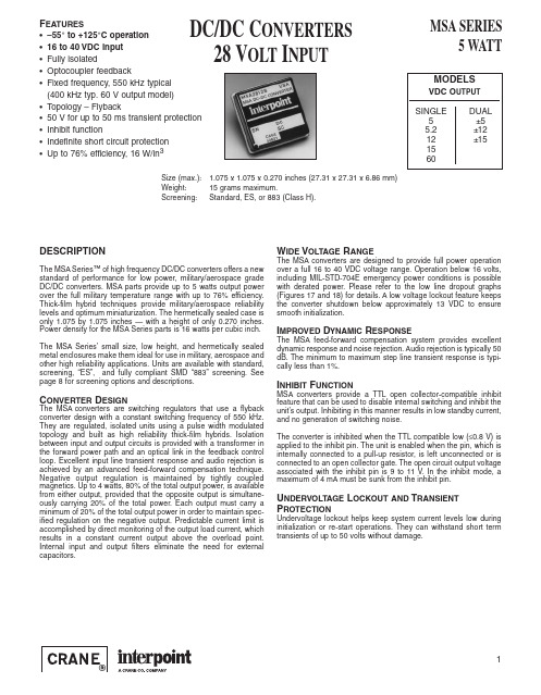
MSA SERIES
DC/DC CONVERTERS
5 WATT
ABSOLUTE MAXIMUM RATINGS
Input Voltage • 16 to 40 V
Output Power • 5 watts
Lead Soldering Temperature (10 sec per lead) • 300°C
WIDE VOLTAGE RANGE
The MSA converters are designed to provide full power operation over a full 16 to 40 VDC voltage range. Operation below 16 volts, including MIL-STD-704E emergency power conditions is possible with derated power. Please refer to the low line dropout graphs (Figures 17 and 18) for details. A low voltage lockout feature keeps the converter shutdown below approximately 13 VDC to ensure smooth initialization.
ats2825手册

ATS2825使用手册一、设备简介ATS2825是一款高效、可靠的自动测试系统,广泛应用于各种电子产品的测试和测量。
它集成了多种测试功能于一体,具有高精度、高可靠性、易操作等特点。
本手册将指导您如何正确使用ATS2825。
二、设备安装在安装ATS2825之前,请先阅读本手册并确保您已了解所有注意事项。
然后按照以下步骤进行安装:1.打开包装箱,检查设备组件是否齐全,是否有损坏。
2.根据提供的安装指南和图纸进行安装,确保将设备安装在稳定、平整的地面上。
3.连接电源和信号线,确保符合当地法规和标准。
4.进行初步测试,确保设备正常工作。
三、设备配置ATS2825的配置包括硬件和软件两部分。
请按照以下步骤进行配置:1.根据您的测试需求,选择合适的测试模块和附件,并进行连接。
2.安装随设备提供的软件,并进行必要的配置,如测试项目、测试参数等。
3.启动软件并连接ATS2825,确保软件能够控制设备进行测试。
四、设备操作ATS2825的操作主要包括软件操作和硬件操作两部分:1.软件操作:通过软件界面进行测试项目的选择、参数设置、数据采集和结果显示等操作。
2.硬件操作:根据需要连接被测件、设置测试模块、执行测试等操作。
五、设备维护为了保持ATS2825的性能和延长其使用寿命,应定期进行维护:1.清洁设备表面,保持整洁。
2.检查电源线和信号线是否连接牢固,是否有破损或腐蚀现象。
3.对测试模块进行检查和清洁,确保其正常工作。
4.对软件进行更新,以获得最新的功能和修复潜在的错误。
5.定期进行全面检查和维护,以确保设备的整体性能和可靠性。
六、常见问题与解决在遇到问题时,请参考本手册中的“常见问题与解决”部分,查找相应的问题描述和解决方案。
如果问题仍未解决,请联系制造商或专业技术人员寻求帮助。
七、技术支持与售后服务为了确保您能够充分利用ATS2825的功能并解决使用中遇到的问题,我们提供全面的技术支持和售后服务:1.技术支持:我们提供技术咨询、故障排除和技术培训等服务,以确保您正确使用设备并充分利用其功能。
HSMS-2702-TR2中文资料

元器件交易网
END VIEW
Device Orientation
For Outlines SOT-23/323
REEL
USER FEED DIRECTION
COVER TAPE
TOP VIEW 4 mm
CARRIER TAPE
END VIEW
8 mm
ABC ABC ABC ABC
Note: "AB" represents package marking code. "C" represents date code.
元器件交易网
High Performance Schottky Diode for Transient Suppression
Technical Data
HSMS-2700/ -2702 -270B / -270C
Features
• Ultra-low Series Resistance for Higher Current Handling
Tape Dimensions and Product Orientation
For Outline SOT-23
P
D
P2
E P0
F W
t1
D1
9° MAX
Ko 8° MAX
13.5° MAX
A0
B0
CAVITY
PERFORATION
HSMS-2803中文资料

Technical Data
HSMS-28XX Series
Features
• Surface Mount SOT-23/SOT143 Package
• Low Turn-On Voltage (As Low as 0.34 V at 1 mA)
HSMS-286X
7.0 0.18 0.69 10E-5 5.0 x 10E -8 1.08 5.0 0.65
2 0.5
4
IF - FORWARD CURRENT (mA)
∆VF - FORWARD VOLTAGE DIFFERENCE (mV)
IF - FORWARD CURRENT (mA)
Typical Parameters at TA = 25°C (unless otherwise noted), Single Diode
HSMS-2820 series of diodes is the best all-around choice for most applications, featuring low series resistance, low forward voltage at all current levels and good RF characteristics. The HSMS-2860 series is a high performance diode offering superior Vf and ultra-low capacitance.
CDIAGONAL = _C_1_x__C_2_ + _C_3__x_C__4 C1 + C2 C3 + C4
HS-2说明书[1]
![HS-2说明书[1]](https://img.taocdn.com/s3/m/aabb143510661ed9ad51f39c.png)
温度测量范围:-20~60℃ 湿度测量范围:0~99%RH
5.自动和手动切换通风,人工强制排风功能
系统可以切换手动和自动通风。当处于“自动测试”状态,风机只能由系统自动控制;而当处于 “手动风机”状态,可人为触摸“手动”按钮,控制风机工作。一旦人为操作情况下,工作人员已离开,系统可在半个小时后自动切换为系统“自动测试”状态。目前工作状态能在触摸显示屏上查看到。
每个分区的上行为SF6含量最高的传感器情况,下行为氧气含量最低的传感器状况,具体想了解单个区域更详细情况,可直接点击按钮菜单进入单区分布视图。
视图左上角图标 ,表示的是目前网络通信情况。右上角为目前系统时间。
2
在按钮菜单中能清楚看到当前进入的分布视图,以及目前整个系统的工作状态。
1, 表示的是多个视图之间的转换,可利用触摸屏来点击按钮进行多区领域与单区分布视图的切换。亮灯表示目前所处的区域视图。
但在断路器和gis操作过程中由于电弧电晕火花放电和局部放电高温等因素影响下sf6气体会进行分解它的分解物遇到水分后会生成腐蚀性电解质和有些高毒性分解物如sf4s2f2s2f10sof2hf和so2它们会刺激皮肤眼睛粘膜如果吸入量大还会引起头晕和肺水肿甚至致人死亡这对进入室内的检修及巡视人员的安全构成严重危险
和盛高科技产业有限公司的HS-2型SF6开关室环境监测系统主要是检测开关室环境空气中SF6气体含量和氧气含量。当环境中SF6气体含量超标或缺氧,能实时进行报警,同时自动开启通风机进行通风,并具有温、湿度检测、红外探测、工作状态语音提示、实时报警、历史数据查询等诸多功能,广泛应用于各种电压等级的SF6开关室、 组合电器室(GIS室)、SF6主变室等。
17)绝缘性能(外壳金属部分与电源之间):> 10MΩ
Precisive 5-282 自然气质量监测仪说明书

— Suitable for small-scale plants and terminals
— Ideal for remote installations
• Robust calibration — Reduced maintenance and operational
±0.05% (relative of reading)
Linearity Error
< 0.2% (relative of reading) or 0.1% (absolute), whichever is greater
Zero Drift
Not to exceed 0.2% per month
check applications
— NEMA4X, IP66, can be engine or manifold mounted
— Engineered to withstand vibration and shock
• Natural gas analysis for engine control (gas turbines, internal combustion engines, fuel cell power plants, etc.)
and Specific Gravity calculations)
* Contact MKS for higher or custom ranges
** Combustion reference/metering reference temperatures: 25°C/0°C
Precision/Repeatability
Process & Environmental Analysis Solutions
电磁流量计(上海光华)
应用 连接法兰
产品标准 安装形式
* 选择件
LDG-S电磁流量传感器
DN10~1200 1Cr18Ni9Ti 0Cr18Ni12Mo2Ti Ti Ta Hb Hc 等 聚四氟乙烯、氯丁橡胶、 聚氨酯橡胶 导电性液体(含固液二相) > 20μS/cm 0.5、1.0 0.5m/s~10m/s -25℃~+ 150℃(橡胶衬里 ≤ 80℃)
(聚氨酯衬里 ≤ 45℃) 4.0MPa~0.6MPa(按口径分) ≤0.5A 配 LDZ - 4B、4B (S) 型 ≤ 0.25A 配 LDZ - 5 型、 LDZ - 6 型 标准型 IP65(防喷水) 特殊型 IP67(防浸水)
IP68(潜水) LDZ-4B、4B(S)型 LDZ-5型 、LDZ-6型 0~10mA DC 或 4~20mA DC 1~5000Hz(配LDZ-6型)
工作压力 工作电流 防护等级
最大潜水深度 5m ≤0.5A或≤0.25A IP68(防潜水)
配套 转换器型号 输出信号
显示 通讯接口 适用电源
应用
LDZ-4B、4B(S)型 LDZ-5型 、LDZ-6型 0~10mA DC或4~20mA DC
* * 频率 (脉冲) 上限1-5000Hz (上限5000CP/S)
ISO 9001
注册证号: CCQE0800A0130
沪制00000214
LDG-/K 传感器
LDZ-4B、4B(S)型 转 换 器
中国 核工 业集团公司 上海光华 仪表 厂
目 录
1.概述 ..................................................................................................................................................................1 2.工作原理...........................................................................................................................................................1 3.性能简介...........................................................................................................................................................2 4.外形和安装尺寸................................................................................................................................................5 5.电磁流量计口径的选择.....................................................................................................................................8 6.电极材料的选择..............................................................................................................................................10 7.衬里材料的选择..............................................................................................................................................11 8.防护等级的选择..............................................................................................................................................11 9.接地环的选择..................................................................................................................................................11 10.传感器在管道上的安装..................................................................................................................................11 11. 选型编码说明................................................................................................................................................16 12.电磁流量转换器............................................................................................................................................18 13.防爆合格证...................................................................................................................................................22
- 1、下载文档前请自行甄别文档内容的完整性,平台不提供额外的编辑、内容补充、找答案等附加服务。
- 2、"仅部分预览"的文档,不可在线预览部分如存在完整性等问题,可反馈申请退款(可完整预览的文档不适用该条件!)。
- 3、如文档侵犯您的权益,请联系客服反馈,我们会尽快为您处理(人工客服工作时间:9:00-18:30)。
Surface Mount RF SchottkyBarrier DiodesTechnical DataHSMS-282x SeriesFeatures•Low Turn-On Voltage(As Low as 0.34V at 1 mA)•Low FIT (Failure in Time) Rate*•Six-sigma Quality Level •Single, Dual and QuadVersions•Unique Configurations in Surface Mount SOT-363Package– increase flexibility– save board space– reduce cost•HSMS-282K GroundedCenter Leads Provide up to10 dB Higher Isolation •Matched Diodes forConsistent Performance •Better Thermal Conductivity for Higher Power Dissipation •Lead-free Option Available *For more information see the Surface Mount SchottkyReliability Data Sheet. Description/Applications These Schottky diodes are specifically designed for both analog and digital applications. This series offers a wide range of specifications and package configurations to give the designer wide flexibility. Typical applications of these Schottky diodes are mixing, detecting, switching, sampling, clamping,Package Lead Code Identification, SOT-23/SOT-143 (Top View)COMMONCATHODECOMMONANODESERIESSINGLEPackage Lead Code Iden-tification, SOT-323(Top View)Package Lead Code Iden-tification, SOT-363(Top View)UNCONNECTEDTRIOP RHIGH ISOLATIONUNCONNECTED PAIRand wave shaping. TheHSMS-282x series of diodes is thebest all-around choice for mostapplications, featuring low seriesresistance, low forward voltage atall current levels and good RFcharacteristics.Note that Agilent’s manufacturingtechniques assure that dice foundin pairs and quads are taken fromadjacent sites on the wafer,assuring the highest degree ofmatch.2Electrical Specifications T C = 25°C, Single Diode [4]MaximumMaximum Minimum Maximum Forward Reverse Typical Part PackageBreakdown Forward Voltage Leakage Maximum Dynamic Number Marking Lead Voltage Voltage V F (V) @I R (nA) @Capacitance Resistance HSMS [5]Code Code Configuration V BR (V)V F (mV)I F (mA)V R (V)C T (pF)R D (Ω)[6]2820C0[3]0Single 153400.510100 11.0122822C2[3]2Series2823C3[3]3Common Anode 2824C4[3]4Common Cathode 2825C5[3]5Unconnected Pair 2827C7[3]7Ring Quad [5]2828C8[3]8Bridge Quad [5]2829C9[3]9Cross-over Quad 282B C0[7]B Single 282C C2[7]C Series282E C3[7]E Common Anode 282F C4[7]F Common Cathode 282K CK [7]K High IsolationUnconnected Pair 282L CL [7]L Unconnected Trio282M HH [7]M Common Cathode Quad 282N NN [7]N Common Anode Quad 282P CP [7]P Bridge Quad 282ROO [7]RRing QuadTest ConditionsI R = 100 µA I F = 1 mA [1]V F = 0 V I F = 5 mAf = 1 MHz [2]Notes:1. ∆V F for diodes in pairs and quads in 15 mV maximum at 1 mA.2. ∆C TO for diodes in pairs and quads is 0.2 pF maximum.3. Package marking code is in white.4. Effective Carrier Lifetime (τ) for all these diodes is 100 ps maximum measured with Krakauer method at 5 mA.5. See section titled “Quad Capacitance.”6. R D = R S + 5.2Ω at 25°C and I f = 5 mA.7. Package marking code is laser marked.Absolute Maximum Ratings [1] T C = 25°CSymbol Parameter Unit SOT-23/SOT-143SOT-323/SOT-363I f Forward Current (1 µs Pulse)Amp 11P IV Peak Inverse Voltage V 1515T j Junction Temperature °C 150150T stg Storage Temperature °C -65 to 150-65 to 150θjcThermal Resistance [2]°C/W500150Notes:1.Operation in excess of any one of these conditions may result in permanent damage tothe device.2.T C = +25°C, where T C is defined to be the temperature at the package pins wherecontact is made to the circuit board.1.Package marking providesorientation and identification.2.See “Electrical Specifications ” forappropriate package marking.Pin Connections and Package Marking1236543Quad CapacitanceCapacitance of Schottky diode quads is measured using an HP4271 LCR meter. Thisinstrument effectively isolates individual diode branches from the others, allowing accuratecapacitance measurement of each branch or each diode. The conditions are: 20 mV R.M.S.voltage at 1 MHz. Agilent defines this measurement as “CM ”, and it is equivalent to the capacitance of the diode by itself. The equivalent diagonal and adjacent capaci-tances can then be calculated by the formulas given below.In a quad, the diagonal capaci-tance is the capacitance between points A and B as shown in the figure below. The diagonal capacitance is calculated using the following formulaC 1 x C 2 C 3 x C 4C DIAGONAL = _______ + _______C 1 + C 2 C 3 + C 4C 1C 2C 4C 3ABCThe equivalent adjacentcapacitance is the capacitance between points A and C in the figure below. This capacitance is calculated using the following formula1C ADJACENT = C 1 + ____________1 1 1–– + –– + –– C2 C 3C 4This information does not apply to cross-over quad diodes.SPICE ParametersParameter UnitsHSMS-282x B V V 15C J0pF 0.7E G eV 0.69I BV A 1E -4I S A 2.2E-8N 1.08R S Ω 6.0P B V0.65P T 2M0.5C jR j =8.33 X 10⁻⁵ nT I b + I swhereI b = externally applied bias current in ampsI s = saturation current (see table of SPICE parameters)T = temperature, °Kn = ideality factor (see table of SPICE parameters)Note:To effectively model the packaged HSMS-282x product, please refer to Application Note AN1124.R S = series resistance (see Table of SPICE parameters)C j = junction capacitance (see Table of SPICE parameters)Linear Equivalent Circuit Model Diode ChipESD WARNING:Handling Precautions Should Be Taken To Avoid Static Discharge.4Typical Performance, T C = 25°C (unless otherwise noted), Single DiodeFigure 1. Forward Current vs. Forward Voltage at Temperatures.I F – F O R W A R D C U R R E N T (m A )V F – FORWARD VOLTAGE (V)Figure 2. Reverse Current vs. Reverse Voltage at Temperatures.I R – R E V E R S E C U R R E N T (n A )V R – REVERSE VOLTAGE (V)1100010010100,00010,000Figure 3. Total Capacitance vs. Reverse Voltage.286C T – C A P A C I T A N C E (p F )V R – REVERSE VOLTAGE (V)400.60.40.210.8Figure 4. Dynamic Resistance vs. Forward Current.0.11100R D – D Y N A M I C R E S I S T A N C E (Ω)I F – FORWARD CURRENT (mA)101101000100V F - FORWARD VOLTAGE (V)Figure 5. Typical V f Match, Series Pairs and Quads at Mixer Bias Levels.301010.3I F - F O R W A R D C U R R E N T (m A )∆V F - F O R W A R D V O L T A G E D I F F E R E N C E (m V )0.20.40.60.8 1.0 1.21.4V F - FORWARD VOLTAGE (V)Figure 6. Typical V fMatch, Series Pairs at Detector Bias Levels.100101I F - F O R W A R D C U R R E N T (µA )∆V F - F O R W A R D V O L T A G E D I F F E R E N C E (m V )0.100.150.200.25Figure 7. Typical Output Voltage vs. Input Power, Small Signal Detector Operating at 850 MHz.V O – O U T P U T V O L T A G E (V )P in – INPUT POWER (dBm)Figure 8. Typical Output Voltage vs. Input Power, Large Signal Detector Operating at 915 MHz.V O – O U T P U T V O L T A G E (V )P in – INPUT POWER (dBm)LOCAL OSCILLATOR POWER (dBm)Figure 9. Typical Conversion Loss vs. L.O. Drive, 2.0 GHz (Ref AN997).C O N V E R S I O N L O S S (d B )121098762681045Applications Information Product SelectionAgilent’s family of surface mount Schottky diodes provide unique solutions to many design prob-lems. Each is optimized for certain applications.The first step in choosing the right product is to select the diode type. All of the products in theHSMS-282x family use the same diode chip–they differ only in package configuration. The same is true of the HSMS-280x, -281x, 285x, -286x and -270x families. Each family has a different set of characteristics, which can be compared most easily by consult-ing the SPICE parameters given on each data sheet.The HSMS-282x family has been optimized for use in RF applica-tions, such asDC biased small signaldetectors to 1.5 GHz.Biased or unbiased largesignal detectors (AGC orpower monitors) to 4 GHz.Mixers and frequencymultipliers to 6 GHz.The other feature of theHSMS-282x family is itsunit-to-unit and lot-to-lot consis-tency. The silicon chip used in this series has been designed to use the fewest possible processing steps to minimize variations in diode characteristics. Statistical data on the consistency of this product, in terms of SPICE parameters, is available from Agilent.For those applications requiring very high breakdown voltage, use the HSMS-280x family of diodes. Turn to the HSMS-281x when you need very low flicker noise. TheHSMS-285x is a family of zero biasdetector diodes for small signalapplications. For high frequencydetector or mixer applications,use the HSMS-286x family. TheHSMS-270x is a series of specialtydiodes for ultra high speedclipping and clamping in digitalcircuits.Schottky Barrier Diode Char-acteristicsStripped of its package, aSchottky barrier diode chipconsists of a metal-semiconductorbarrier formed by deposition of ametal layer on a semiconductor.The most common of severaldifferent types, the passivateddiode, is shown in Figure 10,along with its equivalent circuit.R S is the parasitic series resis-tance of the diode, the sum of thebondwire and leadframe resis-tance, the resistance of the bulklayer of silicon, etc. RF energycoupled into R S is lost as heat—itdoes not contribute to the recti-fied output of the diode. C J isparasitic junction capacitance ofthe diode, controlled by the thick-ness of the epitaxial layer and thediameter of the Schottky contact.R j is the junction resistance of thediode, a function of the totalcurrent flowing through it.jCROSS-SECTION OF SCHOTTKYBARRIER DIODE CHIP CIRCUIT8.33 X 10-5n TR j = –––––––––––– = R V– R sI S + I b0.026≈––––– at 25°CI S + I bwheren =ideality factor (see table ofSPICE parameters)T =temperature in °KI S =saturation current (seetable of SPICE parameters)I b =externally applied biascurrent in ampsR v =sum of junction and seriesresistance, the slope of theV-I curveI S is a function of diode barrierheight, and can range frompicoamps for high barrier diodesto as much as 5 µA for very lowbarrier diodes.The Height of the SchottkyBarrierThe current-voltage characteristicof a Schottky barrier diode atroom temperature is described bythe following equation:V - IR SI = I S (e–––––– 1)0.026On a semi-log plot (as shown inthe Agilent catalog) the currentgraph will be a straight line withinverse slope 2.3 X 0.026 = 0.060volts per cycle (until the effect of Figure 10. Schottky Diode Chip.6R S is seen in a curve that droops at high current). All Schottky diode curves have the same slope, but not necessarily the same value of current for a given voltage. This is determined by the saturation current, I S, and is related to the barrier height of the diode.Through the choice of p-type orn-type silicon, and the selection of metal, one can tailor the characteristics of a Schottky diode. Barrier height will be altered, and at the same time C J and R S will be changed. In general, very low barrier height diodes (with high values of I S, suitable for zero bias applica-tions) are realized on p-type silicon. Such diodes suffer from higher values of R S than do then-type. Thus, p-type diodes are generally reserved for detector applications (where very high values of R V swamp out high R S) and n-type diodes such as the HSMS-282x are used for mixer applications (where high L.O. drive levels keep R V low). DC biased detectors and self-biased detectors used in gain or power control circuits.Detector Applications Detector circuits can be divided into two types, large signal(P in > -20 dBm) and small signal (P in < -20 dBm). In general, the former use resistive impedance matching at the input to improve flatness over frequency—this is possible since the input signal levels are high enough to produce adequate output voltages without the need for a high Q reactive input matching network. These circuits are self-biased (no external DC bias) and are used for gain and power control of amplifiers.Small signal detectors are used asvery low cost receivers, andrequire a reactive input imped-ance matching network toachieve adequate sensitivity andoutput voltage. Those operatingwith zero bias utilize the HSMS-285x family of detector diodes.However, superior performanceover temperature can be achievedwith the use of 3 to 30 µA of DCbias. Such circuits will use theHSMS-282x family of diodes if theoperating frequency is 1.5 GHz orlower.Typical performance of singlediode detectors (usingHSMS-2820 or HSMS-282B) canbe seen in the transfer curvesgiven in Figures 7 and 8. Suchdetectors can be realized eitheras series or shunt circuits, asshown in Figure 11.DC Biased DiodesZero Biased DiodesFigure 11. Single Diode Detec-tors.The series and shunt circuits canbe combined into a voltagedoubler[1], as shown in Figure 12.The doubler offers three advan-tages over the single diodecircuit.The two diodes are in parallelin the RF circuit, lowering theinput impedance and makingthe design of the RF matchingnetwork easier.The two diodes are in seriesin the output (video) circuit,doubling the output voltage.Some cancellation ofeven-order harmonics takesplace at the input.DC Biased DiodesZero Biased DiodesFigure 12. Voltage Doubler.The most compact and lowestcost form of the doubler isachieved when the HSMS-2822 orHSMS-282C series pair is used.Both the detection sensitivity andthe DC forward voltage of abiased Schottky detector aretemperature sensitive. Whereboth must be compensated over awide range of temperatures, thedifferential detector[2] is oftenused. Such a circuit requires thatthe detector diode and thereference diode exhibit identicalcharacteristics at all DC biaslevels and at all temperatures.This is accomplished through theuse of two diodes in one package,for example the HSMS-2825 inFigure 13. In the Agilent assemblyfacility, the two dice in a surfacemount package are taken fromadjacent sites on the wafer (asillustrated in Figure 14). This[1] Agilent Application Note 956-4, “Schottky Diode Voltage Doubler.”[2] Raymond W. Waugh, “Designing Large-Signal Detectors for Handsets and Base Stations,” Wireless Systems Design, Vol. 2, No. 7, July 1997, pp 42 – 48.7assures that the characteristics of the two diodes are more highly matched than would be possible through individual testing and hand matching.Figure 13. Differential Detector.Figure 14. Fabrication of Agilent Diode Pairs.In high power applications,coupling of RF energy from the detector diode to the reference diode can introduce error in the differential detector. TheHSMS-282K diode pair, in the six lead SOT-363 package, has a copper bar between the diodes that adds 10 dB of additional isolation between them. As this part is manufactured in theSOT-363 package it also provides the benefit of being 40% smaller than larger SOT-143 devices. The HSMS-282K is illustrated inFigure 15—note that the ground connections must be made as close to the package as possible to minimize stray inductance toground.Figure 15. High Power Differen-tial Detector.The concept of the voltage doubler can be applied to the differential detector, permitting twice the output voltage for a given input power (as well as improving input impedance and suppressing second harmonics).However, care must be taken to assure that the two reference diodes closely match the two detector diodes. One possible configuration is given in Fig-ure 16, using two HSMS-2825.Board space can be savedthrough the use of the HSMS-282P open bridge quad, as shown in Figure 17.Figure 16. Voltage DoublerDifferential Detector.Figure 17. Voltage Doubler Differential Detector.While the differential detector works well over temperature,another design approach [3] works well for large signal detectors.See Figure 18 for the schematic and a physical layout of the circuit. In this design, the two 4.7K Ω resistors and diode D2 act as a variable power divider,assuring constant output voltage over temperature and improving output linearity.Figure 18. Temperature Compen-sated Detector.In certain applications, such as a dual-band cellphone handset operating at both 900 and1800MHz, the second harmonics generated in the power control output detector when the handset is working at 900 MHz can cause problems. A filter at the output can reduce unwanted emissions at 1800 MHz in this case, but a[3] Hans Eriksson and Raymond W. Waugh, “A Temperature Compensated Linear DiodeDetector,” to be published.8lower cost solution is available [4].Illustrated schematically inFigure 19, this circuit uses diode D2 and its associated passive components to cancel all even order harmonics at the detector ’s RF input. Diodes D3 and D4provide temperature compensa-tion as described above. All four diodes are contained in a single HSMS- 282R package, as illus-trated in the layout shown in Figure 20.C1 = C2 ≈ 100 pFR1 = R2 = R3 = R4 = 4.7 K ΩD1 & D2 & D3 & D4 = HSMS-282RFigure 19. Schematic of Sup-pressed Harmonic Detector.Figure 20. Layout of Suppressed Harmonic Detector.Note that the forgoing discussion refers to the output voltage being extracted at point V+ withrespect to ground. If a differential output is taken at V+ with respect to V-, the circuit acts as a voltage doubler.Mixer applicationsThe HSMS-282x family, with its wide variety of packaging, can be used to make excellent mixers at frequencies up to 6 GHz.The HSMS-2827 ring quad of matched diodes (in the SOT-143package) has been designed for double balanced mixers. Thesmaller (SOT-363) HSMS-282R ring quad can similarly be used, if the quad is closed with externalconnections as shown in Figure 21.Figure 21. Double Balanced Mixer.Both of these networks require a crossover or a three dimensional circuit. A planar mixer can be made using the SOT-143 cross-over quad, HSMS-2829, as shown in Figure 22. In this product, a special lead frame permits the crossover to be placed inside the plastic package itself, eliminating the need for via holes (or other measures) in the RF portion of the circuit itself.Figure 22. Planar Double Bal-anced Mixer.A review of Figure 21 may lead to the question as to why theHSMS-282R ring quad is open on the ends. Distortion in double balanced mixers can be reduced if LO drive is increased, up to the point where the Schottky diodes are driven into saturation. Above this point, increased LO drive will not result in improvements in distortion. The use of expensive high barrier diodes (such as thosefabricated on GaAs) can take advantage of higher LO drive power, but a lower cost solution is to use a eight (or twelve) diode ring quad. The open design of the HSMS-282R permits this to easily be done, as shown in Figure 23.Figure 23. Low Distortion Double Balanced Mixer.This same technique can be used in the single-balanced mixer.Figure 24 shows such a mixer,with two diodes in each spot normally occupied by one. This mixer, with a sufficiently high LO drive level, will display low distortion.Figure 24. Low Distortion Bal-anced Mixer.[4] Alan Rixon and Raymond W. Waugh, “A Suppressed Harmonic Power Detector for DualBand ‘Phones,” to be published.9Sampling ApplicationsThe six lead HSMS-282P can be used in a sampling circuit, as shown in Figure 25. As was the case with the six lead HSMS-282R in the mixer, the open bridge quad is closed with traces on the circuit board. The quad was not closed internally so that it could be used in other applications, such as illustrated in Figure 17.Figure 25. Sampling Circuit. Thermal ConsiderationsThe obvious advantage of the SOT-323 and SOT-363 over the SOT-23 and SOT-142 is combina-tion of smaller size and extra leads. However, the copper leadframe in the SOT-3x3 has a thermal conductivity four times higher than the Alloy 42 leadframe of the SOT-23 and SOT-143, which enables the smaller packages to dissipate more power.The maximum junction tempera-ture for these three families of Schottky diodes is 150°C under all operating conditions. The following equation applies to the thermal analysis of diodes:Tj = (V f I f + P RF) θjc + T a (1) whereT j = junction temperatureT a = diode case temperature θjc = thermal resistanceV f I f = DC power dissipatedP RF = RF power dissipated Note that θjc, the thermal resis-tance from diode junction to thefoot of the leads, is the sum oftwo component resistances,θjc = θpkg + θchip (2)Package thermal resistance forthe SOT-3x3 package is approxi-mately 100°C/W, and the chipthermal resistance for theHSMS-282x family of diodes isapproximately 40°C/W. Thedesigner will have to add in thethermal resistance from diodecase to ambient—a poor choiceof circuit board material or heatsink design can make this numbervery high.Equation (1) would be straightfor-ward to solve but for the fact thatdiode forward voltage is a func-tion of temperature as well asforward current. The equation forV f is:11600 (V f– I f R s)nT (3)I f = I S e – 1where n = ideality factorT = temperature in °KR s = diode series resistanceand I S (diode saturation current)is given by2 1 1n– 4060(T– 298)I s = I0 (T e298 (4)Equation (4) is substituted intoequation (3), and equations (1)and (3) are solved simultaneouslyto obtain the value of junctiontemperature for given values ofdiode case temperature, DCpower dissipation and RF powerdissipation.Diode BurnoutAny Schottky junction, be it an RFdiode or the gate of a MESFET, isrelatively delicate and can beburned out with excessive RFpower. Many crystal videoreceivers used in RFID (tag)applications find themselves inpoorly controlled environmentswhere high power sources may bepresent. Examples are the areasaround airport and FAA radars,nearby ham radio operators, thevicinity of a broadcast bandtransmitter, etc. In suchenvironments, the Schottkydiodes of the receiver can beprotected by a device known as alimiter diode.[5] Formerlyavailable only in radar warningreceivers and other high costelectronic warfare applications,these diodes have been adapted tocommercial and consumercircuits.Agilent offers a complete line ofsurface mountable PIN limiterdiodes. Most notably, our HSMP-4820 (SOT-23) can act as a veryfast (nanosecond) power-sensitiveswitch when placed between theantenna and the Schottky diode,shorting out the RF circuittemporarily and reflecting theexcessive RF energy back out theantenna.[5] Agilent Application Note 1050, “LowCost, Surface Mount Power Limiters.”10Assembly InstructionsSOT-3x3 PCB FootprintRecommended PCB pad layouts for the miniature SOT-3x3 (SC-70)packages are shown in Figures 26and 27 (dimensions are in inches).These layouts provide ampleallowance for package placement by automated assembly equipment without adding parasitics that could impair the performance.Figure 26. PCB Pad Layout, SOT-323(dimensions in inches).Figure 27. PCB Pad Layout, SOT-363(dimensions in inches).Figure 28. Surface Mount Assembly Profile.SMT AssemblyReliable assembly of surface mount components is a complex process that involves manymaterial, process, and equipment factors, including: method of heating (e.g., IR or vapor phase reflow, wave soldering, etc.)circuit board material, conductor thickness and pattern, type of solder alloy, and the thermalconductivity and thermal mass of components. Components with a low mass, such as the SOTpackages, will reach solder reflow temperatures faster than those with a greater mass.Agilent ’s diodes have beenqualified to the time-temperature profile shown in Figure 28. This profile is representative of an IR reflow type of surface mount assembly process.After ramping up from room temperature, the circuit board with components attached to it (held in place with solder paste)passes through one or morepreheat zones. The preheat zones increase the temperature of the board and components to prevent thermal shock and begin evaporat-ing solvents from the solder paste.The reflow zone briefly elevates the temperature sufficiently to produce a reflow of the solder.The rates of change of tempera-ture for the ramp-up and cool-down zones are chosen to be low enough to not cause deformation of the board or damage to compo-nents due to thermal shock. The maximum temperature in the reflow zone (T MAX ) should not exceed 235°C.These parameters are typical for a surface mount assembly process for Agilent diodes. As a general guideline, the circuit board and components should be exposed only to the minimum tempera-tures and times necessary to achieve a uniform reflow of solder.TIME (seconds)T E M P E R A T U R E (°C )0501001502002506012018024030011Package DimensionsPart Number Ordering InformationNo. of Part Number Devices Container HSMS-282x-TR2*1000013" Reel HSMS-282x-TR1*30007" Reel HSMS-282x-BLK *100antistatic bagx = 0, 2, 3, 4, 5, 7, 8, 9, B, C, E, F, K, L, M, N, P or R For lead-free option, the part number will have the character "G" at the end, eg. HSMS-282x-TR2G for a 10,000 lead-free reel.Outline 23 (SOT-23)Outline 143 (SOT-143)SIDE VIEWEND VIEWDIMENSIONS ARE IN MILLIMETERS (INCHES)DIMENSIONS ARE IN MILLIMETERS (INCHES)PACKAGE MARKING CODE (XX)Outline SOT-363 (SC-70 6 Lead)Outline SOT-323 (SC-70 3 Lead)0.25 (0.010)0.15 (0.006)0.30 (0.012)0.10 (0.004)0.425 (0.017)DIMENSIONS ARE IN MILLIMETERS (INCHES)0.30 (0.012)0.10 (0.004)0.425 (0.017)DIMENSIONS ARE IN MILLIMETERS (INCHES)12Device OrientationUSER FEEDFor Outline SOT-143Note: "AB" represents package marking code. "C" represents date code.END VIEWTOP VIEW For Outlines SOT-23, -323Note: "AB" represents package marking code. "C" represents date code.END VIEWTOP VIEW END VIEWTOP VIEW Note: "AB" represents package marking code. "C" represents date code.For Outline SOT-36313Tape Dimensions and Product OrientationFor Outline SOT-23DESCRIPTIONSYMBOL SIZE (mm)SIZE (INCHES)LENGTH WIDTH DEPTH PITCHBOTTOM HOLE DIAMETER A 0B 0K 0P D 1 3.15 ± 0.102.77 ± 0.101.22 ± 0.104.00 ± 0.101.00 + 0.050.124 ± 0.0040.109 ± 0.0040.048 ± 0.0040.157 ± 0.0040.039 ± 0.002CAVITYDIAMETER PITCH POSITION D P 0E 1.50 + 0.104.00 ± 0.101.75 ± 0.100.059 + 0.0040.157 ± 0.0040.069 ± 0.004PERFORATIONWIDTH THICKNESSW t18.00 + 0.30 – 0.100.229 ± 0.0130.315 + 0.012 – 0.0040.009 ± 0.0005CARRIER TAPE CAVITY TO PERFORATION (WIDTH DIRECTION)CAVITY TO PERFORATION (LENGTH DIRECTION)F P 23.50 ± 0.052.00 ± 0.050.138 ± 0.0020.079 ± 0.002DISTANCE BETWEEN CENTERLINEFor Outline SOT-1431DESCRIPTIONSYMBOL SIZE (mm)SIZE (INCHES)LENGTH WIDTH DEPTH PITCHBOTTOM HOLE DIAMETER A 0B 0K 0P D 1 3.19 ± 0.102.80 ± 0.101.31 ± 0.104.00 ± 0.101.00 + 0.250.126 ± 0.0040.110 ± 0.0040.052 ± 0.0040.157 ± 0.0040.039 + 0.010CAVITYDIAMETER PITCH POSITION D P 0E 1.50 + 0.104.00 ± 0.101.75 ± 0.100.059 + 0.0040.157 ± 0.0040.069 ± 0.004PERFORATIONWIDTH THICKNESSW t18.00 + 0.30 – 0.100.254 ± 0.0130.315+ 0.012 – 0.0040.0100 ± 0.0005CARRIER TAPE CAVITY TO PERFORATION (WIDTH DIRECTION)CAVITY TO PERFORATION (LENGTH DIRECTION)F P 23.50 ± 0.052.00 ± 0.050.138 ± 0.0020.079 ± 0.002DISTANCE。