SB-742457_607742-69-8_DataSheet_MedChemExpress
化学发光免疫类体外诊断试剂(盒)产品技术审评要求规范(2017版)1204
化学发光免疫类体外诊断试剂(盒)产品技术审评规范(2017版)本规范旨在指导注册申请人对化学发光免疫类体外诊断试剂(盒)产品注册申报资料的准备及撰写,同时也为技术审评部门对注册申报资料的技术审评提供参考。
本规范是对化学发光免疫类体外诊断试剂(盒)产品的一般要求,申请人应依据具体产品的特性对注册申报资料的内容进行充实和细化,并依据产品特性确定其中的具体内容是否适用。
本规范是对申请人和审查人员的指导性文件,但不包括注册审批所涉及的行政事项,亦不作为法规强制执行,如果有能够满足相关法规要求的其他方法,也可以采用,但需要提供详细的研究资料和验证资料。
应在遵循相关法规的前提下使用本规范。
本规范是在现行法规和标准体系以及当前认知水平下制定的,随着法规和标准的不断完善,以及科学技术的不断发展,本规范相关内容也将进行适时调整。
一、适用范围本规范适用于利用化学发光免疫分析技术对被测物质进行定量检测的第二类体外诊断试剂(包括以微孔板、管、磁颗粒、微珠和塑料珠等为载体的酶促及非酶促化学发光免疫分析测定试剂)的注册技术审查。
依据《体外诊断试剂注册管理办法》(国家食品药品监督管理总局令第5号,以下简称《办法》)、《食品药品监管总局关于印发体外诊断试剂分类子目录的通知》(食药监械管〔2013〕242号)化学发光免疫类体外诊断试剂(盒)产品分类代号为6840。
二、注册申报资料要求(一)综述资料综述资料主要包括产品预期用途、临床意义、产品描述、有关生物安全性的说明、研究结果的总结评价以及同类产品上市情况介绍等内容,应符合《办法》和《关于公布体外诊断试剂注册申报资料要求和批准证明文件格式的公告》(国家食品药品监督管理总局公告2014年第44号)的相关要求。
(二)主要原材料研究资料(如需提供)主要原材料(例如各种天然抗原、重组抗原、单克隆抗体、多克隆抗体以及多肽类、激素类等生物原科,辣根过氧化物酶、碱性磷酸酶等标记用酶、磁微粒及其他主要原料)的选择、制备、质量标准及实验验证研究资料;校准品、质控品的原料选择、制备、赋值过程及试验资料;校准品的溯源性文件,包括具体溯源链、实验方法、数据及统计分析等详细资料。
HT-2157_DataSheet_MedChemExpress

Inhibitors, Agonists, Screening Libraries Data SheetBIOLOGICAL ACTIVITY:HT–2157 (SNAP 37889) is a selective, high–affinity, competitive antagonists of galanin–3 receptor (Gal 3).IC50 & Target: Galanin–3 receptor [1]In Vitro: HT–2157 (SNAP 37889) binds with high affinity to membranes from transiently transfected LMTK – cells expressing the human Gal 3 receptor (K i =17.44±0.01 nM; n>100) and is highly selective for Gal 3 over the Gal 1 and Gal 2 subtypes (K i >10,000 nM for each subtype; n=46 of each subtype). When tested for the antagonism of galanin–evoked inhibition of adenylyl cyclase, HT–2157 (0.1–10μM) produces concentration–dependent rightward shifts of the concentration–effect curve to galanin [1].In Vivo: The galanin–3 receptor antagonist, HT–2157 (SNAP 37889), reduces operant responding for ethanol in alcohol–preferring rats. The novel selective GALR3 antagonist, HT–2157, to reduce anxiety–like behaviour and voluntary ethanol consumption in the iP (alcohol–preferring) rat. Male iP rats treated with HT–2157 at a dose of 30 mg/kg (i.p.) do not show altered locomotor activity or changes in anxiety–like behaviour in the elevated plus maze or light–dark paradigms. Treatment with HT–2157 (30 mg/kg, i.p.)reduces operant responding for solutions containing ethanol, sucrose and saccharin. Collectively, results from the current study shows that HT–2157 (30 mg/kg, i.p.) is effective in reducing operant responding for ethanol, independent of a sedative effect [2].PROTOCOL (Extracted from published papers and Only for reference)Kinase Assay:[1]Binding affinities for HT–2157 (SNAP 37889) and SNAP 398299 at the human Gal 1, Gal 2, and Gal 3 receptors are determined by using the 125I–galanin displacement assay. Additionally, is tested for binding in a broad cross–reactivity panel that included G–protein–coupled receptors, ion channels, enzymes, and transporters. The ability of HT–2157 to antagonize functional responses to galanin is examined in modified HEK–293 cells (PEAK rapid cells) transiently cotransfected with the Gal 3 receptor and Gαz by measuring the inhibition of adenylyl cyclase activity [1].Animal Administration: HT–2157 (SNAP 37889) is prepared in 5% DMSO and 1% HMC in saline [2].[2]Rat [2]The effect of HT–2157 on locomotor activity is examined using adult male iP rats (n=12; 418–467 g). Locomotor activity is tested to ensure that any potential change in anxiety or ethanol consumption in subsequent tests is not due to any sedative property of the drug. Rats are habituated to the locomotor cells (26×26×40 cm) for 60 minute sessions which are conducted daily for threeconsecutive days. To minimise the effect of habituation during the treatment phase, rats are divided into two even groups which received a single injection of either HT–2157 (30 mg/kg, i.p.) or vehicle (1 ml/kg i.p.) 30 min prior to being placed in the locomotor cells for a 60 minute session. The following day the treatments are reversed so that all rats received treatment with both the vehicle and SNAP 37889 compound. Movements in terms of number of moves, move time (s) and total distance travelled (cm), are recorded automatically using TruScan 2.0 software.References:Product Name:HT–2157Cat. No.:HY-100717CAS No.:303149-14-6Molecular Formula:C 21H 13F 3N 2O Molecular Weight:366.34Target:Neuropeptide Y Receptor Pathway:GPCR/G Protein Solubility:DMSO: ≥ 29 mg/mL[1]. Swanson CJ, et al. Anxiolytic– and antidepressant–like profiles of the galanin–3 receptor (Gal3) antagonists SNAP 37889 and SNAP 398299. Proc Natl Acad Sci U S A. 2005 Nov 29;102(48):17489–94.[2]. Ash BL, et al. The galanin–3 receptor antagonist, SNAP 37889, reduces operant responding for ethanol in alcohol–preferring rats. Regul Pept. 2011 Jan 17;166(1–3):59–67.Caution: Product has not been fully validated for medical applications. For research use only.Tel: 609-228-6898 Fax: 609-228-5909 E-mail: tech@Address: 1 Deer Park Dr, Suite Q, Monmouth Junction, NJ 08852, USA。
体外诊断试剂的技术文件清单制定
体外诊断试剂的主要技术资料清单
序号
文件名称
可能涉及的具体
文件资料名称
内容要求(供参考)
1
产品立项
项目建议书、可行性报告等
按YY/T 0287-2003标准要求
2
设计策划
策划书
按YY/T 0287-2003标准要求
3
设计输入
设计任务书
按YY/T 0287-2003标准要求
4
风险管理文件
风险管理计划
风险分析
风险管理报告
按YY/T 0316-2003标准要求(09年6月实施YY/T 0316-2008标准)
E、校准品、质控品:质控品、标准品(校准品)的定值试验资料、溯源性等。
F、其他,如适用时的配液的PH值验证等;
4、分析性能评估资料
产品标准中规定的主要性能指标,如灵敏度、稳定性、特异性、精密度、准确度等指标的确定方法、评估资料、;
5、参考值(范围)确定资料
应详细说明确定参考值(参考范围)所采用的样本来源,说明参考值(参考范围)确定的方法,并提供参考值(参考范围)确定的详细试验资料。
2、特定产品的过程验证:(仅举几例)
A、普通化学类试剂:如适用时的冻坏过程的验证;
B、ELAIS法试剂:包被过程(最佳浓度)、酶标记的最佳浓度、终止液的终止能力等;
C、化学发光试剂:荧光物、发光底物标记的最佳浓度、PH值、终止液的终止能力等;
D、胶体金法试剂:胶体金的制备、喷涂标记(包被)过程的验证等;
74HC245DTR2G, 规格书,Datasheet 资料
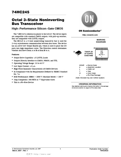
74HC245Octal 3−State Noninverting Bus TransceiverHigh −Performance Silicon −Gate CMOSThe 74HC245 is identical in pinout to the LS245. The device inputs are compatible with standard CMOS outputs; with pull −up resistors,they are compatible with LSTTL outputs.The HC245 is a 3−state noninverting transceiver that is used for 2−way asynchronous communication between data buses. The device has an active −low Output Enable pin, which is used to place the I/O ports into high −impedance states. The Direction control determines whether data flows from A to B or from B to A.Features•Output Drive Capability: 15 LSTTL Loads•Outputs Directly Interface to CMOS, NMOS, and TTL •Operating V oltage Range: 2.0 to 6.0 V •Low Input Current: 1.0 m A•High Noise Immunity Characteristic of CMOS Devices•In Compliance with the Requirements Defined by JEDEC Standard No. 7A•ESD Performance: HBM > 2000 V; Machine Model > 200 V•Chip Complexity: 308 FETs or 77 Equivalent Gates •This is a Pb −Free Device120MARKING DIAGRAMSHC 245ALYW GGTSSOP −20DT SUFFIX CASE 948ESee detailed ordering and shipping information in the package dimensions section on page 2 of this data sheet.ORDERING INFORMATIONHC245= Device CodeA = Assembly Location L = Wafer Lot Y = YearW = Work WeekG = Pb −Free Package(Note: Microdot may be in either location)Figure 1. Pin Assignment A5A3A2A1DIRECTIONGNDA8A7A6A4B3B2B1OUTPUT ENABLE V CCB8B7B6B5B4A DATA PORTA8A7A6A5A3A4A2A1DIRECTION OUTPUT ENABLEPIN 10 = GND PIN 20 = V CCB1B2B3B4B5B6B7B8B DATA PORTFigure 2. Logic DiagramFUNCTION TABLEControl Inputs OperationOutput Enable DirectionL L Data Transmitted from Bus B to Bus A L H Data Transmitted from Bus A to Bus B H XBuses Isolated (High −Impedance State)X = don’t careORDERING INFORMATIONDevicePackage Shipping †74HC245DTR2GTSSOP −20*2500 / Tape & Reel†For information on tape and reel specifications, including part orientation and tape sizes, please refer to our Tape and Reel Packaging Specifications Brochure, BRD8011/D.*This package is inherently Pb −Free.MAXIMUM RATINGS (Note 1)Symbol Parameter Value Unit V CC DC Supply Voltage*0.5 to )7.0V V IN DC Input Voltage*0.5 to V CC)0.5V V OUT DC Output Voltage(Note 2)*0.5 to V CC)0.5VI IK DC Input Diode Current$20mAI OK DC Output Diode Current$35mA I OUT DC Output Sink Current$35mAI CC DC Supply Current per Supply Pin$75mA I GND DC Ground Current per Ground Pin$75mA T STG Storage Temperature Range*65 to )150_C T L Lead Temperature, 1 mm from Case for 10 Seconds260_C T J Junction Temperature Under Bias)150_C q JA Thermal Resistance TSSOP128_C/W P D Power Dissipation in Still Air at 85_C TSSOP450mW MSL Moisture Sensitivity Level 1F R Flammability Rating Oxygen Index: 30% to 35%UL 94 V−0 @ 0.125 inV ESD ESD Withstand Voltage Human Body Model (Note 3)Machine Model (Note 4)u2000u200VI LATCHUP Latchup Performance Above V CC and Below GND at 85_C (Note 5)$300mA Stresses exceeding Maximum Ratings may damage the device. Maximum Ratings are stress ratings only. Functional operation above theRecommended Operating Conditions is not implied. Extended exposure to stresses above the Recommended Operating Conditions may affect device reliability.1.Measured with minimum pad spacing on an FR4 board, using 10 mm−by−1 inch, 20 ounce copper trace with no air flow.2.I O absolute maximum rating must observed.3.Tested to EIA/JESD22−A114−A.4.Tested to EIA/JESD22−A115−A.5.Tested to EIA/JESD78.RECOMMENDED OPERATING CONDITIONSSymbol Parameter Min Max Unit V CC DC Supply Voltage (Referenced to GND) 2.0 6.0VV in, V out DC Input Voltage, Output Voltage (Referenced to GND)0V CC V T A Operating Temperature, All Package Types–55+125_Ct r, t f Input Rise and Fall Time V CC = 2.0 V (Figure 3)V CC = 4.5 VV CC = 6.0 V 01000500400nsDC ELECTRICAL CHARACTERISTICS (Voltages Referenced to GND)Guaranteed LimitSymbol Parameter Test Conditions V CCV–55 to25_C v 85_C v 125_C UnitV IH Minimum High−Level Input Voltage V out = V CC – 0.1 V|I out| v 20 m A 2.03.04.56.01.52.13.154.21.52.13.154.21.52.13.154.2VV IL Maximum Low−Level Input Voltage V out = 0.1 V|I out| v 20 m A 2.03.04.56.00.50.91.351.80.50.91.351.80.50.91.351.8VV OH Minimum High−Level Output Voltage V in = V IH|I out| v 20 m A2.04.56.01.94.45.91.94.45.91.94.45.9VV in = V IH|I out| v 2.4 mA|I out| v 6.0 mA|I out| v 7.8 mA3.04.56.02.483.985.482.343.845.342.23.75.2V OL Maximum Low−Level Output Voltage V in = V IL|I out| v 20 m A2.04.56.00.10.10.10.10.10.10.10.10.1VV in = V IL|I out| v 2.4 mA|I out| v 6.0 mA|I out| v 7.8 mA3.04.56.00.260.260.260.330.330.330.40.40.4I in Maximum Input Leakage Current V in = V CC or GND 6.0±0.1±1.0±1.0m AI OZ Maximum Three−State LeakageCurrent Output in High−Impedance StateV in = V IL or V IHV out = V CC or GND6.0±0.5±5.0±10m AI CC Maximum Quiescent SupplyCurrent (per Package)V in = V CC or GNDI out = 0 m A6.0 4.04040m Armation on typical parametric values and high frequency or heavy load considerations can be found in the ON SemiconductorHigh−Speed CMOS Data Book (DL129/D).AC ELECTRICAL CHARACTERISTICS (C L = 50 pF, Input t r = t f = 6 ns)Symbol Parameter V CCVGuaranteed LimitUnit –55 to25_C v85_C v 125_Ct PLH, t PHL Maximum Propagation Delay,A to B,B to A(Figures 1 and 3)2.03.04.56.07555151395701916110802219nst PLZ, t PHZ Maximum Propagation Delay,Direction or Output Enable to A or B(Figures 2 and 4)2.03.04.56.011090221914011028241651303328nst PZL, t PZH Maximum Propagation Delay,Output Enable to A or B(Figures 2 and 4)2.03.04.56.011090221914011028241651303328nst TLH, t THL Maximum Output Transition Time,Any Output(Figures 1 and 3)2.03.04.56.0602312107527151390321815nsC in Maximum Input Capacitance (Pin 1 or Pin 19)−101010pFC out Maximum Three−State I/O Capacitance(I/O in High−Impedance State)−151515pF7.For propagation delays with loads other than 50 pF, and information on typical parametric values, see the ON Semiconductor High−SpeedCMOS Data Book (DL129/D).C PD Power Dissipation Capacitance (Per Transceiver Channel) (Note 8)Typical @ 25°C, V CC = 5.0 VpF40ed to determine the no−load dynamic power consumption: P D = C PD V CC f + I CC V CC. For load considerations, see the ONSemiconductor High−Speed CMOS Data Book (DL129/D).V CCGNDFigure 3. Switching Waveform OUTPUT ENABLE A OR B A OR BV CCGNDHIGHIMPEDANCEV OLV OHHIGHIMPEDANCEV CCGNDFigure 4. Switching WaveformDIRECTION*Includes all probe and jig capacitanceC L*TEST POINTFigure 5. Test Circuit*Includes all probe and jig capacitanceTEST POINTFigure 6. Test CircuitCONNECT TO V CC WHENTESTING t PLZ AND t PZL.CONNECT TO GND WHENTESTING t PHZ AND t PZH.A DATA PORTBDATAPORTB1B2B3B4B5B6B7B8Figure 7. Expanded Logic DiagramPACKAGE DIMENSIONSTSSOP −20CASE 948E −02ISSUE CDIM A MIN MAX MIN MAX INCHES 6.600.260MILLIMETERS B 4.30 4.500.1690.177C 1.200.047D 0.050.150.0020.006F 0.500.750.0200.030G 0.65 BSC 0.026 BSC H 0.270.370.0110.015J 0.090.200.0040.008J10.090.160.0040.006K 0.190.300.0070.012K10.190.250.0070.010L 6.40 BSC 0.252 BSCM0 8 0 8 ____NOTES:1.DIMENSIONING AND TOLERANCING PER ANSI Y14.5M, 1982.2.CONTROLLING DIMENSION:MILLIMETER.3.DIMENSION A DOES NOT INCLUDE MOLD FLASH, PROTRUSIONS OR GATE BURRS. MOLD FLASH OR GATE BURRS SHALL NOT EXCEED 0.15 (0.006) PER SIDE.4.DIMENSION B DOES NOT INCLUDE INTERLEAD FLASH OR PROTRUSION.INTERLEAD FLASH OR PROTRUSIONSHALL NOT EXCEED 0.25 (0.010) PER SIDE.5.DIMENSION K DOES NOT INCLUDE DAMBAR PROTRUSION. ALLOWABLE DAMBAR PROTRUSION SHALL BE 0.08(0.003) TOTAL IN EXCESS OF THE K DIMENSION AT MAXIMUM MATERIAL CONDITION.6.TERMINAL NUMBERS ARE SHOWN FOR REFERENCE ONLY .7.DIMENSION A AND B ARE TO BE DETERMINED AT DATUM PLANE −W −.6.400.252−−−−−−16X0.360.65PITCHSOLDERING FOOTPRINT**For additional information on our Pb −Free strategy and soldering details, please download the ON Semiconductor Soldering and Mounting Techniques Reference Manual, SOLDERRM/D.ON Semiconductor and are registered trademarks of Semiconductor Components Industries, LLC (SCILLC). SCILLC reserves the right to make changes without further notice to any products herein. SCILLC makes no warranty, representation or guarantee regarding the suitability of its products for any particular purpose, nor does SCILLC assume any liability arising out of the application or use of any product or circuit, and specifically disclaims any and all liability, including without limitation special, consequential or incidental damages.“Typical” parameters which may be provided in SCILLC data sheets and/or specifications can and do vary in different applications and actual performance may vary over time. All operating parameters, including “Typicals” must be validated for each customer application by customer’s technical experts. SCILLC does not convey any license under its patent rights nor the rights of others. SCILLC products are not designed, intended, or authorized for use as components in systems intended for surgical implant into the body, or other applications intended to support or sustain life, or for any other application in which the failure of the SCILLC product could create a situation where personal injury or death may occur. Should Buyer purchase or use SCILLC products for any such unintended or unauthorized application, Buyer shall indemnify and hold SCILLC and its officers, employees, subsidiaries, affiliates, and distributors harmless against all claims, costs, damages, and expenses, and reasonable attorney fees arising out of, directly or indirectly, any claim of personal injury or death associated with such unintended or unauthorized use, even if such claim alleges that SCILLC was negligent regarding the design or manufacture of the part. SCILLC is an Equal Opportunity/Affirmative Action Employer. This literature is subject to all applicable copyright laws and is not for resale in any manner.PUBLICATION ORDERING INFORMATION。
HCD
UNIT
ns pF pF
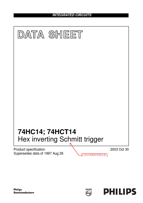
2003 Oct 30
2
Philips Semiconductors
The 74HC14 and 74HCT14 provide six inverting buffers with Schmitt-trigger action. They are capable of transforming slowly changing input signals into sharply defined, jitter-free output signals.
GND 7
14 VCC 13 6A
12 6Y
14
11 5A
10 5Y
9 4A
8 4Y
MNA839
Fig.1 Pin configuration.
handbook, halfpage
1Y 2
1A VCC 1 14
13 6A
2A 3 2Y 4
GND(1)
12 6Y 11 5A
3A 5
10 5Y
3Y 6
7
17
CI
input capacitance
3.5
3.5
CPD
power dissipation capacitance per gate notes 1 and 2
7
8
Notes
1. CPD is used to determine the dynamic power dissipation (PD in µW): PD = CPD × VCC2 × fi × N + Σ(CL × VCC2 × fo) where: fi = input frequency in MHz; fo = output frequency in MHz; CL = output load capacitance in pF; VCC = supply voltage in Volts; N = total load switching outputs; Σ(CL × VCC2 × fo) = sum of the outputs.
CHI MEI PA-765B E56070 元件说明书

•Component •元件UL file numberUL档案号Part number型号Remark备注Vendor供应商•FRONT CASE•前身E56070 PA-765B CHI MEI•TOP CASE•上身E56070 PA-765B CHI MEI•BOTTOM CASE•下身E56070 PA-765B CHI MEI•Batterycompartment•电池箱E207780 PC945(GG) QMFZ2 SABIC JAPAN L L C•Transformercover•火牛上盖E50075 LV2250V TEIJIN•TransformerHousing 火牛下盖E50075 LV2250V TEIJIN•Aux foam pad•Aux盖E257267 E50A-60 ZHI JIN•Side plate•侧盖E56070 PA-765B CHI MEI•Battery BayRubber Cover•电池箱盖E257267 E50A-60 ZHI JIN•batterydoors•电池盖E56070 PA-765B CHI MEI•AAA batterycover•3A 电池门E56070 PA-765B CHI MEI•Light guide•导光片E54705 CL PMMA SUMIPEX•Frontcontrolpanel 显示压件E248280 PC+ABS Jacobson•Strainrelief•线卡E107293 6P-4 晋煜•Power cord •电源线E137516 SJTW ZJCZ 利源電業製品廠有限公司LEE YUEN ELECTRICAL MFY LTD. E143681 LY-13B ELBZ7•Lead wire •引线E244721 UL 1007 20AWGL=330mmAVLV2 惠州市远达电业五金制品有限公司HUI ZHOU YUEN DA ELECTRONIC & HARDWARECO.,LTDE329541 UL 1007 18AWGVH3.96-H-2PVH3.96-TL=186mmZPFW2 深圳艾格科技有限公司Shenzhen Aiger Technology Co.,LtdE330646 UL 1007#24 XH-TXH-4P L=140mmAVLV2 深圳市展旺连接器有限公司Shen Zhen Zhan Wang Linker CO.,LTDE330646 UL 1007#24 XH-TXH-2P L=260mmAVLV2E330646 UL 2547#28 PH-TPH-3P L=260mmAVLV2E330646 UL 2547#28 PH-TPH-3P L=220mmAVLV2E330646 UL 1185 22AWG XH-T XH-2P L=150mmAVLV2•Integralfuse •保险丝E340427 SFC0800A(800mA/250V FastActing Glass TubeFuse)JDYX 瑞卓电子(东莞)有限公司Dongguan Reomax Electronics Co., LTD•Fuse Holder •保险丝座E239034 H3(10A/250V)IZLT2 惠州市海牛電子有限公司HUIZHOU HINEW ELECTRIC APPLIANCE CO.,LTD.变压器材料清單/ MATERIAL LISTNO. MATERIAL DESCRIPTION Ul file MANUFACTURERS / SUPPLIERS1. 膠芯/Bobbin 最小0.71mm厚尼龍66 101(r9)一層minimum 0.71mm thick PA66101(r9) one layerUL:E41938 杜邦/E I Dupont De Nemours & Co Inc2 膠套/Shroud 最小0.50mm厚尼龍66 101(r9)一層minimum 0.50mm thick PA66101(r9) one layerUL:E41938 杜邦/E I Dupont De Nemours & Co Inc3 初級線圈PrimaryWinding 聚氨酯漆包線MW75C(130℃) 或Polyurethane Wire,MW75C(130℃)UL:E258125 河源天裕電子塑膠有限公司He Yuan Sky Wealth Electronic And PlasticCo Ltd.4 初級跨線絕緣Pri. windingcrossoverinsulation CT25聚脂膠紙/CT-25 Polyestertape厚度:0.05mm*2 層/Thickness:0.05mm*2 layersUL:E165111 靖江亞華壓敏黏膠有限公司Jingjiang Yahua Pressure Sensitive Glue COLTD5 溫度保險Thermal Fuse Type: A4-F130 Deg.C ( 250V/2A)UL:E140847 雅寶電子有限公司/Aupo Electronics Inc.6 初級引線Primary Leads UL-1672 AWG #22 VW-1 300V105Deg.CUL:E191230UL:E189674UL:E211048UL:E214859恒輝(香港)發展有限公司Ever Bright (Hongkong) development CompanyLimited.深圳东聚Shenzhen Dong Ju Wire & CableCo.,Ltd.琦富瑞Qifurui Electronics co阳泰氟电线电缆YANGTAI WIRE & CABLE CO LTD7 初級引線Primary Leads 聚氨酯漆包線MW75C(130℃) 或Polyurethane Wire,MW75C(130℃)or聚氨酯漆包線MW79C(155℃)Polyurethane Wire,MW79C(155℃)UL:E258125UL:E201757河源天裕電子塑膠有限公司He Yuan Sky Wealth Electronic And PlasticCo Ltd.太平洋電線電纜深圳公司Pacific ElectricWire&Cable(shenzhen)Co.,Ltd.8 次級引線SecondaryLeads UL-1015 AWG #20 VW-1 600V105Deg.CUL:E191230UL:E189674UL:E211048UL:E214859恒輝(香港)發展有限公司Ever Bright(Hongkong) development Company Limited.深圳东聚Shenzhen Dong Ju Wire & CableCo.,Ltd.琦富瑞Qifurui Electronics co阳泰氟电线电缆YANGTAI WIRE & CABLE CO LTD9 次級引線SecondaryLeads CT25聚脂膠紙/CT-25 Polyestertape厚度:0.05mm*3 層/UL:E165111 靖江亞華壓敏黏膠有限公司Jingjiang Yahua Pressure Sensitive Glue COLTD.Thickness:0.05mm*3 layers聚酯膠片型號:MYLAR EL21 0.25mm厚PET film Type:MYLAR EL21 0.25mmThickUL:E93687 杜邦帝人/ Dupont Teijin Films U S L P10 外層絕緣Outinsulation CT25聚脂膠紙/CT-25 Polyestertape厚度:0.05mm*3 層/Thickness:0.05mm*3 layers聚酯膠片型號:MYLAR EL21 0.25mm厚PET film Type:MYLAR EL21 0.25mmThickUL:E165111UL:E93687靖江亞華壓敏黏膠有限公司Jingjiang Yahua Pressure Sensitive Glue COLTD.杜邦帝人/ Dupont Teijin Films U S L P11 鐵芯片LaminationCore EI-57 硅鋼片(H18 黑) 片厚0.50,疊厚35.3+/-0.5mmEI-57 silicon steel sheet(H18black), thickness:0.50mm,depth thickness:35.3+/-0.5mmN/A 東莞東駿電器有限公司Dongguan Dongjun Electrical Appliances Co.,Ltd.12 安裝架/Bracket 冷軋板鍍鋅Cold rolled Steel with Zinc-coatedN/A 東莞駿豐五金製品廠Dongguan JunFeng MetalManufactory13 屏蔽殼/Endbell 冷軋板鍍鋅Cold rolled Steel with Zinc-coatedN/A 東莞駿豐五金製品廠Dongguan JunFeng MetalManufactory14 次級連接器Secondaryconnector Housing: JS-1121-02 & Terminal:JS-1121-THousing: A3963H-2P & Terminal:A3963-TPUL: E113875UL: E326732喬訊電子有限公司Chyao shiunn electronicIndustrial Ltd.長江連接器有限公司ChangJiang Connectors CoLtd15 浸漬/Impregnation Insulating Varnish/絕緣油Type: 8562/C, class FUL:E200154 恒昌化學塗料公司HANG CHEUNG PETROCHEMICALLTD。
TPS2554 and TPS2555 Evaluation Module User's Guide
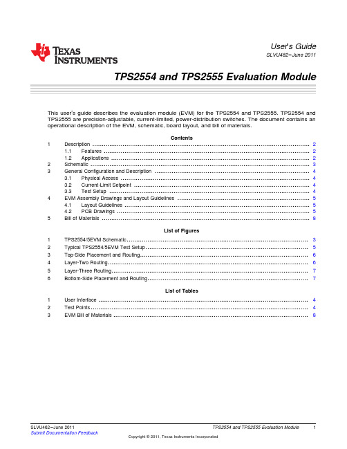
User's GuideSLVU462–June2011TPS2554and TPS2555Evaluation Module This user’s guide describes the evaluation module(EVM)for the TPS2554and TPS2555.TPS2554and TPS2555are precision-adjustable,current-limited,power-distribution switches.The document contains an operational description of the EVM,schematic,board layout,and bill of materials.Contents1Description (2)1.1Features (2)1.2Applications (2)2Schematic (3)3General Configuration and Description (4)3.1Physical Access (4)3.2Current-Limit Setpoint (4)3.3Test Setup (4)4EVM Assembly Drawings and Layout Guidelines (5)4.1Layout Guidelines (5)4.2PCB Drawings (5)5Bill of Materials (8)List of Figures1TPS2554/5EVM Schematic (3)2Typical TPS2554/5EVM Test Setup (5)3Top-Side Placement and Routing (6)4Layer-Two Routing (6)5Layer-Three Routing (7)6Bottom-Side Placement and Routing (7)List of Tables1User Interface (4)2Test Points (4)3EVM Bill of Materials (8)1 SLVU462–June2011TPS2554and TPS2555Evaluation Module Submit Documentation FeedbackCopyright©2011,Texas Instruments IncorporatedDescription 1DescriptionThe TPS2554EVM-010evaluation module allows reference circuit evaluation of the Texas Instruments TPS2554and TPS2555power-distribution switches.1.1Features•Precision adjustable,current-limited,power-distribution switch•Fast overcurrent response–1µs typical•80-mΩ,high-side MOSFET•Operating range:4.5V to5.5V1.2Applications•USB ports/hubs•Notebook personal computers(PC)2TPS2554and TPS2555Evaluation Module SLVU462–June2011Submit Documentation FeedbackCopyright©2011,Texas Instruments IncorporatedGeneral Configuration and Description 3General Configuration and Description3.1Physical AccessTable1lists the TPS2554/5EVM connector functionality,and Table2describes the test point availability.er InterfaceConnector Label DescriptionJ1VIN Input connectorJ2VOUT Output connectorJ3J3Input voltage jumper.Shunt can be removed to measure input current.J4J4Output voltage jumper.Shunt can be removed to measure output current.J5EN Enable jumper.Leave open to enable TPS2554and install shunt to enable TPS2555.J6ILIM_SEL Current limit select.Install shunt to select ILIM0(2.4A nominal),and remove shunt toselect ILIM1(1.2A nominal).D1(RED)FLT Fault LEDTable2.Test PointsTest Point Color Label DescriptionTP3RED IN Power switch input(IC side of J3shunt)TP4BLK GND Power switch input groundTP1WHT FLT Fault pin outputTP2RED VOUT Power switch outputTP5BLK GND Power switch output groundTP6WHT EN Enable pin input3.2Current-Limit SetpointR4and R5configure the current-limit setpoint for ILIM0and ILIM1,respectively(see J6in Table1).ILIM0or ILIM1setpoint can be adjusted using the following example by substituting R4or R5for RILIMx .In thisexample IOS=2A.The following example is an approximation only and does not take into account the resistor tolerance or the variation of ILIM.For exact variation of ILIM,see the TPS2554/TPS2555data sheet,SLVSAM0.IOS=48000/RILIMx=2ARILIMx=48000/IOS=48000/2=24000ΩChoose RILIMx=23.7kΩIOS=48000/23700=2.03A3.3Test SetupFigure2shows a typical test setup for TPS2554/5EVM.4TPS2554and TPS2555Evaluation Module SLVU462–June2011Submit Documentation FeedbackCopyright©2011,Texas Instruments IncorporatedV INOscilloscope EVM Assembly Drawings and Layout GuidelinesFigure2.Typical TPS2554/5EVM Test Setup4EVM Assembly Drawings and Layout Guidelines4.1Layout Guidelines•TPS2554/55placement:Place the TPS2554/55near the USB output connector and the150-µF OUT pin filter capacitor.Connect the exposed pad to the GND pin and the system ground plane using a viaarray.•IN pin bypass capacitance:Place the100-nF bypass capacitor near the IN and GND pins,and make the connection using a low-inductance trace.•ILIM0and ILIM1pin connections:Current-limit accuracy can be compromised by stray current leakage from a higher voltage source to the ILIM0or ILIM1pins.Ensure that adequate spacing existsbetween IN pin copper/trace and ILIM0pin trace to prevent contaminate buildup during the PCBassembly process.If a low-current-limit setpoint is required(RILIMx >200kΩ),use ILIM1for this case,as it is further away from the IN pin.4.2PCB DrawingsThe Figure3through Figure6show component placement and layout of the EVM.5 SLVU462–June2011TPS2554and TPS2555Evaluation Module Submit Documentation FeedbackCopyright©2011,Texas Instruments IncorporatedEVM Assembly Drawings and Layout Guidelines Figure 3.Top-Side Placement and RoutingFigure yer-Two Routing6TPS2554and TPS2555Evaluation ModuleSLVU462–June 2011Submit Documentation FeedbackCopyright ©2011,Texas Instruments Incorporated EVM Assembly Drawings and Layout Guidelinesyer-Three RoutingFigure6.Bottom-Side Placement and Routing7 SLVU462–June2011TPS2554and TPS2555Evaluation Module Submit Documentation FeedbackCopyright©2011,Texas Instruments IncorporatedEvaluation Board/Kit Important NoticeTexas Instruments(TI)provides the enclosed product(s)under the following conditions:This evaluation board/kit is intended for use for ENGINEERING DEVELOPMENT,DEMONSTRATION,OR EVALUATION PURPOSES ONLY and is not considered by TI to be a finished end-product fit for general consumer use.Persons handling the product(s)must have electronics training and observe good engineering practice standards.As such,the goods being provided are not intended to be complete in terms of required design-,marketing-,and/or manufacturing-related protective considerations, including product safety and environmental measures typically found in end products that incorporate such semiconductor components or circuit boards.This evaluation board/kit does not fall within the scope of the European Union directives regarding electromagnetic compatibility,restricted substances(RoHS),recycling(WEEE),FCC,CE or UL,and therefore may not meet the technical requirements of these directives or other related directives.Should this evaluation board/kit not meet the specifications indicated in the User’s Guide,the board/kit may be returned within30 days from the date of delivery for a full refund.THE FOREGOING WARRANTY IS THE EXCLUSIVE WARRANTY MADE BY SELLER TO BUYER AND IS IN LIEU OF ALL OTHER WARRANTIES,EXPRESSED,IMPLIED,OR STATUTORY,INCLUDING ANY WARRANTY OF MERCHANTABILITY OR FITNESS FOR ANY PARTICULAR PURPOSE.The user assumes all responsibility and liability for proper and safe handling of the goods.Further,the user indemnifies TI from all claims arising from the handling or use of the goods.Due to the open construction of the product,it is the user’s responsibility to take any and all appropriate precautions with regard to electrostatic discharge.EXCEPT TO THE EXTENT OF THE INDEMNITY SET FORTH ABOVE,NEITHER PARTY SHALL BE LIABLE TO THE OTHER FOR ANY INDIRECT,SPECIAL,INCIDENTAL,OR CONSEQUENTIAL DAMAGES.TI currently deals with a variety of customers for products,and therefore our arrangement with the user is not exclusive.TI assumes no liability for applications assistance,customer product design,software performance,or infringement of patents or services described herein.Please read the User’s Guide and,specifically,the Warnings and Restrictions notice in the User’s Guide prior to handling the product.This notice contains important safety information about temperatures and voltages.For additional information on TI’s environmental and/or safety programs,please contact the TI application engineer or visit /esh.No license is granted under any patent right or other intellectual property right of TI covering or relating to any machine,process,or combination in which such TI products or services might be or are used.FCC WarningThis evaluation board/kit is intended for use for ENGINEERING DEVELOPMENT,DEMONSTRATION,OR EVALUATION PURPOSES ONLY and is not considered by TI to be a finished end-product fit for general consumer use.It generates,uses,and can radiate radio frequency energy and has not been tested for compliance with the limits of computing devices pursuant to part15 of FCC rules,which are designed to provide reasonable protection against radio frequency interference.Operation of this equipment in other environments may cause interference with radio communications,in which case the user at his own expense will be required to take whatever measures may be required to correct this interference.EVM Warnings and RestrictionsIt is important to operate this EVM within the input voltage range of0V to5.5V and the output voltage range of0V to5.5V. Exceeding the specified input range may cause unexpected operation and/or irreversible damage to the EVM.If there are questions concerning the input range,please contact a TI field representative prior to connecting the input power.Applying loads outside of the specified output range may result in unintended operation and/or possible permanent damage to the EVM.Please consult the EVM User's Guide prior to connecting any load to the EVM output.If there is uncertainty as to the load specification,please contact a TI field representative.During normal operation,some circuit components may have case temperatures greater than85°C.The EVM is designed to operate properly with certain components above85°C as long as the input and output ranges are maintained.These components include but are not limited to linear regulators,switching transistors,pass transistors,and current sense resistors.These types of devices can be identified using the EVM schematic located in the EVM User's Guide.When placing measurement probes near these devices during operation,please be aware that these devices may be very warm to the touch.Mailing Address:Texas Instruments,Post Office Box655303,Dallas,Texas75265Copyright©2011,Texas Instruments IncorporatedIMPORTANT NOTICETexas Instruments Incorporated and its subsidiaries(TI)reserve the right to make corrections,modifications,enhancements,improvements, and other changes to its products and services at any time and to discontinue any product or service without notice.Customers should obtain the latest relevant information before placing orders and should verify that such information is current and complete.All products are sold subject to TI’s terms and conditions of sale supplied at the time of order acknowledgment.TI warrants performance of its hardware products to the specifications applicable at the time of sale in accordance with TI’s standard warranty.Testing and other quality control techniques are used to the extent TI deems necessary to support this warranty.Except where mandated by government requirements,testing of all parameters of each product is not necessarily performed.TI assumes no liability for applications assistance or customer product design.Customers are responsible for their products and applications using TI components.To minimize the risks associated with customer products and applications,customers should provide adequate design and operating safeguards.TI does not warrant or represent that any license,either express or implied,is granted under any TI patent right,copyright,mask work right, or other TI intellectual property right relating to any combination,machine,or process in which TI products or services are rmation published by TI regarding third-party products or services does not constitute a license from TI to use such products or services or a warranty or endorsement e of such information may require a license from a third party under the patents or other intellectual property of the third party,or a license from TI under the patents or other intellectual property of TI.Reproduction of TI information in TI data books or data sheets is permissible only if reproduction is without alteration and is accompanied by all associated warranties,conditions,limitations,and notices.Reproduction of this information with alteration is an unfair and deceptive business practice.TI is not responsible or liable for such altered rmation of third parties may be subject to additional restrictions.Resale of TI products or services with statements different from or beyond the parameters stated by TI for that product or service voids all express and any implied warranties for the associated TI product or service and is an unfair and deceptive business practice.TI is not responsible or liable for any such statements.TI products are not authorized for use in safety-critical applications(such as life support)where a failure of the TI product would reasonably be expected to cause severe personal injury or death,unless officers of the parties have executed an agreement specifically governing such use.Buyers represent that they have all necessary expertise in the safety and regulatory ramifications of their applications,and acknowledge and agree that they are solely responsible for all legal,regulatory and safety-related requirements concerning their products and any use of TI products in such safety-critical applications,notwithstanding any applications-related information or support that may be provided by TI.Further,Buyers must fully indemnify TI and its representatives against any damages arising out of the use of TI products in such safety-critical applications.TI products are neither designed nor intended for use in military/aerospace applications or environments unless the TI products are specifically designated by TI as military-grade or"enhanced plastic."Only products designated by TI as military-grade meet military specifications.Buyers acknowledge and agree that any such use of TI products which TI has not designated as military-grade is solely at the Buyer's risk,and that they are solely responsible for compliance with all legal and regulatory requirements in connection with such use. TI products are neither designed nor intended for use in automotive applications or environments unless the specific TI products are designated by TI as compliant with ISO/TS16949requirements.Buyers acknowledge and agree that,if they use any non-designated products in automotive applications,TI will not be responsible for any failure to meet such requirements.Following are URLs where you can obtain information on other Texas Instruments products and application solutions:Products ApplicationsAudio /audio Communications and Telecom /communicationsAmplifiers Computers and Peripherals /computersData Converters Consumer Electronics /consumer-appsDLP®Products Energy and Lighting /energyDSP Industrial /industrialClocks and Timers /clocks Medical /medicalInterface Security /securityLogic Space,Avionics and Defense /space-avionics-defense Power Mgmt Transportation and /automotiveAutomotiveMicrocontrollers Video and Imaging /videoRFID Wireless /wireless-appsRF/IF and ZigBee®Solutions /lprfTI E2E Community Home Page Mailing Address:Texas Instruments,Post Office Box655303,Dallas,Texas75265Copyright©2011,Texas Instruments Incorporated。
HC2用户手册说明书

USER’S MANUALPORTABLE HIGH CURRENT TEST SETMODEL NUMBER HC2Version 4.1Phenix Technologies Inc.75 Speicher DriveAccident, Maryland 21520Copyright © Phenix Technologies, Inc.Rev 11/14/2016 nabTABLE OF CONTENTSDESCRIPTION SECTION NUMBERDANGER / GENERAL SAFETY PRECAUTIONSTECHNICAL SPECIFICATIONS 1 DEVICE WARNINGS 2 CONTROLS AND INDICATORS 3BASIC APPROACH TO TESTING 4 CALIBRATION 5PARTS LIST 6PARTS ORDERING INFORMATION 7 RECOMMENDED SPARE PARTS 8 RETURNED MATERIAL 9 ELECTRICAL SCHEMATICS 10 CUSTOMER COMMENTS / SUGGESTIONS 11WARNING !!Complete Grounding of this unit is necessary for the safe operation of this equipment. Disconnect inputs before un-grounding this equipmentGENERAL SAFETY PRECAUTIONSHIGH CURRENT/HIGH VOLTAGEThis equipment is capable of providing POTENTIALLY LETHAL VOLTAGESAND/OR SEVERE BURNS! Improper operation or test practices may result in injury or death to the operator or surrounding personnel.The operation of this test equipment should only be performed by personnel familiar with Electrical Testing and Safety Procedures. The operator of this equipment must be aware of all hazards associated with Electrical Testing. The operator is responsible for himself and others in close proximity of the testing area.Some General Safety Practices for working with Electrical Test Equipment have been listed below for your reference.∙Become familiar with your instrument before performing an actual test∙Know your work area, check that all circuits are de-energized and locked out.∙Never work alone; always work with another qualified worker.∙Mark off entire work area with barriers and warning tape as necessary.∙Make all personnel aware of your testing activities.∙Be aware of dangerous conditions that may arise from energizing a test specimen.∙Never modify test equipment, modifications to equipment could introduce an unknown hazard or hinder a designed-in safety feature.∙DO NOT operate damaged equipment. Remove power, and do not use the equipment until safe operation can be verified by service-trained personnel. Phenix Technologies, Inc. assumes no liability for unsafe or improper use of test equipment.SECTION 1: TECHNICAL SPECIFICATIONSThe HC2 is a portable high current test set built for field and shop use. Designed using the latest technology, the HC2 combines a variable high current output with appropriate controls and instrumentation for testing thermal, magnetic, and solid-state motor overload relays, molded-case circuit breakers, and ground fault trip devices. The HC2 can be used in many other applications requiring a high current source.The HC2 provides a short duration output of 2000 amps through a typical 200 amp molded-case circuit breaker when an instantaneous trip element must be tested. Sufficient current is available for testing time delay characteristics of motor overload relays and molded-case circuit breakers.The unique auto-sensing feature makes the HC2 easy to operate. Sensing leads, which operate on either normally-open or normally-closed (non-energized) devices, are connected to the test object auxiliary or non-energized contacts. The output current level can be easily pre-set. When the output is initiated, the pre-set output current locks on and the timer starts. When the test set senses a change in state of the test object auxiliary contacts (NO to NC or NC to NO), the current shuts off and the timer stops. If set to sense current, unit will shut current off at approximately 10% of range switch setting of currentmeter when test object goes open. For instantaneous trip tests, the memory feature of the currentmeter holds the peak current value until reset by the operator.TECHNICAL DATA AND SPECIFICATIONSINPUT: 120 Volts or 220 Volts (as ordered), 50 Hz or 60 Hz (must be preset)OUTPUT: 0-70 Volts at 25 amperes0-14 Volts at 125 amperes0-7 Volts at 250 amperes0-3.5 Volts at 500 amperesOVERLOAD:Short duration overloads are possible on each tap. The test set is capable ofup to 2000 amps, depending on the impedance of the test circuit.DUTY CYCLE:Continuous at 100%5 minutes ON/15 minutes OFF at 200%1 minute ON/5 minutes OFF at 300%30 seconds ON/5 minutes OFF at 400%INSTRUMENTATION:Currentmeter: 3 1/2 digit LCDRanges: 0-1.999/19.99/199.9/1999 amperesAccuracy: +/- .5%Timer: 6 digit LCD, in cycles or secondsRanges: 0-999999 cycles or 0-9999.99 secondsAccuracy: +/- 0.1% readingDIMENSIONS:21.25" W x 16.75" D x 13.75" H; 93 lbs. (220 V unit; 95 lbs.)(540mm W x 426 mm D x 350 mm H; 42.2 kg) (220 V unit; 43 kg)Cables: 11.5 lbs. (5.2 kg.)OUTPUT LEADS: 5 ft. sense control leads5 ft. high current leads (4/0 and 4 Ga)5 ft. low current leads (10 Ga)SECTION 2: DEVICE WARNINGS1. For safe operation, it is important that the unit be plugged into a properly grounded receptacle.2. This unit is not designed for use in energized circuits.3. Due to leakage current within the solid-state circuitry, it is STRONGLY RECOMMENDED to turn controlpower off when changing the output leads.4. NEVER connect sense jacks to energized contacts or terminals being injected by test unit.SECTION 3: CONTROLS AND INDICATORSHC2 Control Panel-1. MAIN POWER This circuit breaker controls the input power to the control and the power sections.2. OUTPUT This circuit breaker protects the variable transformer.3. F1 This protects the control circuitry and power supplies.4. HC ONWhen pressed, this allows current to flow from the unit (provided that the output is shorted as through a closed breaker). If this output current exceeds 10% of the selected output current range, the output will be maintained when the switch is released. Also, the TIMER will begin to run at this point.5. HC OFF When this is pressed, the output current will cease to flow from the unit.6. JOGThis switch is used when it is desired to preset output current to a specific level. When pressed, the output current will begin to flow as it would when HC ON ispressed. The difference is that the TIMER will not begin running in this mode, and the output current will cease to flow when the switch is released, regardless of its magnitude.12316151213111098754614CONTROLS AND INDICATORSHC2 Control Panel (Cont’d)7.RAISE CURRENT Controls current level from minimum to maximum of output tap when HC ON or JOGis activated. Use with JOG to preset current level through test object.8. RANGE SWITCH Four ranges available are 2 Amp (R84), 20 Amp (R85), 200 Amp (R-69), 2000 Amp(R73)9. CURRENTMETER This displays the RMS value of the output current level of the unit. There are fourranges available:2 Amp 1.99920 Amp 19.99200 Amp 199.92000 Amp 1999WARNING: Please note that there is no correlation between the currentmeterrange switch setting and the rating of the taps.MEM/CONT When set to the CONT (continuous) mode, the meter will continuously update todisplay the output current level. When placed in the MEM (memory) mode, the meterwill retain the highest output current level achieved. If the level again exceeds thisvalue, the meter will be updated. If you are below the highest level, pressing RESETwill update the meter to the present level of output.Please note that the MEM mode of operation will only maintain the reading for a shorttime before the reading starts to decay.10. TRIP/RESET This switch serves several purposes.1) When in CONTACTS mode, the lamp will illuminate to indicate that the non-energized contacts of the test specimen connected to the SENSE INPUTS haschanged states.2) When in CURRENT mode, the lamp will illuminate to indicate that the outputcurrent has dropped below the 10% level.3) When pressed, the TIMER will be reset to zero.4) When the CURRENTMETER MEM/CONT is set to the MEM mode, pressing resetwill release currentmeter from its highest registered reading. If the output currentis not at zero, the present output reading will be maintained until either the outputlevel increases, or the reset is pressed again.5) When illuminated, it must be pressed to reset controls for further operation.11. TIMER The timer will begin counting when HC ON is pressed and the current surpasses the10% level. The timer will stop when the current drops below the 10% level in theSENSE CURRENT mode. When in the SENSE CONTACTS mode, the timer will stopwhen a change in the SENSE INPUTS is detected.The timer can be set to read CYCLES or SECONDS.CONTROLS AND INDICATORS12. SENSE SWITCH This can be set to CONTACTS or CURRENT mode. When placed in CONTACTSmode, the unit will react to a change in condition of the SENSE INPUTS. Upon achange in condition, the TIMER will stop running and the output current will cease toflow. The TRIP lamp will illuminate as an indication to the operator of a change incondition.In CONTACTS mode, sense leads must be properly connected to non-energizedcontacts operated by the test specimen or the timer will not shut off when thetest specimen goes open. If the sense leads are not used, the sense switchmust be in CURRENT position for proper functioning.When the SENSE switch is set to the CURRENT mode, the unit will react to the outputcurrent dropping below 10% of the level of the selected current range.13. SENSE INPUTS These are connected to an auxiliary set of contacts (non-energized) regardless if theyare normally open or closed. When RESET is pressed, the unit will remember itsstate. If the state changes, the unit will react to this change if the SENSE switch is setto CONTACTS.CAUTION: Please do not attempt to connect these to the same set of contactswhich you intend to energize, or energized auxiliary contacts. This may causedamage to the unit.14. CONNECTORS Locations for 3 test connections (7 VAC, 250 A), (70 VAC 25 A), (14 VAC, 125 A).15. COMMON Electrical connection for test cable.16. CONNECTOR Test connection (3.5 VAC, 500 A).SECTION 4: BASIC APPROACH TO TESTINGThe HC2 is basically a continuously variable high current source, the magnitudes of which are dependent on the output tap that is selected. Please refer to the Technical Data andSpecifications for the voltage and current ratings of the taps.The output current is controlled by use of the RAISE CURRENT knob on the control panel. By turning the knob in the clockwise direction, the current is raised. By turning the knob in the counter-clockwise direction the output magnitude is decreased.The RMS value of the output current is displayed on the CURRENTMETER. If the MEM/CONT switch is in the CONT (for CONTinuous), the meter displays the real-time value of the output. If the MEM/CONT switch is in the MEM (for MEMory), the highest value of the output current is displayed.When a breaker is to be tested, the operator may select the SENSE CONTACTS mode or the SENSE CURRENT mode of operation. If an auxiliary set of non-energized contacts are available, the SENSE CONTACTS mode may be selected. By pressing JOG or RESET the state of the contacts (be it normally open or normally closed) are remembered by the unit. The operator may then preset the output current to the desired level by use of the JOG switch. When this is done, by pressing HC ON (and assuming that the current level exceeds 10% of the CURRENTMETER range selected), the current will continue flowing after the switch is released and the TIMER will begin to run.When the contacts connected to the SENSE INPUTS change state, the TIMER will stop running and the output current will cease to flow. The TRIP lamp will illuminate as an indication to the operator. If the MEM/CONT switch is in the MEM mode, the highest output current achieved will be displayed on the CURRENTMETER. The operator should note this level before the readings begin to decay. Pressing RESET will zero the TIMER and CURRENTMETER readings, and prepare the unit for operation again.When the SENSE switch is set to the CURRENT mode, the SENSE INPUTS are not used. This position was meant mainly for single pole breakers in which the SENSE INPUTS cannot be used. In this mode initiation of the test is the same as in SENSE CONTACTS mode. The difference is the completion of the test. When the output current falls below 10% of range (as when the contacts of the breaker open) the TIMER stops running and the output current turns off. The TRIP lamp illuminates as an indication to the operator.SECTION 5: CALIBRATIONTIMER The timer is run from a precision programmable oscillator and should never requirecalibration.CURRENTMETER The calibration of the currentmeter should be checked on a yearly basis. To do this, place the MEM/CONT switch in the CONT position. Place the range switch in the 2AMP range. With nothing connected to the output and the RAISE CURRENT knob inits fully counter-clockwise position, adjust R10 until the CURRENTMETER reads zero.With appropriate test equipment (RMS) raise the output current to 80% of each rangeand adjust the corresponding calibration potentiometer to agree with your standard.SECTION 6: HC-2 PARTS LISTSECTION 7: PARTS ORDERING INFORMATIONReplacement parts are available from Phenix Technologies, Inc.Changes to Phenix Technologies' products are sometimes made to accommodate improved components as they become available, and to give you the benefit of the latest technical improvements developed in our Engineering Department. It is, therefore, important when ordering parts to include the serial number of the unit as well as the part number of the replacement part.When your purchase order is received at our office, a representative of Phenix Technologies will contact you to confirm the current price of the part being ordered. If a part you order has been replaced with a new or improved part, an Applications Engineer will contact you concerning any change in part number.Send orders for replacement parts to:Service DepartmentPhenix Technologies, Inc.75 Speicher DriveAccident, Maryland 21520Ph 1 (301) 746-8118Fax: 1 (301) 895-5570E-mail:*******************SECTION 8: RECOMMENDED SPARE PARTSPhenix Technologies recommends that the customer purchase and stock the following parts for normal maintenance of the unit. The recommended quantity should be sufficient to support the unit during normal operation.If the unit will be operated at an isolated site for an extended period or will be subjected to unusual stresses, a larger quantity of parts should be stocked as spares. In such cases, contact Phenix Technologies for a recommendation.Current prices may be obtained by contacting the Service Department at Phenix Technologies.Part Name ComputerNumber Recommended QuantityLamps, 6.3 V, EAO 1420143 8 EAO Momentary – 1 POLE Switch (SW1, 3, 4, 5) 1860120 1 Binding Post – RED 1351102 1 Binding Post - BLACK 1351100 1 F1 (120V) 3 AG 3 Amp 1603603 1 F1 (220V) 3 AG 1.5 Amp 1603602 1 Current Meter – KNS 3 ½ digit 1506400 1 Timer – Red Lion Sub- Cub – D 1505420 1 Lens – Red EAO 1422150 1 Lens – Green EAO 1422151 1 Lens – Amber EAO 1422152 1SECTION 9: RETURNED MATERIALIf for any reason it should become necessary to return this equipment to the factory, the Service Department of Phenix Technologies, Inc. must be given the following information:Name Plate InformationModel NumberSerial NumberReason for ReturnCause of DefectIf Phenix Technologies, Inc. deems return of the part appropriate, it will then issue an "Authorization for Return." If return is not deemed advisable, other inspection arrangements will be made.NOTE: Material received at this plant without the proper authorization shall be held as"Customer's Property" with no service until such time as the proper steps have been taken.Your cooperation is requested in order to ensure prompt service.SECTION 10: ELECTRICAL SCHEMATICS Drawing Number Description1. 9304510 HC-2 Electrical Schematic (120V)2. 9304511 HC-2 Electrical Schematic (220V)SECTION 11: CUSTOMER COMMENTS/SUGGESTIONSPhenix Technologies made significant efforts to ensure that the materials in this Operator’s Manual are correct. If there are concerns or comments as you have used this information, Phenix Technologies appreciates any feedback.Unit Serial Number:Please return to Phenix Technologies, Engineering Department, 75 Speicher Drive, Accident, MD 21520 USA.Phone:1(301)746-8118,Fax1(301)895-5570,*********************。
- 1、下载文档前请自行甄别文档内容的完整性,平台不提供额外的编辑、内容补充、找答案等附加服务。
- 2、"仅部分预览"的文档,不可在线预览部分如存在完整性等问题,可反馈申请退款(可完整预览的文档不适用该条件!)。
- 3、如文档侵犯您的权益,请联系客服反馈,我们会尽快为您处理(人工客服工作时间:9:00-18:30)。
Product Name:
SB-742457CAS No.:
607742-69-8Cat. No.:
HY-14339Product Data Sheet
MWt:
353.44Formula:
C19H19N3O2S Purity :>98%
Solubility:
DMSO 78 mg/mL; Water <1 mg/mL
Mechanisms:Biological Activity:
SB742457is a highly selective 5-HT6receptor antagonist with pKi of 963;exhibits >100-fold
Pathways:GPCR/G protein; Target:5-HT Receptor
Pathways:Neuronal Signaling; Target:5-HT Receptor SB742457 is a highly selective 5HT6 receptor antagonist with pKi of 9.63; exhibits >100fold
selectivity over other receptors.
IC50 Value: 9.63 (pKi)
Target: 5-HT6 Receptor SB-742457, a 5-HT6 receptor antagonist, which extends into Alzheimer disease (AD) sufferers further highlights the therapeutic promise of this mechanistic approach. Alzheimer's disease is a devastating neurological condition characterized by a progressive decline in cognitive performance accompanied by behavioral and psychological syndromes, such as depression and psychosis. With the subsequent development of selective 5-HT6 receptor antagonists, preclinical studies in rodents References:
[1]. Callaghan CK, Hok V, Della-Chiesa A, et al. Age-related declines in delayed non-match-to-sample performance (DNMS) are reversed by the novel 5HT6 receptor antagonist SB742457.
Neuropharmacology. 2012 Oct;63(5):890-7.and primates have elucidated the function of this receptor subtype in more detail. It is increasingly clear that blockade of 5-HT6 receptors leads to an improvement of cognitive performance in a wide variety of learning and ...
p gy ;()[2]. Codony X, Vela JM, Ramírez MJ. 5-HT(6) receptor and cognition. Curr Opin Pharmacol. 2011
Feb;11(1):94-100.[3]. Maher-Edwards G, Dixon R, Hunter J, et al. SB-742457 and donepezil in Alzheimer disease: a
randomized, placebo-controlled study. Int J Geriatr Psychiatry. 2011 May;26(5):536-44.[4]. Maher-Edwards G, Zvartau-Hind M, Hunter AJ, et al. Double-blind, controlled phase II study of a 5-HT6 receptor antagonist, SB-742457, in Alzheimer's disease. Curr Alzheimer Res. 2010
Aug;7(5):374-85.[5]. Upton N, Chuang TT, Hunter AJ, Virley DJ. 5-HT6 receptor antagonists as novel cognitive h i f Al h i 'di N h Caution: Not fully tested. For research purposes only
Medchemexpress LLC
enhancing agents for Alzheimer's disease. Neurother...
18 W i l k i n s o n W a y , P r i n c e t o n , N J 08540,U S A
E m a i l : i n f o @m e d c h e m e x p r e s s .c o m W e b : w w w .m e d c h e m e x p r e s s .c o m。