MAX5933E中文资料
MAX3490EESA+中文资料
General DescriptionDevices in the MAX3483E family (MAX3483E/MAX3485E/MAX3486E/MAX3488E/MAX3490E/MAX3491E) are ±15kV ESD-protected, +3.3V, low-power transceivers for RS-485 and RS-422 communications. Each device con-tains one driver and one receiver. The MAX3483E and MAX3488E feature slew-rate-limited drivers that minimize EMI and reduce reflections caused by improperly termi-nated cables, allowing error-free data transmission at data rates up to 250kbps. The partially slew-rate-limited MAX3486E transmits up to 2.5Mbps. The MAX3485E,MAX3490E, and MAX3491E transmit at up to 12Mbps.All devices feature enhanced electrostatic discharge (ESD) protection. All transmitter outputs and receiver inputs are protected to ±15kV using IEC 1000-4-2 Air-Gap Discharge, ±8kV using IEC 1000-4-2 Contact Discharge, and ±15kV using the Human Body Model.Drivers are short-circuit current limited and are protect-ed against excessive power dissipation by thermal shutdown circuitry that places the driver outputs into a high-impedance state. The receiver input has a fail-safe feature that guarantees a logic-high output if both inputs are open circuit.The MAX3488E, MAX3490E, and MAX3491E feature full-duplex communication, while the MAX3483E,MAX3485E, and MAX3486E are designed for half-duplex communication.ApplicationsTelecommunicationsIndustrial-Control Local Area Networks Transceivers for EMI-Sensitive Applications Integrated Services Digital Networks Packet SwitchingFeatureso ESD Protection for RS-485 I/O Pins±15kV—Human Body Model±8kV—IEC 1000-4-2, Contact Discharge ±15kV—IEC 1000-4-2, Air-Gap Discharge o Operate from a Single +3.3V Supply—No Charge Pump Required o Interoperable with +5V Logic o Guaranteed 12Mbps Data Rate (MAX3485E/MAX3490E/MAX3491E)o Slew-Rate Limited for Errorless Data Transmission (MAX3483E/MAX3488E) o 2nA Low-Current Shutdown Mode(MAX3483E/MAX3485E/MAX3486E/MAX3491E)o -7V to +12V Common-Mode Input Voltage Range o Full-Duplex and Half-Duplex Versions Available o Industry-Standard 75176 Pinout (MAX3483E/MAX3485E/MAX3486E)o Current-Limiting and Thermal Shutdown for Driver Overload ProtectionMAX3483E/MAX3485E/MAX3486E/MAX3488E/MAX3490E/MAX3491E3.3V-Powered, ±15kV ESD-Protected, 12Mbps and Slew-Rate-Limited T rue RS-485/RS-422 T ransceivers________________________________________________________________Maxim Integrated Products119-1474; Rev 0; 4/99Selector GuideOrdering InformationOrdering Information continued at end of data sheet.For free samples & the latest literature: , or phone 1-800-998-8800.For small orders, phone 1-800-835-8769.M A X 3483E /M A X 3485E /M A X 3486E /M A X 3488E /M A X 3490E /M A X 3491E3.3V-Powered, ±15kV ESD-Protected, 12Mbps and Slew-Rate-Limited T rue RS-485/RS-422 T ransceiversABSOLUTE MAXIMUM RATINGSDC ELECTRICAL CHARACTERISTICS(V = +3.3V ±0.3V, T = T to T , unless otherwise noted. Typical values are at T = +25°C.)Stresses beyond those listed under “Absolute Maximum Ratings” may cause permanent damage to the device. These are stress ratings only, and functional operation of the device at these or any other conditions beyond those indicated in the operational sections of the specifications is not implied. Exposure to absolute maximum rating conditions for extended periods may affect device reliability.Supply Voltage (V CC ).............................................................+7V Control Input Voltage (RE , DE).................................-0.3V to +7V Driver Input Voltage (DI)...........................................-0.3V to +7V Driver Output Voltage (A, B, Y, Z).......................-7.5V to +12.5V Receiver Input Voltage (A, B)..............................-7.5V to +12.5V Receiver Output Voltage (RO)....................-0.3V to (V CC + 0.3V)Continuous Power Dissipation (T A = +70°C)8-Pin SO (derate 5.88mW/°C above +70°C)..................471mW 8-Pin Plastic DIP (derate 9.09mW/°C above +70°C).....727mW14-Pin SO (derate 8.33mW/°C above +70°C)................667mW 14-Pin Plastic DIP (derate 10mW/°C above +70°C)......800mW Operating Temperature RangesMAX34_ _ EC_ _...................................................0°C to +70°C MAX34_ _ EE_ _.................................................-40°C to +85°C Storage Temperature Range.............................-65°C to +150°C Lead Temperature (soldering, 10sec).............................+300°CMAX3483E/MAX3485E/MAX3486E/MAX3488E/MAX3490E/MAX3491E3.3V-Powered, ±15kV ESD-Protected, 12Mbps and Slew-Rate-Limited T rue RS-485/RS-422 T ransceiversDC ELECTRICAL CHARACTERISTICS (continued)(V CC = +3.3V ±0.3V, T A = T MIN to T MAX , unless otherwise noted. Typical values are at T A = +25°C.)DRIVER SWITCHING CHARACTERISTICS—MAX3485E/MAX3490E/MAX3491E(V = +3.3V, T = +25°C.)DRIVER SWITCHING CHARACTERISTICS—MAX3486E(V = +3.3V, T = +25°C.)*MAX3488E and MAX3491E will be compliant to ±8kV per IEC 1000-4-2 Contact Discharge by September 1999.M A X 3483E /M A X 3485E /M A X 3486E /M A X 3488E /M A X 3490E /M A X 3491E3.3V-Powered, ±15kV ESD-Protected, 12Mbps and Slew-Rate-Limited T rue RS-485/RS-422 T ransceivers4_______________________________________________________________________________________DRIVER SWITCHING CHARACTERISTICS—MAX3483E/MAX3488E(V CC = +3.3V, T A = +25°C.)RECEIVER SWITCHING CHARACTERISTICS(V CC = +3.3V, T A = +25°C.)Note 1:∆V OD and ∆V OC are the changes in V OD and V OC , respectively, when the DI input changes state.Note 2:Measured on |t PLH (Y) - t PHL (Y)|and |t PLH (Z) - t PHL (Z)|.Note 3:The transceivers are put into shutdown by bringing RE high and DE low. If the inputs are in this state for less than 80ns, thedevices are guaranteed not to enter shutdown. If the inputs are in this state for at least 300ns, the devices are guaranteed to have entered shutdown. See Low-Power Shutdown Mode section.MAX3483E/MAX3485E/MAX3486E/MAX3488E/MAX3490E/MAX3491E3.3V-Powered, ±15kV ESD-Protected, 12Mbps and Slew-Rate-Limited T rue RS-485/RS-422 T ransceivers_______________________________________________________________________________________5Typical Operating Characteristics(V CC = +3.3V, T A = +25°C, unless otherwise noted.)252015105000.51.01.52.02.53.53.0OUTPUT CURRENT vs.RECEIVER OUTPUT LOW VOLTAGEM A X 3483E -01OUTPUT LOW VOLTAGE (V)O U T P U T C U R R E N T (m A )-20-18-16-14-12-10-8-6-4-2000.51.01.52.02.53.53.0OUTPUT CURRENT vs.RECEIVER OUTPUT HIGH VOLTAGEM A X 3483E -02OUTPUT HIGH VOLTAGE (V)O U T P U T C U R R E N T (m A )3.003.053.103.153.203.253.30-40-20020406010080RECEIVER OUTPUT HIGH VOLTAGEvs. TEMPERATURETEMPERATURE (°C)O U T P U T H I G H V O L T A G E (V )00.10.20.30.40.50.60.70.8-40-2020406010080RECEIVER OUTPUT LOW VOLTAGEvs. TEMPERATURETEMPERATURE (°C)O U T P U T L O W V O L T A G E (V )2505075100125150175024681012OUTPUT CURRENT vs.DRIVER OUTPUT LOW VOLTAGEM A X 3483E -07OUTPUT LOW VOLTAGE (V)O U T P U T C U R R E N T (m A )100908070605040302010000.5 1.0 1.5 2.0 2.5 3.53.0DRIVER OUTPUT CURRENT vs.DIFFERENTIAL OUTPUT VOLTAGEM A X 3483E -05DIFFERENTIAL OUTPUT VOLTAGE (V)O U T P U T C U R R E N T (m A )1.61.71.81.92.02.12.22.32.42.62.5-40-20020406010080DRIVER DIFFERENTIAL OUTPUT VOLTAGE vs. TEMPERATURETEMPERATURE (°C)D I F FE R E N T I A L O U T P U T V O L T A G E (V )-100-80-60-40-20543210-7-6-3-4-5-2-1OUTPUT CURRENT vs.DRIVER OUTPUT HIGH VOLTAGEM A X 3483E -08OUTPUT HIGH VOLTAGE (V)O U T P U T C U R R E N T (m A )M A X 3483E /M A X 3485E /M A X 3486E /M A X 3488E /M A X 3490E /M A X 3491E3.3V-Powered, ±15kV ESD-Protected, 12Mbps and Slew-Rate-Limited T rue RS-485/RS-422 T ransceivers0.80.70.91.01.11.2-40-2020406010080SUPPLY CURRENT vs. TEMPERATURETEMPERATURE (°C)S U P P L Y C U R R E N T (m A )Typical Operating Characteristics (continued)(V CC = +3.3V, T A = +25°C, unless otherwise noted.)0102030405060708010090-40-2020406010080SHUTDOWN CURRENT vs. TEMPERATUREM A X 3483E -10TEMPERATURE (°C)S H U T D O W N C U R R E N T (n A )Pin DescriptionMAX3483E/MAX3485E/MAX3486E/MAX3488E/MAX3490E/MAX3491E3.3V-Powered, ±15kV ESD-Protected, 12Mbps and Slew-Rate-Limited T rue RS-485/RS-422 T ransceivers_______________________________________________________________________________________7Figure 2. MAX3488E/MAX3490E Pin Configuration and Typical Operating CircuitFigure 3. MAX3491E Pin Configuration and Typical Operating CircuitFigure 1. MAX3483E/MAX3485E/MAX3486E Pin Configuration and Typical Operating CircuitM A X 3483E /M A X 3485E /M A X 3486E /M A X 3488E /M A X 3490E /M A X 3491E3.3V-Powered, ±15kV ESD-Protected, 12Mbps and Slew-Rate-Limited T rue RS-485/RS-422 T ransceivers8_______________________________________________________________________________________Figure 4. Driver V OD and V OC Figure 7. Driver Differential Output Delay and Transition TimesFigure 6. Receiver V OH and V OLFigure 5. Driver V OD with Varying Common-Mode VoltageMAX3483E/MAX3485E/MAX3486E/MAX3488E/MAX3490E/MAX3491E3.3V-Powered, ±15kV ESD-Protected, 12Mbps and Slew-Rate-Limited T rue RS-485/RS-422 T ransceivers_______________________________________________________________________________________9Figure 8. Driver Propagation TimesFigure 9. Driver Enable and Disable Times (t PZH , t PSH , t PHZ )Figure 10. Driver Enable and Disable Times (t PZL , t PSL , t PLZ )M A X 3483E /M A X 3485E /M A X 3486E /M A X 3488E /M A X 3490E /M A X 3491E3.3V-Powered, ±15kV ESD-Protected, 12Mbps and Slew-Rate-Limited T rue RS-485/RS-422 T ransceivers10______________________________________________________________________________________Figure 11. Receiver Propagation DelayFigure 12. Receiver Enable and Disable TimesNote 4: The input pulse is supplied by a generator with the following characteristics: f = 250kHz, 50% duty cycle, t r ≤6.0ns, Z O = 50Ω.Note 5: C L includes probe and stray capacitance._____________________Function TablesDevices with Receiver/Driver Enable(MAX3483E/MAX3485E/MAX3486E/MAX3491E)Table 1. Transmitting* B and A outputs are Z and Y, respectively, for full-duplex part (MAX3491E).X = Don’t care; High-Z = High impedanceTable 2. Receiving* DE is a “don’t care” (x) for the full-duplex part (MAX3491E).X = Don’t care; High-Z = High impedanceDevices without Receiver/Driver Enable(MAX3488E/MAX3490E)Table 3. TransmittingTable 4. Receiving___________Applications InformationThe MAX3483E/MAX3485E/MAX3486E/MAX3488E/MAX3490E/MAX3491E are low-power transceivers for RS-485 and RS-422 communications. The MAX3483E and MAX3488E can transmit and receive at data rates up to 250kbps, the MAX3486E at up to 2.5Mbps, and the MAX3485E/MAX3490E/MAX3491E at up to 12Mbps. The MAX3488E/MAX3490E/MAX3491E are full-duplex trans-ceivers, while the MAX3483E/MAX3485E/MAX3486E are half-duplex. Driver Enable (DE) and Receiver Enable (RE ) pins are included on the MAX3483E/MAX3485E/MAX3486E/MAX3491E. When disabled, the driver and receiver outputs are high impedance.Reduced EMI and Reflections (MAX3483E/MAX3486E/MAX3488E)The MAX3483E/MAX3488E are slew-rate limited, mini-mizing EMI and reducing reflections caused by improp-erly terminated cables. Figure 13 shows the driver output waveform of a MAX3485E/MAX3490E/MAX3491E transmitting a 125kHz signal, as well as the Fourier analysis of that waveform. High-frequency harmonics with large amplitudes are evident. Figure 14 shows the same information, but for the slew-rate-limited MAX3483E/MAX3488E transmitting the same signal. The high-frequency harmonics have much lower amplitudes,and the potential for EMI is significantly reduced.Low-Power Shutdown Mode(MAX3483E/MAX3485E/MAX3486E/MAX3491E)A low-power shutdown mode is initiated by bringing both RE high and DE low. The devices will not shut down unless both the driver and receiver are disabled (high impedance). In shutdown, the devices typically draw only 2nA of supply current.For these devices, the t PSH and t PSL enable times assume the part was in the low-power shutdown mode;the t PZH and t PZL enable times assume the receiver or driver was disabled, but the part was not shut down.MAX3483E/MAX3485E/MAX3486E/MAX3488E/MAX3490E/MAX3491E3.3V-Powered, ±15kV ESD-Protected, 12Mbps and Slew-Rate-Limited T rue RS-485/RS-422 T ransceivers______________________________________________________________________________________11INPUTS OUTPUT A, B RO ≥+0.2V 1≤-0.2V 0Inputs Open1INPUT OUTPUTS DI Z Y 101015MHz 500kHz/div 05MHz500kHz/div Figure 13. Driver Output Waveform and FFT Plot of MAX3485E/MAX3490E/MAX3491E Transmitting a 125kHz Signal Figure 14. Driver Output Waveform and FFT Plot of MAX3483E/ MAX3488E Transmitting a 125kHz SignalM A X 3483E /M A X 3485E /M A X 3486E /M A X 3488E /M A X 3490E /M A X 3491E3.3V-Powered, ±15kV ESD-Protected, 12Mbps and Slew-Rate-Limited T rue RS-485/RS-422 T ransceivers12______________________________________________________________________________________Figure 17. MAX3483E/MAX3488E Driver Propagation Delay Figure 19. MAX3483E/MAX3488E System Differential Voltage at 125kHz Driving 4000 Feet of Cable Figure 20. MAX3485E/MAX3490E/MAX3491E System Differential Voltage at 125kHz Driving 4000 Feet of CableDriver-Output Protection Excessive output current and power dissipation caused by faults or by bus contention are prevented by two mechanisms. A foldback current limit on the output stage provides immediate protection against short circuits over the whole common-mode voltage range (see Typical Operating Characteristics). In addition, a thermal shut-down circuit forces the driver outputs into a high-imped-ance state if the die temperature rises excessively.Propagation Delay Figures 15–18 show the typical propagation delays. Skew time is simply the difference between the low-to-high and high-to-low propagation delay. Small driver/receiver skew times help maintain a symmetrical mark-space ratio (50% duty cycle).The receiver skew time, |t PRLH- t PRHL|, is under 10ns (20ns for the MAX3483E/MAX3488E). The driver skew times are 8ns for the MAX3485E/MAX3490E/MAX3491E, 12ns for the MAX3486E, and typically under 50ns for the MAX3483E/MAX3488E.Line Length vs. Data Rate The RS-485/RS-422 standard covers line lengths up to 4000 feet. For line lengths greater than 4000 feet, see Figure 21 for an example of a line repeater.Figures 19 and 20 show the system differential voltage for parts driving 4000 feet of 26AWG twisted-pair wire at 125kHz into 120Ωloads.For faster data rate transmission, please consult the fac-tory.±15kV ESD Protection As with all Maxim devices, ESD-protection structures are incorporated on all pins to protect against electrostatic discharges encountered during handling and assembly. The driver outputs and receiver inputs of the MAX3483E family of devices have extra protection against static electricity. Maxim’s engineers have developed state-of-the-art structures to protect these pins against ESD of ±15kV without damage. The ESD structures withstand high ESD in all states: normal operation, shutdown, and powered down. After an ESD event, Maxim’s E versions keep working without latchup or damage.ESD protection can be tested in various ways; the transmitter outputs and receiver inputs of this product family are characterized for protection to the following limits:1)±15kV using the Human Body Model2)±8kV using the Contact-Discharge method specifiedin IEC 1000-4-23)±15kV using IEC 1000-4-2’s Air-Gap method.ESD Test Conditions ESD performance depends on a variety of conditions. Contact Maxim for a reliability report that documents test setup, test methodology, and test results.Human Body Model Figure 22a shows the Human Body Model and Figure 22b shows the current waveform it generates when dis-charged into a low impedance. This model consists of a 100pF capacitor charged to the ESD voltage of inter-est, which is then discharged into the test device through a 1.5kΩresistor.IEC 1000-4-2 The IEC 1000-4-2 standard covers ESD testing and performance of finished equipment; it does not specifi-cally refer to integrated circuits. The MAX3483E family of devices helps you design equipment that meets Level 4 (the highest level) of IEC 1000-4-2, without the need for additional ESD-protection components.The major difference between tests done using the Human Body Model and IEC 1000-4-2 is higher peak current in IEC 1000-4-2, because series resistance is lower in the IEC 1000-4-2 model. Hence, the ESD with-stand voltage measured to IEC 1000-4-2 is generally lower than that measured using the Human Body Model. Figure 23a shows the IEC 1000-4-2 model, and Figure 23b shows the current waveform for the ±8kV IEC 1000-4-2, Level 4 ESD contact-discharge test.Figure 21. Line Repeater for MAX3488E/MAX3490E/MAX3491EMAX3483E/MAX3485E/MAX3486E/MAX3488E/MAX3490E/MAX3491E3.3V-Powered, ±15kV ESD-Protected, 12Mbps and Slew-Rate-Limited T rue RS-485/RS-422 T ransceivers ______________________________________________________________________________________13M A X 3483E /M A X 3485E /M A X 3486E /M A X 3488E /M A X 3490E /M A X 3491EThe air-gap test involves approaching the device with a charged probe. The contact-discharge method connects the probe to the device before the probe is energized.Machine ModelThe Machine Model for ESD tests all pins using a 200pF storage capacitor and zero discharge resis-tance. Its objective is to emulate the stress caused when I/O pins are contacted by handling equipment during test and assembly. Of course, all pins require this protection, not just RS-485 inputs and outputs.Typical ApplicationsThe MAX3483E/MAX3485E/MAX3486E/MAX3488E/MAX3490E/MAX3491E transceivers are designed for bidirectional data communications on multipoint bus transmission lines. Figures 24 and 25 show typical net-work applications circuits. These parts can also be used as line repeaters, with cable lengths longer than 4000 feet, as shown in Figure 21.To minimize reflections, the line should be terminated at both ends in its characteristic impedance, and stub lengths off the main line should be kept as short as possible. The slew-rate-limited MAX3483E/MAX3488E and the partially slew-rate-limited MAX3486E are more tolerant of imperfect termination.3.3V-Powered, ±15kV ESD-Protected, 12Mbps and Slew-Rate-Limited T rue RS-485/RS-422 T ransceivers14______________________________________________________________________________________Figure 22a. Human Body ESD Test ModelFigure 22b. Human Body Current WaveformFigure 23a. IEC 1000-4-2 ESD Test ModelFigure 23b. IEC 1000-4-2 ESD Generator Current WaveformMAX3483E/MAX3485E/MAX3486E/MAX3488E/MAX3490E/MAX3491E3.3V-Powered, ±15kV ESD-Protected, 12Mbps and Slew-Rate-Limited T rue RS-485/RS-422 T ransceivers______________________________________________________________________________________15Figure 25. MAX3488E/MAX3490E/MAX3491E Full-Duplex RS-485 NetworkFigure 24. MAX3483E/MAX3485E/MAX3486E Typical RS-485 NetworkM A X 3483E /M A X 3485E /M A X 3486E /M A X 3488E /M A X 3490E /M A X 3491E3.3V-Powered, ±15kV ESD-Protected, 12Mbps and Slew-Rate-Limited T rue RS-485/RS-422 T ransceiversTRANSISTOR COUNT: 761Chip InformationOrdering Information (continued)Maxim cannot assume responsibility for use of any circuitry other than circuitry entirely embodied in a Maxim product. No circuit patent licenses are implied. Maxim reserves the right to change the circuitry and specifications without notice at any time.16____________________Maxim Integrated Products, 120 San Gabriel Drive, Sunnyvale, CA 94086 408-737-7600©1999 Maxim Integrated ProductsPrinted USAis a registered trademark of Maxim Integrated Products.。
3933中文资料

Data Sheet 26301.100†The A3933SEQ is a three-phase MOSFET controller for use with bipolar brushless dc motors. It drives all n-channel external power FETs, allowing system cost savings and minimizing r (DS)on power loss.The high-side drive block is implemented with bootstrap capacitors at each output to provide the floating positive supply for the gate drive.The high-side circuitry also employs a unique “intelligent” FETmonitoring circuit that ensures the gate voltages are at the proper levels before turn-on and during the ON cycle. This device is targeted for applications with motor supplies from 12 V to 28 V.Internal fixed off-time PWM current-control circuitry can be used to regulate the maximum load current to a desired value. The peak load-current limit is set by the user’s selection of an input reference voltage and external sensing resistor. The fixed off-time pulse duration is set by a user-selected external RC timing network.A power-loss braking circuit brakes the motor on an under-voltage condition. The device is configured to either coast or dynamically brake the motor when this occurs.The A3933SEQ is supplied in a 32-lead rectangular (9 x 7) plasticchip carrier (quad pack) for minimum-area, surface-mount applica-tions.3933FEATURES AND BENEFITSI Drives External N-Channel FETs I Intelligent High-Side Gate DriveI Selectable Coast or Dynamic Brake on Power Down I Adjustable Dead Time for Cross-Conduction Protection I Selectable Fast or Slow Current-Decay Modes I Internal PWM Peak Current Control I Reset/Coast InputI 120° Hall Commutation with Internal Pullup I Internal 5-V RegulatorI Low-Side Synchronous Rectification I Direction ControlI PWM Speed-Control Input I Fault-Diagnostic Output IUnder-Voltage ProtectionTHREE-PHASE POWER MOSFET CONTROLLER115 Northeast Cutoff, Box 15036Worcester, Massachusetts 01615-0036 (508) 853-********THREE-PHASE POWER MOSFET CONTROLLERCopyright © 1999, Allegro MicroSystems, Inc.Functional Block DiagramRECOMMENDED OPERATING CONDITIONSSupply Voltage, V BB ...................................... 15 V to 28 Vor, if V BB = V CCOUT ................................... 12 V ±10%Logic Input Voltage Range, V IN .............. -0.3 V to +4.8 V Sense Voltage Range, V SENSE ........................ -1 V to +1 V RC Resistance.......................................... 10 k Ω to 100 k ΩPWM Frequency, f PWM ....................... 20 kHz to 100 kHzLOW-SIDE Dwg. FP-045V 1 OF 3 HIGH-SIDE DRIVERSTO 1 OF 3MOTOR PHASES TO LCAP3933THREE-PHASE POWER MOSFET CONTROLLERELECTRICAL SPECIFICATIONS at T A = 25°C, V BB = V CCOUT = 12 V, C load = 1000 pF, C boot = 0.047 µF (unless noted otherwise).LimitsParameterSymbolConditionsMinTypMaxUnitsSupply CurrentQuiescent Current I BB RESET low, f PWM = 40 kHz –1619mA RESET high–1517mA Reference Voltage V LCAP4.755.0 5.25V Ref. Volt. Load Regulation ∆V LCAP(∆ILCAP)I LCAP = 0 to -2 mA –1025mV Output VoltageV CCOUTV BB = 28 V10.81213.2V Output Voltage Regulation∆V CCOUT(∆ICCOUT)V BB = 28 V, I CCOUT = 0 to -10 mA––25mV Digital Logic LevelsLogic Input Voltage V IH 2.0––V V IL ––0.8V Logic Input CurrentI IH V IH = 2 V –<1.010µA I ILV IL = 0.8 V-70–-130µA Gate DriveLow-Side Output Voltage V GLxH 9.510.511.5V V GLxL I GLx = 1 mA––0.30V High-Side Output Voltage V GHxH 9.010.511.5V V GHxL I GHx = 1 mA ––0.25V Low-Side Output t rGLx 1 V to 8 V –50–ns Switching Time t fGLx 8 V to 1 V –40–ns High-Side Output t rGHx 1 V to 8 V –100–ns Switching Time t fGHx 8 V to 1 V –100–ns DEAD Timet DEADI DEAD = 10 µA –3000–ns (Source OFF to Sink ON)I DEAD = 215 µA –180–nsContinued —NOTES: 1.Typical Data is for design information only.2.Negative current is defined as coming out of (sourcing) the specified device terminal.115 Northeast Cutoff, Box 15036Worcester, Massachusetts 01615-0036 (508) 853-50003933THREE-PHASE POWER MOSFET CONTROLLERELECTRICAL SPECIFICATIONS at T A = 25°C, V BB = V CCOUT = 12 V, C load = 0.001 µF, C boot = 0.047 µF (unless noted otherwise), continued.LimitsParameterSymbolConditions MinTypMaxUnitsBootstrap CapacitorBootstrap Charge Current I Cx 50100150mA Bootstrap Output Voltage V Cx Reference Sx9.510.511.5V Leakage CurrentI Cx High side switched high, Sx = V BB–1520µA Current LimitOffset Voltage V io –0±5.0mV Input bias current I SENSE ––-1.0µA RC Charge Current I RC 8509451040µA RC Voltage Threshold V RCL 1.0 1.1 1.2V V RCH 2.73.0 3.2V PWM frequency Rangef PWM Operating 20–100kHz Protection CircuitryUndervoltage Threshold UVLO Increasing V BB 9.710.210.7V Decreasing V BB 9.35–10.35V Boot-Strap Capacitor Volt.V CxSx V BB = 12 V 9.5––V High-Side Gate-Source Volt.V GHxSx – 6.3–V Fault Output VoltageV FAULT I O = 1 mA––0.8V Brake FunctionBrake Cap. Supply Current I BRKCAP V BB = 8 V, BRKSEL ≥ 2 V –30–µA Low-Side Gate VoltageV GLxHV BB = 0, BRKCAP = 8 V–6.6–VNOTES: 1.Typical Data is for design information only.2.Negative current is defined as coming out of (sourcing) the specified device terminal.3933THREE-PHASE POWER MOSFET CONTROLLERTerminalName1PGND 2RESET 3GLC 4SC 5GHC 6CC 7GLB 8SB 9GHB 10CB 11GLA 12SA 13GHA 14CA 15V CCOUT 16LCAP 17FAULT 18MODE 19V BB 20H121H322H223DIR 24BRAKE 25BRKCAP 26BRKSEL 27PWM 28RC 29SENSE 30REF 31DEAD 32AGNDRESET — A logic input used to enable the device, internally pulled up to V LCAP (+5 V). A logic HIGH will disable the device and force all gate drivers to 0 V, coasting the motor. A logic LOW allows the gate drive to follow commutation logic.This input overrides BRAKE.GLA/GLB/GLC — Low-side, gate-drive outputs for external NMOS drivers. External series-gate resistors (as close aspossible to the NMOS gate) can be used to control the slew rate seen at the power-driver gate, thereby controlling the di/dt and dv/dt of the SA/SB/SC outputs. Each output is designed and specified to drive a 1000 pF load with a rise time of 50 ns.SA/SB/SC — Directly connected to the motor, these terminals sense the voltages switched across the load. These terminals are also connected to the negative side of the bootstrap capaci-tors and are the negative supply connections for the floating high-side drive.GHA/GHB/GHC — High-side, gate-drive outputs for external NMOS drivers. External series-gate resistors (as close aspossible to the NMOS gate) can be used to control the slew rate seen at the power-driver gate, thereby controlling the di/dt and dv/dt of the SA/SB/SC outputs. Each output is designed and specified to drive a 1000 pF load with a rise time of 100 ns.CA/CB/CC — High-side connections for the bootstrap capaci-tors, positive supply for high-side gate drive. The bootstrap capacitor is charged to approximately V CCOUT when theassociated output SA/SB/SC terminal is low. When the output swings high, the voltage on this terminal rises with the output to provide the boosted gate voltage needed for n-channel power FETs.Terminal Descriptionscontinued next page115 Northeast Cutoff, Box 15036Worcester, Massachusetts 01615-0036 (508) 853-50003933THREE-PHASE POWER MOSFET CONTROLLERFAULT — Open-drain output to indicate fault condition; will go active high for any of the following:1 – invalid HALL input code,2 – high-side, gate-source voltage less than 7 V,3 – bootstrap capacitor not sufficiently charged, or4 – under-voltage condition detected at V CCOUT .The fault state for gate-source and bootstrap monitors are cleared at each commutation. If the motor has stalled, then the fault can only be cleared by toggling the RESET terminal or power-up sequence.MODE — A logic input to set current-decay method, internally pulled up to V LCAP (+5 V). When in slow-decay mode (logic HIGH), only the high-side FET is switched open during a PWM OFF cycle. The fast-decay mode (logic LOW) switches both the source and sink FETs.H1/H2/H3 — Hall-sensor inputs; internally pulled up to V LCAP (+5 V). Configured for 120° electrical spacing.DIR — A logic input to reverse rotation, see commutation logic table. Internally pulled up to V LCAP (+5 V).BRAKE — A logic input to short out the motor windings for a braking function. A logic HIGH will turn ON the low-side FETs, turn OFF the high-side FETs. Internally pulled up to V LCAP (+5 V). The braking torque applied will depend on the speed.BRKCAP — Connection for reservoir capacitor. This terminal is used to provide a positive power supply for the sink-drive outputs for a power-down condition. This will allow predict-able braking, if desired. A blocking diode to V CCOUT is re-quired. A 4.7 µF capacitor will provide 6.5 V gate drive for 300 ms. If a power-down braking option is not needed(BRKSEL = LOW) then this terminal should be tied to V CCOUT .BRKSEL — A logic input to enable/disable braking on power-down condition. Internally pulled up to V LCAP (+5 V). If held low, the motor will coast on a power-down condition.PWM — Speed control input, internally pulled up to V LCAP(+5 V). A logic LOW turns OFF all drivers, a logic HIGH will turn ON selected drivers as determined by H1/H2/H3 input logic. Holding the terminal high allows speed/torque control solely by the current-limit circuit via REF analog voltage command.RC — An analog input used to set the fixed off time with an external resistor (R T ) and capacitor (C T ). The t blank time is controlled by the value of the external capacitor (see Applica-tions Information). As a rule, the fixed off time should not be less than 10 µs. The resistor should be in the range of 10 k Ω to 100 k Ω.SENSE — An analog input to the current-limit comparator.A voltage representing load current appears on this terminal during ON time, when it reaches REF voltage, the comparator trips and load current decays for the fixed off-time interval.Voltage transients seen at this terminal when the drivers turn ON are ignored for time t blank .REF — An analog input to the current-limit comparator.Voltage applied here sets the peak load current.I peak = V REF /R S .V CCOUT — A regulated 12 V output; supply for low-side gate drive and bootstrap capacitor charge circuits. It is good practice to connect a decoupling capacitor from this terminal to AGND,as close to the device terminals as possible. The terminal should be shorted to V BB for 12 V applications.V BB — The A3933 supply voltage. It is good practice toconnect a decoupling capacitor from this terminal to AGND, as close to the device terminals as possible. This terminal should be shorted to V CCOUT for 12 V applications.LCAP — Connection for decoupling capacitor for the internal 5 V reference. This terminal can source no more than 2 mA.DEAD — An analog input. A resistor between DEAD and LCAP is selected to adjust turn-off to turn-on time. This delay is needed to prevent shoot-through in the external power FETs.The allowable resistor range is 20 k Ω to 430 k Ω, whichconverts to deadtime of 210 ns to 2.1 µs, using the following equation:t DEAD = (6.75 x 10⁻¹² x R DEAD ) + (75 x 10-9).AGND — The low-level (analog) reference point for the A3933.PGND — The reference point for all low-side gate drivers.Terminal Descriptions (cont’d)3933 THREE-PHASE POWER MOSFET CONTROLLER Commutation Truth TableLogic Inputs Driver OutputsH1H2H3DIR GLA GLB GLC GHA GHB GHC SA SB SCH L H H L L H H L L H Z L H L L H L L H L H L Z H L H H L H H L L L H L L H Z L H L H H L L L L H L Z H L H H H L H L L L H Z L H L L H H L H L H L L H L Z H L H L H L L L L H L Z H H L L L L H L L L H Z L H H H L L L H L H L L H L Z L H L L L L H H L L H Z L L H H L L L H L H L Z H L L L H L H L L L H L L H ZInput LogicMODE PWM RESET Mode OperationL L L Fast decay PWM chop mode, current decayL H L Fast decay Peak current limit, selected drivers ONH L L Slow decay PWM chop mode. current decayH H L Slow decay Peak current limit, selected drivers ONX X H Coast All gate drive outputs OFF, clear fault logicBrake ControlBRAKE BRKSEL Normal Operation Under Voltage or Power Loss ConditionL L Normal run mode Coast, all gate drive outputs OFFL H Normal run mode Dynamic brake, all sink gate drives ONH L Dynamic brake, all sink gate drives ON Coast, all gate drive outputs OFFH H Dynamic brake, all sink gate drives ON Dynamic brake, all sink gate drives ONL = Low Level, H = High Level, X = Don’t Care, Z = High Impedance115 Northeast Cutoff, Box 15036Worcester, Massachusetts 01615-0036 (508) 853-50003933THREE-PHASE POWER MOSFET CONTROLLERApplications Informationbootstrap capacitor. When the bootstrap capacitor has been properly charged, the high side is turned back ON. The circuit will allow three faults of this type within one commutation cycle before signaling a fault and coast the motor (all gate outputs go low).2)Bootstrap Monitor. The bootstrap capacitor is charged whenever a sink-side MOSFET is ON, Sx output goes low, and the load current recirculates. This happens constantly during normal operation. A 60 µs timer is started at the beginning of this cycle and the capacitor is charged with typically 100 mA.The bootstrap capacitor voltage is clamped at approximately 87% of V CCOUT . If the capacitor is not charged to the clamp voltage in 60 µs, a fault is signaled and the motor will coast.3)Undervoltage. The internal V CCOUT regulator supplies the low-side gate driver and the bootstrap charge current. It is critical to ensure that the voltages are at a proper level before enabling any of the outputs. The undervoltage circuit is active during power up and will force a motor coast condition until V CCOUT is greater than approximately 10 V.4)Hall Invalid. Illegal codes for the HALL inputs (000 or 111) will force a fault and coast the motor.Faults are cleared at the beginning of each commutation. If a stalled motor results from a fault, the fault can only be cleared by toggling the RESET terminal or by a power-up sequence.Current Control. Internal fixed off-time PWM circuitry is implemented to limit load current to a desired value. The external sense resistor combined with the applied analog voltage to REF terminal will set the peak current level approximatelyI TRIP ≈ V REF /R S .After the peak level is reached, the sense comparator trips and the load current will decay for a fixed off time.An external resistor (R T ) and capacitor (C T ) are used to set the fixed off-time period (t off = R T x C T ). The t off should be in the range of 10 µs to 50 µs. Longer values for t off can result in audible noise problems.Torque control can be implemented by varying the REF input voltage as long as the PWM input stays high. If direct control of the torque/current is desired by PWM input, a voltage can be applied to the REF input to set an absolute maximum current limit.Bootstrap Capacitor Selection. The high-side bootstrap circuit operates on a charge-transfer principle. The gate charge (Q g ) specification of the external power MOSFET must betaken into consideration. The bootstrap capacitor must be large enough to turn on the MOSFET without losing significant gate voltage. If the bootstrap capacitor is too large, it would take too long to charge up during the off portion of the PWM cycle. The capacitor value must be selected with both of these constraints in mind.1)Minimum bootstrap capacitor value to transfer charge. The charge on the bootstrap capacitor should be 20x greater than the gate charge (Q g ) of the power MOSFET.Example: For Q g = 0.025 µC, selectC boot = 20 x Q g /10.5 V = 0.047 µF.Check for maximum V g drop at turn on: dq = C boot x dV g , where Q g = dq.dV g = dq/C boot = 0.025 µC/0.047 µF = 532 mV.2)Calculate minimum PWM “OFF” cycle with C boot = 0.047 µF.dt = r o x C boot x ln(0.036/[Q g /C boot + 0.036])where r o = 20 ohms, the equivalent internal series resistance of the bootstrap capacitor monitor circuit.The sink-side MOSFET will be held OFF for this minimum time such that the bootstrap capacitor can be recharged independently of the PWM input frequency.The above equation is valid for PWM cycles after the bootstrap capacitor has been charged once. For the first cycle after a motor phase commutates from Hi-Z to GHx ON, or during the first charging cycle at power-up, the circuit will ignore PWM signals until it has been charged.The time required to charge up at power up and at commutation change is approximately:t = C boot x 7 V/0.1 AProtection Circuitry. The A3933 will protect the external MOSFETs by shutting down the gate drive if any of the following conditions are detected:1)Gate Source Monitor (high side only). The voltage on the GHx terminals must stay 7 V higher than the source. If this voltage droops below the threshold, the high side turns OFF,and the low-side gate will turn ON in an attempt to recharge the3933 THREE-PHASE POWER MOSFET CONTROLLER Applications Information (cont’d)PWM Blank. The capacitor (C T) also serves as the means to set the blank time duration. After the off time expires, the selected gates are turned back ON. At this time, large current transients can occur during the reverse recovery time (t rr) of the intrinsic body diodes of the external MOSFETs. To prevent the current-sense comparator from thinking the current spikes are a real overcurrent event, the comparator is blanked:t blank = 1.9 x C T/(1 mA-2/R T)The user must ensure that C T is large enough to cover the current-spike duration.Load Current Recirculation. If MODE has been set for slow decay, the high-side (source) driver will turn OFF forcing the current to recirculate through the pair of sink MOSFETs. If MODE has been selected for fast decay, both the selected high-and low-side gates are turned OFF, which will force the current to recirculate through one sink MOSFET and the high-side clamp diode. Synchronous rectification (only on the low side) allows current to flow through the MOSFET, rather than the clamp diode, during the decay time. This will minimize power loss during the off period. It is important to take into account that, when switching, the intrinsic diodes will conduct during the adjustable deadtime.Braking. The A3933 will dynamically brake by forcing all sink-side MOSFETs ON. This will effectively short out the BEMF. During braking, the load current can be approximated by:I BRAKE = V BEMF/R LPower Loss Brake. The BRKCAP and BRKSEL terminals provide a power-down braking option. By applying a logic level to input BRKSEL, the system can control if the motor is dynamically braked or is allowed to coast during an undervoltage event. The reservoir capacitor on the BRKCAP terminal provides the power to hold the sink-side gates ON after supply voltage is lost. A logic high on BRKSEL will brake the motor, a logic low and it will coast.Layout. Careful consideration must be given to PCB layout when designing high-frequency, fast-switching, high-current circuits.1)The analog ground (AGND), the power ground (PGND), and the high-current return of the external MOSFETs (the negative side of the sense resistor) should return separately to the negative side of the motor supply filtering capacitor. This will minimize the effect of switching noise on the device logic and analog reference.2)Minimize stray inductances by using short, wide copper runs at the drain and source terminals of all power MOSFETs. This includes motor lead connections, the input power buss, and the common source of the low-side power MOSFETs. This will minimize voltages induced by fast switching of large load currents.3)Kelvin connect the SENSE terminal PC trace to the positive side of the sense resistor.115 Northeast Cutoff, Box 15036Worcester, Massachusetts 01615-0036 (508) 853-50003933THREE-PHASE POWER MOSFET CONTROLLERDimensions in Inches(controlling dimensions)Dwg. MA-006-32 in5NOTES: 1. Lead spacing tolerance is non-cumulative.2. Exact body and lead configuration at vendor’s option within limits shown3933THREE-PHASE POWER MOSFET CONTROLLERDimensions in Millimeters(for reference only)Dwg. MA-006-32 mm5201413NOTES: 1. Lead spacing tolerance is non-cumulative.2. Exact body and lead configuration at vendor’s option within limits shownThe products described here are manufactured under one or more U.S.patents or U.S. patents pending.Allegro MicroSystems, Inc. reserves the right to make, from time totime, such departures from the detail specifications as may be required topermit improvements in the performance, reliability, or manufacturabilityof its products. Before placing an order, the user is cautioned to verify thatthe information being relied upon is current.Allegro products are not authorized for use as critical components inlife-support devices or systems without express written approval.The information included herein is believed to be accurate and reliable.However, Allegro MicroSystems, Inc. assumes no responsibility for its use;nor for any infringement of patents or other rights of third parties whichmay result from its use.115 Northeast Cutoff, Box 15036Worcester, Massachusetts 01615-0036 (508) 853-********THREE-PHASE POWER MOSFET CONTROLLERMOTOR DRIVERS FunctionOutput Ratings*Part Number †INTEGRATED CIRCUITS FOR BRUSHLESS DC MOTORS3-Phase Power MOSFET Controller —28 V 39333-Phase Power MOSFET Controller —50 V 39323-Phase Power MOSFET Controller —50 V 76002-Phase Hall-Effect Sensor/Driver 400 mA 26 V 3626Bidirectional 3-Phase Back-EMF Controller/Driver ±600 mA 14 V 89062-Phase Hall-Effect Sensor/Driver 900 mA 14 V 36253-Phase Back-EMF Controller/Driver ±900 mA 14 V 8902–A3-Phase Controller/Drivers ±2.0 A 45 V 2936 & 2936-120INTEGRATED BRIDGE DRIVERS FOR DC AND BIPOLAR STEPPER MOTORSDual Full Bridge with Protection & Diagnostics ±500 mA 30 V 3976PWM Current-Controlled Dual Full Bridge ±650 mA 30 V 3966PWM Current-Controlled Dual Full Bridge ±650 mA 30 V 3968PWM Current-Controlled Dual Full Bridge ±750 mA 45 V 2916PWM Current-Controlled Dual Full Bridge ±750 mA 45 V 2919PWM Current-Controlled Dual Full Bridge ±750 mA 45 V 6219PWM Current-Controlled Dual Full Bridge ±800 mA 33 V 3964PWM Current-Controlled Full Bridge ±1.3 A 50 V 3953PWM Current-Controlled Dual Full Bridge ±1.5 A 45 V 2917PWM Current-Controlled Dual Full Bridge ±1.5 A 45 V 2918PWM Current-Controlled Microstepping Full Bridge ±1.5 A 50 V 3955PWM Current-Controlled Microstepping Full Bridge ±1.5 A 50 V 3957PWM Current-Controlled Dual DMOS Full Bridge ±1.5 A 50 V 3972Dual Full-Bridge Driver ±2.0 A 50 V 2998PWM Current-Controlled Full Bridge ±2.0 A 50 V 3952DMOS Full Bridge PWM Driver ±2.0 A 50 V 3958Dual DMOS Full Bridge ±2.5 A 50 V 3971UNIPOLAR STEPPER MOTOR & OTHER DRIVERSVoice-Coil Motor Driver ±500 mA 6 V 8932–A Voice-Coil Motor Driver ±800 mA 16 V 8958Unipolar Stepper-Motor Quad Drivers 1 A 46 V 7024 & 7029Unipolar Microstepper-Motor Quad Driver 1.2 A 46 V 7042Unipolar Stepper-Motor Translator/Driver 1.25 A 50 V 5804Unipolar Stepper-Motor Quad Driver 1.8 A 50 V 2540Unipolar Stepper-Motor Quad Driver 1.8 A 50 V 2544Unipolar Stepper-Motor Quad Driver 3 A 46 V 7026Unipolar Microstepper-Motor Quad Driver 3 A 46 V 7044*Current is maximum specified test condition, voltage is maximum rating. See specification for sustaining voltage limits or over-current protection voltage limits. Negative current is defined as coming out of (sourcing) the output.†Complete part number includes additional characters to indicate operating temperature range and package style.Also, see 3175, 3177, 3235, and 3275 Hall-effect sensors for use with brushless dc motors.。
AD5933工作原理

AD5933工作原理AD5933是一款频率扫描阻抗测量系统,具有精确测量复杂阻抗的能力。
它是一款高性能的网络阻抗测量芯片,采用了混频器和锁相放大器的结构设计,在测量过程中,通过改变扫频信号的频率,可以快速获取待测物体的阻抗信息。
下面将详细介绍AD5933的工作原理。
首先,频率扫描部分。
AD5933通过产生一个连续的频率扫描信号来扫描待测物体的阻抗。
频率扫描信号是一个由数字控制的电流源产生的正弦波信号,其频率可以根据应用需求进行设置。
频率扫描信号经过一个可编程增益放大器进行放大,并进一步送入到待测物体中。
其次,信号处理部分。
AD5933采用了混频器和锁相放大器的技术来处理待测物体上的反射信号。
当频率扫描信号经过待测物体后,待测物体会发生阻抗变化导致信号的反射。
AD5933通过混频器将反射信号与参考信号进行混频,产生直流分量。
混频后的信号经过一个低通滤波器进行滤波,得到待测物体的实部和虚部。
最后,数据输出部分。
AD5933将经过信号处理后的实部和虚部输出到外部的微处理器或者计算机进行进一步处理。
这些数据可以用于计算待测物体的阻抗模数、相位、电阻、电感和电容等相关参数。
除了基本的工作原理外,AD5933还具有一些特殊的功能。
首先,它采用了对数放大器来提高动态范围和测量精度。
对数放大器可以将阻抗范围扩展到几个数量级,使得AD5933能够测量低阻抗和高阻抗的物体。
其次,AD5933还具有自动增益控制(AGC)功能,可以自动调整放大器的增益,以适应不同的测量环境。
此外,AD5933还支持外部参考电压输入和外部时钟输入,以满足特殊应用需求。
综上所述,AD5933是一款高性能的频率扫描阻抗测量系统。
它通过改变扫频信号的频率来获取待测物体的阻抗信息,并通过混频器和锁相放大器的结构设计实现了精确的测量。
AD5933具有广泛的应用领域,例如生物医学、材料科学、化学工程等。
它的工作原理简单明了,操作方便,能够提供准确可靠的测量结果。
MAX1239MEEE中文资料
Stresses beyond those listed under “Absolute Maximum Ratings” may cause permanent damage to the device. These are stress ratings only, and functional operation of the device at these or any other conditions beyond those indicated in the operational sections of the specifications is not implied. Exposure to absolute maximum rating conditions for extended periods may affect device reliability.
MAX1236–MAX1239
♦ ♦
Applications
Hand-Held Portable Applications Medical Instruments Battery-Powered Test Equipment Solar-Powered Remote Systems Received-Signal-Strength Indicators System Supervision
________________________________________________________________ Maxim Integrated Products
For pricing, delivery, and ordering information, please contact Maxim/Dallas Direct! at 1-888-629-4642, or visit Maxim’s website at .
AD5933应用
阻抗测量芯片AD5933原理及其应用时间:2010-03-04 23:48:25 来源:作者:1 AD5933芯片概述1.1 主要性能AD5933是一款高精度的阻抗测量芯片,内部集成了带有12位,采样率高达1MSPS的AD转换器的频率发生器。
这个频率发生器可以产生特定的频率来激励外部电阻,电阻上得到的响应信号被ADC采样,并通过片上的DSP进行离散的傅立叶变换。
傅立叶变换后返回在这个输出频率下得到的实部值R和虚部值I。
这样就可以很容易的计算出在每个扫描频率下的傅立叶变换的模和电阻的相角。
其中模=,相角=。
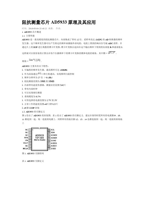
AD5933主要具有以下特性:λ可编程的频率发生器,最高频率可达100KHzλ作为设备通过口和主机通讯,实现频率扫面控制λ频率分辨率为27位(<0.1Hz)λ阻抗测量范围为100Ω到10MΩλ内部带有温度传感器,测量误差范围为±2℃λ带有内部时钟λ可以实现相位测量λ系统精度为0.5%λ可供选择的电源范围为2.7V到5Vλ正常工作的温度范围-40℃到+125℃λ 16脚SSOP封装1.2 AD5933的引脚定义图1给出了AD5933的封装图,表1给出了AD5933的引脚定义。
建议在使用时把所有的电源脚9、10、11都连到一起,统一连接到电源上,同样所有的地引脚12、13、14也都连接到一起,统一连接到系统地上图1 AD5933引脚排列表1 AD5933引脚定义1.3 主要应用AD5933可以广泛的应用在电化学分析、生物电极阻抗测量、阻抗谱分析、复杂阻抗测量、腐蚀监视和仪器保护、生物医学和自动控制传感器、无创检测、原材料性能分析以及燃料和电池状态监测等众多领域。
为阻抗的测量提供了很大的方便,单片集成技术大大的减小了仪器的体积,使得仪器使用更加方便。
简单的I2C通讯方式,方便用户操作,减小了用户编程的困难。
由于它给出的直接是变换后阻抗的实部和虚部数据,大大的简化了用户编程过程,节省了开发时间。
1SMA5918BT3G中文资料

1SMA5913BT3 Series1.5 Watt PlasticSurface MountZener Voltage RegulatorsThis complete new line of 1.5 Watt Zener Diodes offers the following advantages.Features•Standard Zener Breakdown V oltage Range − 3.3 V to 68 V •ESD Rating of Class 3 (>16 kV) per Human Body Model •Flat Handling Surface for Accurate Placement •Package Design for Top Slide or Bottom Circuit Board Mounting •Low Profile Package•Ideal Replacement for MELF Packages•Pb−Free Packages are AvailableMechanical Characteristics:CASE:V oid-free, transfer-molded plasticFINISH:All external surfaces are corrosion resistant with readily solderable leadsMAXIMUM CASE TEMPERATURE FOR SOLDERING PURPOSES: 260°C for 10 secondsPOLARITY:Cathode indicated by molded polarity notch or cathode bandFLAMMABILITY RATING:UL 94 V−0 @ 0.125 inMAXIMUM RATINGSRating Symbol Value UnitDC Power Dissipation @ T L = 75°C, Measured Zero Lead Length (Note 1) Derate above 75°CThermal Resistance, Junction−to−LeadP DR q JL1.52050WmW/°C°C/WDC Power Dissipation @ T A = 25°C (Note 2) Derate above 25°CThermal Resistance, Junction−to−AmbientP DR q JA0.54.0250WmW/°C°C/WOperating and Storage Temperature Range T J, T stg−65 to+150°CStresses exceeding Maximum Ratings may damage the device. Maximum Ratings are stress ratings only. Functional operation above the Recommended Operating Conditions is not implied. Extended exposure to stresses above the Recommended Operating Conditions may affect device reliability.1. 1 in square copper pad, FR−4 board.2.FR−4 Board, using ON Semiconductor minimum recommended footprint.Device Package Shipping†ORDERING INFORMATION1SMA59xxBT3SMA5000/Tape & Reel1SMA59xxBT3G SMA(Pb−Free)5000/Tape & Reel†For information on tape and reel specifications, including part orientation and tape sizes, please refer to our T ape and Reel Packaging Specifications Brochure, BRD8011/D.See specific marking information in the device marking column of the Electrical Characteristics table on page 2 of this data sheet.DEVICE MARKING INFORMATIONELECTRICAL CHARACTERISTICS (T A = 25°C unlessotherwise noted, V F = 1.5 V Max. @ I F = 200 mA for all types)Symbol ParameterV Z Reverse Zener Voltage @ I ZT I ZT Reverse CurrentZ ZT Maximum Zener Impedance @ I ZT I ZK Reverse CurrentZ ZK Maximum Zener Impedance @ I ZK I R Reverse Leakage Current @ V R V R Reverse Voltage I F Forward Current V F Forward Voltage @ I F I ZMMaximum DC Zener CurrentELECTRICAL CHARACTERISTICS (T A = 25°C unless otherwise noted, V F = 1.5 V Max. @ I F = 200 mA for all types)Device* (Note 3)Device Marking Zener Voltage (Note 4)Zener Impedance Leakage CurrentI ZM V Z (Volts)@ I ZT Z ZT @ I ZTZ ZK @ I ZK I R @ V R Min Nom Max mA W W mA m A Volts mA(dc)1SMA5913BT3, G 813B 3.13 3.3 3.47113.610500 1.050 1.04551SMA5914BT3, G 814B 3.42 3.6 3.78104.29.0500 1.035.5 1.04171SMA5915BT3, G 815B 3.70 3.9 4.1096.17.5500 1.012.5 1.03851SMA5916BT3, G 816B 4.08 4.3 4.5287.2 6.0500 1.0 2.5 1.03491SMA5917BT3, G 817B 4.46 4.7 4.9479.8 5.0500 1.0 2.5 1.53191SMA5918BT3, G 818B 4.84 5.1 5.3673.5 4.0350 1.0 2.5 2.02941SMA5919BT3, G 819B 5.32 5.6 5.8866.9 2.0250 1.0 2.5 3.02681SMA5920BT3, G 820B 5.89 6.2 6.5160.5 2.0200 1.0 2.5 4.02421SMA5921BT3, G 821B 6.46 6.87.1455.1 2.5200 1.0 2.5 5.22211SMA5922BT3, G 822B 7.127.57.8850 3.04000.5 2.5 6.02001SMA5923BT3, G 823B 7.798.28.6145.7 3.54000.5 2.5 6.51831SMA5924BT3, G 824B 8.649.19.5641.2 4.05000.5 2.57.01651SMA5925BT3, G 825B 9.51010.537.5 4.55000.25 2.58.01501SMA5926BT3, G 826B 10.451111.5534.1 5.55500.250.58.41361SMA5927BT3, G 827B 11.41212.631.2 6.55500.250.59.11251SMA5928BT3, G 828B 12.351313.6528.87.05500.250.59.91151SMA5929BT3, G 829B 14.251515.75259.06000.250.511.41001SMA5930BT3, G 830B 15.21616.823.4106000.250.512.2941SMA5931BT3, G 831B 17.11818.920.8126500.250.513.7831SMA5932BT3, G 832B 19202118.7146500.250.515.2751SMA5933BT3, G 833B 20.92223.11717.56500.250.516.7681SMA5934BT3, G 834B 22.82425.215.6197000.250.518.2631SMA5935BT3, G 835B 25.652728.3513.9237000.250.520.6561SMA5936BT3, G 836B 28.53031.512.5267500.250.522.8501SMA5937BT3, G 837B 31.353334.6511.4338000.250.525.1451SMA5938BT3, G 838B 34.23637.810.4388500.250.527.4421SMA5939BT3, G 839B 37.053940.959.6459000.250.529.7381SMA5940BT3, G840B40.854345.158.7539500.250.532.7351SMA5941BT3, G 841B 44.654749.358.06710000.250.535.8321SMA5942BT3, G 842B 48.455153.557.37011000.250.538.8291SMA5943BT3, G 843B 53.25658.8 6.78613000.250.542.6271SMA5944BT3, G 844B 58.96265.1 6.010015000.250.547.1241SMA5945BT3, G 845B 64.66871.4 5.512017000.250.551.7223.Tolerance and Voltage Regulation Designation − The type number listed indicates a tolerance of ±5%.4.V Z limits are to be guaranteed at thermal equilibrium.*The “G” suffix indicates Pb−Free package available.Figure 1. Steady State Power DeratingFigure 2. V Z − 3.3 thru 10 VoltsT, TEMPERATURE (°C)Figure 3. V Z = 12 thru 68 VoltsP D , M A X I M U MP O W E R D I S S I P A T I O N (W A T T S )I Z , Z E N E R C U R R E N T (m A )Z Z , D Y N A M I C I M P ED A N CE (O H M S )1002468101010.1V Z , ZENER VOLTAGE (VOLTS)1001010.1010203040V Z , ZENER VOLTAGE (VOLTS)V Z , ZENER VOLTAGE (VOLTS)1001050Figure 4. Zener Voltage − 3.3 to 12 VoltsFigure 5. Zener Voltage − 12 to 68 Volts Figure 6. Effect of Zener VoltageI Z , Z E N E R C U R R E N T (m A )6070801086420−2−4V Z , ZENER VOLTAGE (VOLTS), T E M P E R A T U R E C O E F F I C I E N T (m V / C )°θV Z 10070503020101020305070100V Z , ZENER VOLTAGE (VOLTS), T E M P E R A T U R E C O E F F I C I E N T (m V / C )°θV ZPACKAGE DIMENSIONSSMACASE 403D−02ISSUE Cǒmm inchesǓSCALE 8:1*For additional information on our Pb−Free strategy and solderingdetails, please download the ON Semiconductor Soldering and Mounting Techniques Reference Manual, SOLDERRM/D.SOLDERING FOOTPRINT*DIM A MIN NOM MAX MINMILLIMETERS1.912.16 2.410.075INCHES A10.050.100.150.002b 1.27 1.45 1.630.050c 0.150.280.410.006D 2.29 2.60 2.920.090E 4.06 4.32 4.570.160L0.761.14 1.520.0300.0850.0950.0040.0060.0570.0640.0110.0160.1030.1150.1700.1800.0450.060NOM MAX 4.83 5.21 5.590.1900.2050.220H E STYLE 1:PIN 1.CATHODE (POLARITY BAND)2.ANODENOTES:1.DIMENSIONING AND TOLERANCING PER ANSI Y14.5M, 1982.2.CONTROLLING DIMENSION: INCH.3.403D−01 OBSOLETE, NEW STANDARD IS 403D−02.ON Semiconductor and are registered trademarks of Semiconductor Components Industries, LLC (SCILLC). SCILLC reserves the right to make changes without further notice to any products herein. SCILLC makes no warranty, representation or guarantee regarding the suitability of its products for any particular purpose, nor does SCILLC assume any liability arising out of the application or use of any product or circuit, and specifically disclaims any and all liability, including without limitation special, consequential or incidental damages.“Typical” parameters which may be provided in SCILLC data sheets and/or specifications can and do vary in different applications and actual performance may vary over time. All operating parameters, including “Typicals” must be validated for each customer application by customer’s technical experts. SCILLC does not convey any license under its patent rights nor the rights of others. SCILLC products are not designed, intended, or authorized for use as components in systems intended for surgical implant into the body, or other applications intended to support or sustain life, or for any other application in which the failure of the SCILLC product could create a situation where personal injury or death may occur. Should Buyer purchase or use SCILLC products for any such unintended or unauthorized application, Buyer shall indemnify and hold SCILLC and its officers, employees, subsidiaries, affiliates,and distributors harmless against all claims, costs, damages, and expenses, and reasonable attorney fees arising out of, directly or indirectly, any claim of personal injury or death associated with such unintended or unauthorized use, even if such claim alleges that SCILLC was negligent regarding the design or manufacture of the part. SCILLC is an Equal Opportunity/Affirmative Action Employer. This literature is subject to all applicable copyright laws and is not for resale in any manner.PUBLICATION ORDERING INFORMATION。
MAX691AEWE中文资料
ELECTRICAL CHARACTERISTICS
(MAX691A, MAX800L: VCC = +4.75V to +5.5V, MAX693A, MAX800M: VCC = +4.5V to +5.5V, VBATT = 2.8V, TA = TMIN to TMAX, unless otherwise noted.)
BATT ON 5 LOW LINE 6
OSC IN 7 OSC SEL 8
MAX691A MAX693A MAX800L MAX800M
16 RESET 15 RESET 14 WDO 13 CE IN 12 CE OUT 11 WDI 10 PFO 9 PFI
DIP/SO
SuperCap is a registered trademark of Baknor Industries. MaxCap is a registered trademark of The Carborundum Corp.
元器件交易网
19-0094; Rev 7a; 12/96
Microprocessor Supervisory Circuits
MAX691A/MAX693A/MAX800L/MAX800M
_______________General Description
The MAX691A/MAX693A/MAX800L/MAX800M microprocessor (µP) supervisory circuits are pin-compatible upgrades to the MAX691, MAX693, and MAX695. They improve performance with 30µA supply current, 200ms typ reset active delay on power-up, and 6ns chipenable propagation delay. Features include write protection of CMOS RAM or EEPROM, separate watchdog outputs, backup-battery switchover, and a RESET output that is valid with VCC down to 1V. The MAX691A/ MAX800L have a 4.65V typical reset-threshold voltage, and the MAX693A/MAX800M’s reset threshold is 4.4V typical. The MAX800L/MAX800M guarantee power-fail accuracies to ±2%.
MAX832CWE中文资料
STEP-DOWN CONVER________________________________________________________________ Maxim Integrated Products
1
Call toll free 1-800-998-8800 for free samples or literature.
元器件交易网
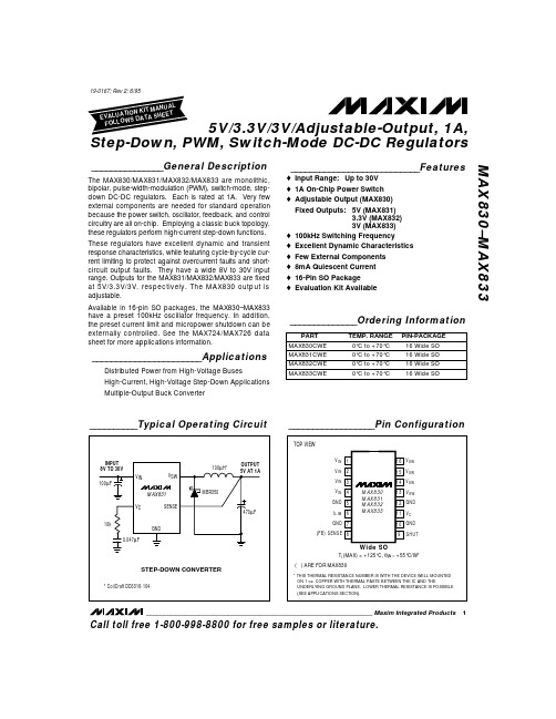
5V/3.3V/3V/Adjustable-Output, 1A, Step-Down, PWM, Switch-Mode DC-DC Regulators MAX830–MAX833
ABSOLUTE MAXIMUM RATINGS
Input Voltage . . . . . . . . . . . . . . . . . . . . . . . . . . . . . . . . . . . . . . . . . . . . . . . . . . 40V Switch Voltage with Respect to Input Voltage. . . . . . . . . . . . . . . . 50V Switch Voltage with Respect to GND (VSW negative) (Note 1). . . . . . . . . . . . . . . . . . . . . . . . . . . . . . . . . . . . . 20V FB/SENSE Voltage . . . . . . . . . . . . . . . . . . . . . . . . . . . . . . . . . . . -0.3V, +10V SHUT Voltage (not to exceed VIN) . . . . . . . . . . . . . . . . . . . . . . . . . . . . 30V Note 1: Do not exceed switch-to-input voltage limitation.
- 1、下载文档前请自行甄别文档内容的完整性,平台不提供额外的编辑、内容补充、找答案等附加服务。
- 2、"仅部分预览"的文档,不可在线预览部分如存在完整性等问题,可反馈申请退款(可完整预览的文档不适用该条件!)。
- 3、如文档侵犯您的权益,请联系客服反馈,我们会尽快为您处理(人工客服工作时间:9:00-18:30)。
General DescriptionThe MAX5933A–MAX5933F/MAX5947A/B/C fully integrat-ed hot-swap controllers for +9V to +80V positive supply rails (MAX5947A/B/C), allow for the safe insertion and removal of circuit cards into live backplanes without caus-ing glitches on the backplane power-supply rail. The MAX5947B is pin- and function-compatible with the LT1641-2. The other devices offer added features such as a choice of active-high or active-low power-good out-puts (PWRGD/PWRGD ), latched/autoretry fault manage-ment, and autoretry duty-cycle options of 3.75% or 0.94%(see the Selector Guide ).The MAX5933A–MAX5933F are available with a default undervoltage lockout threshold of +31V and operate over a supply voltage range of +33V to +80V. The MAX5947A/B/C are available with a default undervoltage of +8.3V. All devices feature a programmable analog foldback current limit. If the device remains in current limit for more than a programmable time, the external n-channel MOSFET is either latched off (MAX5933A/MAX5933C/MAX5947A) or is set to automatically restart after a timeout delay (MAX5933B/MAX5933D/MAX5933E/MAX5933F/MAX5947B/MAX5947C).The MAX5933_ and MAX5947_ operate in the extended temperature range of -40°C to +85°C. These devices are available in an 8-pin SO package.ApplicationsHot Board InsertionElectronic Circuit BreakersIndustrial High-Side Switch/Circuit Breakers Network Routers and Switches 24V/48V Industrial/Alarm SystemsFeatures♦Pin- and Function-Compatible with the LT1641-2(MAX5947B)♦Provides Safe Hot Swap for +9V to +80V Power-Supply Range (MAX5947A/B/C)♦Safe Board Insertion and Removal from Live Backplanes ♦Latched/Autoretry Management♦Active-Low or Active-High Power-Good Output ♦Programmable Foldback Current Limiting ♦High-Side Drive for an External N-Channel MOSFET ♦Built-In Thermal Shutdown ♦Undervoltage Lockout (UVLO)♦Overvoltage Protection♦User-Programmable Supply Voltage Power-Up RateMAX5933A–MAX5933F/MAX5947A/B/CPositive High-Voltage, Hot-Swap Controllers________________________________________________________________Maxim Integrated Products 1Ordering Information19-3263; Rev 1; 7/04For pricing, delivery, and ordering information,please contact Maxim/Dallas Direct!at 1-888-629-4642, or visit Maxim’s website at .Typical Application Circuit and Pin Configuration appear at end of data sheet.*Insert the desired suffix from the Selector Guide into the blank to complete the part number.Selector GuideM A X 5933A –M A X 5933F /M A X 5947A /B /CPositive High-Voltage, Hot-Swap ControllersABSOLUTE MAXIMUM RATINGSELECTRICAL CHARACTERISTICS(V = +24V (MAX5947A/B/C), V = +48V (MAX5933A–MAX5933F), GND = 0V, T = -40°C to +85°C, unless otherwise noted.Stresses beyond those listed under “Absolute Maximum Ratings” may cause permanent damage to the device. These are stress ratings only, and functional operation of the device at these or any other conditions beyond those indicated in the operational sections of the specifications is not implied. Exposure to absolute maximum rating conditions for extended periods may affect device reliability.(Voltages Referenced to GND)V CC .........................................................................-0.3V to +85V SENSE, FB, ON ..........................................-0.3V to (V CC + 0.3V)TIMER, PWRGD, PWRGD .......................................-0.3V to +85V GATE......................................................................-0.3V to +95V Maximum GATE Current....................................-50mA, +150mA Maximum Current into Any Other Pin................................±50mAContinuous Power Dissipation (T A = +70°C)8-Pin SO (derate 5.9mW/°C above +70°C)..................470mW Operating Temperature Range ...........................-40°C to +85°C Maximum Junction Temperature.....................................+150°C Storage Temperature Range.............................-60°C to +150°C Lead Temperature (soldering, 10s).................................+300°C ESD Rating (Human Body Model).. (2000V)MAX5933A–MAX5933F/MAX5947A/B/CPositive High-Voltage, Hot-Swap Controllers_______________________________________________________________________________________3ELECTRICAL CHARACTERISTICS (continued)(V CC = +24V (MAX5947A/B/C), V CC = +48V (MAX5933A–MAX5933F), GND = 0V, T A = -40°C to +85°C, unless otherwise noted.Typical values are at T A = +25°C.) (Note 1)M A X 5933A –M A X 5933F /M A X 5947A /B /CPositive High-Voltage, Hot-Swap Controllers 4_______________________________________________________________________________________Test Circuit and Timing DiagramsFigure 1. Test CircuitFigure 2. ON to GATE TimingFigure 3. FB to PWRGD TimingFigure 4. SENSE to GATE TimingMAX5933A–MAX5933F/MAX5947A/B/CPositive High-Voltage, Hot-Swap Controllers_______________________________________________________________________________________5I CC vs. V CCV CC (V)I C C (m A )0.30.60.91.21.51.82.12.42.7072645648403380I CC vs. TEMPERATURETEMPERATURE (°C)I C C (m A )603510-150.51.01.52.02.53.00-4085FB LOW-VOLTAGE THRESHOLDvs. TEMPERATUREM A X 5933 t o c 03TEMPERATURE (°C)F B L O W -V O L T AG E TH R E S H O L D (V )603510-151.2051.2101.2151.2201.2251.2301.2351.2401.2451.2501.200-4085FB HIGH-VOLTAGE THRESHOLDvs. TEMPERATUREM A X 5933 t o c 04TEMPERATURE (°C)F B H I G H -V O L T A G E T H R E S H O L D (V )603510-15-40851.2851.2901.2951.3001.3051.3101.3151.3201.3251.3301.3351.280FB HYSTERESIS vs. TEMPERATUREM A X 5933 t o c 05TEMPERATURE (°C)F B H Y S T E R E S I S (V )603510-150.050.060.070.080.090.100.110.04-4085I GATE PULLUP CURRENT vs. TEMPERATURETEMPERATURE (°C)I G A T E P U L L U P C U R R E N T (µA )6035-1510-12-11-10-9-7-8-6-5-13-4085MAX5947_GATE DRIVE vs. V CCM A X 5933 t o c 08V CC (V)G A T E D R I V E (V G A T E - V C C ) (V )605070402030102468101214160080GATE DRIVE vs. TEMPERATURETEMPERATURE (°C)G A T E D R I V E (V G A T E - V C C ) (V )603510-1567891011121314155-4085Typical Operating Characteristics(V CC = +48V, T A = +25°C, unless otherwise noted.)M A X 5933A –M A X 5933F /M A X 5947A /B /CPositive High-Voltage, Hot-Swap Controllers 6_______________________________________________________________________________________Typical Operating Characteristics (continued)(V CC = +48V, T A = +25°C, unless otherwise noted.)TIMER PULLUP CURRENT vs. TEMPERATUREM A X 5933 t o c 09TEMPERATURE (°C)T I M E R P U L L U P C U R R E N T (µA )603510-15-85-80-75-70-65-60-90-4085MAX5933_TIMER PULLUP CURRENT vs. V CCV CC (V)T I M E R P U L L U P C U R R E N T (µA )-78-77-76-75-74-73-79405060703080MAX5947_TIMER PULLUP CURRENT vs. V CCV CC (V)T I M E R P U L L U P C U R R E N T (µA )70605040302010-78-77-76-75-74-73-79080ON HIGH-VOLTAGE THRESHOLDvs. TEMPERATUREM A X 5933 t o c 12TEMPERATURE (°C)O N H I G H -V O L T A G E T H R E S H O L D (V )603510-151.2931.3031.3131.3231.3331.3431.283-4085ON LOW-VOLTAGE THRESHOLDvs. TEMPERATUREM A X 5933 t o c 13TEMPERATURE (°C)O N L O W -V O L T A G E T H R E S H O L D (V )603510-151.2151.2251.2351.2451.2551.2651.205-4085ON HYSTERESIS vs. TEMPERATUREM A X 5933 t o c 14TEMPERATURE (°C)O N H Y S T E R E S I S (V )603510-150.0750.0770.0790.0810.0830.073-4085SENSE REGULATION VOLTAGE vs. V FBM A X 5933 t o c 16V FB (V)S E N S E R E G U L A T I O N V O L T A G E (m V )0.80.60.40.251015202530354045500 1.0PWRGD V OUT LOW vs. I LOADI LOAD (mA)P W R G D V O U T L O W (V )705030246810121416182001090MAX5933A–MAX5933F/MAX5947A/B/CPositive High-Voltage, Hot-Swap Controllers_______________________________________________________________________________________7M A X 5933A –M A X 5933F /M A X 5947A /B /CPositive High-Voltage, Hot-Swap ControllersFunctional DiagramMAX5933A–MAX5933F/MAX5947A/B/CPositive High-Voltage, Hot-Swap Controllers_______________________________________________________________________________________9Detailed DescriptionThe MAX5933_ and MAX5947_ are fully integrated hot-swap controllers for positive supply rails. The devices allow for the safe insertion and removal of circuit cards into live backplanes without causing glitches on the backplane power-supply rail. During startup, the MAX5933_ and MAX5947_act as current regulators using an external sense resistor and a MOSFET to limit the amount of current drawn by the load.The MAX5933_ operate from a +33V to +80V supply voltage range and have a default undervoltage lockout (UVLO) set to +31V. The MAX5947_ operate from a +9V to +80V supply voltage range and have a default UVLO set to +8.3V. The UVLO threshold is adjustable using a resistive divider connected from V CC to ON to GND (see Figure 5).The MAX5933_ and MAX5947_ monitor the input volt-age, the output voltage, the output current, and the die temperature. These devices feature power-good outputs (PWRGD/PWRGD ) to indicate the status of the output voltage by monitoring the voltage at FB (see the Power-Good Detection section).As shown in Figure 5, a sense resistor is connected between V CC and SENSE to regulate the voltage across the sense resistor (V IN - V SENSE ) to 47mV when the voltage at FB ≥0.5V. The current-limit threshold (V SENSETRIP ) decreases linearly from 47mV to 12mV as FB decreases from 0.5V to 0V.An undervoltage fault is detected when ON goes below the threshold (V ONL = 1.233V) and the voltage at GATE goes low as a result to turn off the MOSFET. ON must pass the V ONH = 1.313V threshold to turn on the MOSFET again.Figure 5. Application CircuitM A X 5933A –M A X 5933F /M A X 5947A /B /CPositive High-Voltage, Hot-Swap Controllers 10______________________________________________________________________________________Applications InformationHot-Circuit InsertionWhen circuit boards are inserted into a live backplane,the supply bypass capacitors on the boards draw high peak currents from the backplane power bus as they charge up. The transient currents can permanently damage the connector pins and glitch the system sup-ply, causing other boards in the system to reset.Power-Up SequenceThe power supply on a board is controlled by placing an external n-channel MOSFET (Q1) in the power path (Figure 5). Resistor R SENSE provides current detection and capacitor C1 provides control of the GATE slew rate. Resistor R6 provides current control-loop compen-sation, while R5 prevents high-frequency oscillations in Q1. Resistors R1 and R2 provide undervoltage sensing.After the power pins first make contact, transistor Q1 is turned off. When the voltage at ON exceeds the turn-on threshold voltage, the voltage on V CC exceeds the undervoltage lockout threshold, and when the voltage on TI MER is less than 1.233V, transistor Q1 turns on (Figure 6).The voltage at GATE rises with a slope equal to 10µA/C1 and the supply inrush current is set at:I INRUSH = C L x 10µA/C1When the voltage across the current-sense resistor R SENSE reaches V SENSETRIP , the inrush current is limit-ed by the internal current-limit circuitry that adjusts the voltage on GATE to maintain a constant voltage across the sense resistor.Once the voltage at the output has reached its final value,as sensed by resistors R3 and R4, PWRGD goes high or PWRGD goes low.Short-Circuit ProtectionThe MAX5933_/MAX5947_ feature a programmable fold-back current limit with an electronic circuit breaker that protects against short circuits or excessive supply cur-rents. The current limit is set by placing a sense resistor between V CC (pin 8) and SENSE (pin 7).To prevent excessive power dissipation in the pass transistor and to prevent voltage spikes on the input supply during short-circuit conditions at the output, the current folds back as a function of the output voltage that is sensed at FB (Figure 7).When the voltage at FB is 0V, the current-limit circuit drives GATE to force a constant 12mV drop across the sense resistor. As the output voltage at FB increases,the voltage across the sense resistor increases until FB reaches 0.5V. At this point, the voltage across the sense resistor is held constant at 47mV.The maximum current limit is calculated as:I LIMIT = 47mV / R SENSEFor a 0.025Ωsense resistor, the current limit is set at 1.88A and folds back to 480mA when the output is shorted to ground.The MAX5933_/MAX5947_also feature a variable over-current response time. The time required to regulate Q1’s drain current depends on:1)Q1’s input capacitance2)GATE capacitor C1 and compensation resistor R63)The internal delay from SENSE to GATEFigure 8 shows the delay from a voltage step at SENSE until GATE voltage starts falling, as a function of overdrive.20ms/divFigure 6. Power-Up Waveforms Figure 7. Current-Limit Sense Voltage vs. Feedback VoltageTIMER TI MER provides a method for programming the maxi-mum time the device is allowed to operate in current limit. When the current-limit circuitry is not active, TIMER is pulled to GND by a 3µA current source. After the current-limit circuit becomes active, an 80µA pullup current source is connected to TIMER, and the voltage rises with a slope equal to 77µA/C TIMER, as long as the current-limit circuit remains active. Once the desired maximum current-limit time is chosen, the capacitor value is:C(nF) = 65 x t(ms)orT LIMIT= (C TIMER/80µA) x 1.233VWhen the current-limit circuit turns off, TI MER is dis-charged to GND by the 3µA current source. Whenever TI MER reaches 1.233V, the internal fault latch is set. GATE is immediately pulled to GND and TI MER is pulled back to GND by the 3µA current source. When TIMER falls below 0.5V, ON is pulsed low to reset the internal fault latch.The waveform in Figure9 shows how the output latches off following a short circuit. The drop across the sense resistor is held at 12mV as the timer ramps up. Since the output did not rise, FB remains below 0.5V and the circuit latches off. For Figure9, C T= 100nF.Undervoltage and Overvoltage Detection ON can be used to detect an undervoltage condition at the power-supply input. ON is internally connected to an analog comparator with 80mV of hysteresis. I f ON falls below its threshold voltage (1.233V), GATE is pulled low and is held low until ON is high again.Figure10 shows an overvoltage detection circuit. When the input voltage exceeds the Zener diode’s breakdown voltage, D1 turns on and starts to pull TIMER high. After TIMER is pulled higher than 1.233V, the fault latch is set and GATE is pulled to GND immediately, turning off transistor Q1 (see Figure11). Operation is restored either by interrupting power or by pulsing ON low.Power-Good Detection The MAX5933_/MAX5947_ include a comparator for mon-itoring the output voltage. The noninverting input (FB) is compared against an internal 1.233V precision reference and exhibits 80mV hysteresis. The comparator’s output (PWRGD) is open drain and capable of operating from a pullup as high as 80V. The PWRGD is similar to PWRGD with an opposite polarity (active low) output.The PWRGD (PWRGD) can be used to directly enable/disable a power module with an active-high enable input. Figure12 shows how to use PWRGD to control an active-low enable-input power module. Signal inversion is accomplished by transistor Q2 and R7.Supply Transient Protection The MAX5933_/MAX5947_are 100% tested and guar-anteed to be safe from damage with supply voltages up to 80V. However, spikes above 85V may damage the device. During a short-circuit condition, the large change in currents flowing through the power-supply traces can cause inductive voltage spikes which could exceed 85V. To minimize the spikes, the power-trace parasitic inductance should be minimized by using wider traces or heavier trace plating and a 0.1µF bypass capacitor placed between V CC and GND. A transient voltage suppressor (TVS) at the input can also prevent damage from voltage surges.Figure8. Response Time to Overcurrent10ms/divFigure9. Short-Circuit WaveformsMAX5933A–MAX5933F/MAX5947A/B/C______________________________________________________________________________________11GATE VoltageA curve of Gate Drive vs. V CC is shown in Figure 13.GATE is clamped to a maximum voltage of 18V above the input voltage. At a minimum input-supply voltage of 33V,the minimum gate drive voltage is 10V. When the input supply voltage is higher than 20V, the gate-drive voltage is at least 10V and a standard n-channel MOSFET can be used. Using the MAX5947 in applications over a 9V to 20V range, a logic-level N-FET must be used with a prop-er protection Zener diode between its gate and source (see D1 in Figure 5).Thermal ShutdownI f the MAX5933_/MAX5947_ die temperature reaches +150°C, an overtemperature fault is generated. As a result, GATE goes low and turns the external MOSFET off.The MAX5933_/MAX5947_ die temperature must cool down below +130°C before the overtemperature fault condition is removed.M A X 5933A –M A X 5933F /M A X 5947A /B /C12______________________________________________________________________________________10µs/div11. Overvoltage Waveforms Figure 10. Overvoltage DetectionMAX5933A–MAX5933F/MAX5947A/B/C13Layout ConsiderationsTo achieve accurate current sensing, a Kelvin connec-tion is recommended. The minimum trace width for 1oz copper foil is 0.02in per amplifier to ensure the trace stays at a reasonable temperature. However, 0.03in.per amplifier or wider is recommended. Note that 1oz copper exhibits a sheet resistance of approximately 530µΩ/square. Small resistances add up quickly in high-current applications. To improve noise immunity,connect the resistor-divider to ON close to the device,and keep traces to V CC and GND short. A 0.1µF capacitor from ON to GND also helps reject induced noise. Figure 14 shows a layout that addresses these issues. I t is recommended that 2oz copper is used,particularly as the external MOSFET must be thermally coupled to the MAX5933_/MAX5947_ to ensure proper thermal-shutdown operation.Figure 12. Active-Low Enable ModuleTypical Application CircuitM A X 5933A –M A X 5933F /M A X 5947A /B /CChip InformationTRANSISTOR COUNT: 1573PROCESS: BiCMOSFigure 14. Recommended Layout for R1, R2, and R SENSEPin ConfigurationMaxim cannot assume responsibility for use of any circuitry other than circuitry entirely embodied in a Maxim product. No circuit patent licenses are implied. Maxim reserves the right to change the circuitry and specifications without notice at any time.Maxim Integrated Products, 120 San Gabriel Drive, Sunnyvale, CA 94086 408-737-7600 ____________________15©2004 Maxim Integrated Products Printed USAis a registered trademark of Maxim Integrated Products.Package Information(The package drawing(s) in this data sheet may not reflect the most current specifications. For the latest package outline informationgo to /packages.)MAX5933A–MAX5933F/MAX5947A/B/C。