SI1058X-T1-GE3中文资料
SI2301CDS-T1-GE3中文资料

Vishay SiliconixSi2301CDSP-Channel 20-V (D-S) MOSFET FEATURES•Halogen-free Option Available•TrenchFET ® Power MOSFETAPPLICATIONS •Load SwitchMOSFET PRODUCT SUMMARYV DS (V)R DS(on) (Ω)I D (A)a Q g (Typ.)- 200.112 at V GS = - 4.5 V - 3.1 3.3 nC0.142 at V GS = - 2.5 V- 2.7Notes:a. Based on T C = 25 °C.b. Surface Mounted on 1" x 1" FR4 board.c. t = 5 s.d. Maximum under Steady State conditions is 175 °C/W.ABSOLUTE MAXIMUM RATINGS T A = 25°C, unless otherwise notedParameter Symbol Limit U nitDrain-Source Voltage V DS - 20VGate-Source Voltage V GS ± 8Continuous Drain Current (T J = 150 °C)T C = 25 °C I D- 3.1A T C = 70 °C - 2.5T A = 25 °C - 2.3b, c T A = 70 °C - 1.8b, cPulsed Drain Current I DM - 10Continuous Source-Drain Diode CurrentT C = 25 °C I S - 1.3T A = 25 °C - 0.72b, c Maximum Power Dissipation T C = 25 °C P D 1.6WT C = 70 °C 1.0T A = 25 °C 0.86b, c T A = 70 °C 0.55b, cOperating Junction and Storage T emperature Range T J , T stg - 55 to 150°C THERMAL RESISTANCE RATINGSParameter Symbol Typical Maximum UnitMaximum Junction-to-Ambient b, d ≤ 5 s R thJA 120145°C/WMaximum Junction-to-Foot (Drain)Steady State R thJF 6278Vishay SiliconixSi2301CDSNotes:a. Pulse test; pulse width ≤ 300 µs, duty cycle ≤ 2 %.b. Guaranteed by design, not subject to production testing.Stresses beyond those listed under “Absolute Maximum Ratings” may cause permanent damage to the device. These are stress ratings only, and functional operation of the device at these or any other conditions beyond those indicated in the operational sections of the specifications is not implied. Exposure to absolute maximum rating conditions for extended periods may affect device reliability.MOSFET SPECIFICATIONS T J = 25°C, unless otherwise notedParameter Symbol Test Conditions Min.Typ.Max.U nit StaticDrain-Source Breakdown Voltage V DS V DS = 0 V, I D = - 250 µA- 20VV DS Temperature Coefficient ΔV DS /T J I D = - 250 µA - 18mV/°C V GS(th) T emperature Coefficient ΔV GS(th)/T J 2.2Gate-Source Threshold Voltage V GS(th) V DS = V GS , I D = - 250 µA - 0.4- 1V Gate-Source LeakageI GSS V DS = 0 V , V GS = ± 8 V ± 100nA Zero Gate Voltage Drain Current I DSS V DS = - 20 V , V GS = 0 V - 1µA V DS = - 20 V, V GS = 0 V , T J = 55 °C- 10On-State Drain Current aI D(on) V DS ≤ - 5 V , V GS = - 4.5 V - 6A Drain-Source On-State Resistance aR DS(on) V GS = - 4.5 V, I D = - 2.8 A 0.0900.112ΩV GS = - 2.5 V, I D = - 2.0 A 0.1100.142Forward T ransconductance a g fsV DS = - 5 V , I D = - 2.8 A2.0SDynamic bInput Capacitance C iss V DS = - 10 V , V GS = 0 V , f = 1 MHz405pFOutput CapacitanceC oss 75Reverse Transfer Capacitance C rss 55Total Gate Charge Q g V DS = - 10 V , V GS = - 4.5 V , ID = - 3 A 5.510nC V DS = - 10 V , V GS = - 2.5 V , I D = - 3 A 3.36Gate-Source Charge Q gs 0.7Gate-Drain Charge Q gd 1.3Gate Resistance R g f = 1 MHz6.0ΩTurn-On Delay Time t d(on) V DD = - 10 V, R L = 10 ΩI D = - 1 A, V GEN = - 4.5 V , R G = 1 Ω1120ns Rise Timet r 3560Turn-Off Delay Time t d(off) 3050Fall Timet f1020Drain-Source Body Diode Characteristics Continuous Source-Drain Diode Current I S T C = 25 °C- 1.3A Pulse Diode Forward Current a I SM - 10Body Diode VoltageV SD I S = - 0.7 A- 0.8- 1.2V Body Diode Reverse Recovery Time t rr I F = - 3.0 A, dI/dt = 100 A/µs, T J = 25 °C3050ns Body Diode Reverse Recovery Charge Q rr 2550nC Reverse Recovery Fall Time t a 15nsReverse Recovery Rise Timet b15Output CharacteristicsOn-Resistance vs. Drain Current and Gate VoltageTransfer CharacteristicsCapacitanceOn-Resistance vs. Junction TemperatureThreshold VoltageSingle Pulse PowerVishay SiliconixSi2301CDSTYPICAL CHARACTERISTICS 25°C, unless otherwise notedVishay Siliconix maintains worldwide manufacturing capability. Products may be manufactured at one of several qualified locations. Reliability data for Silicon Technology and Package Reliability represent a composite of all qualified locations. For related documents such as package/tape drawings, part marking, and reliability data, see /ppg?68741.Normalized Thermal Transient Impedance, Junction-to-FootDisclaimer Legal Disclaimer NoticeVishayAll product specifications and data are subject to change without notice.Vishay Intertechnology, Inc., its affiliates, agents, and employees, and all persons acting on its or their behalf (collectively, “Vishay”), disclaim any and all liability for any errors, inaccuracies or incompleteness contained herein or in any other disclosure relating to any product.Vishay disclaims any and all liability arising out of the use or application of any product described herein or of any information provided herein to the maximum extent permitted by law. The product specifications do not expand or otherwise modify Vishay’s terms and conditions of purchase, including but not limited to the warranty expressed therein, which apply to these products.No license, express or implied, by estoppel or otherwise, to any intellectual property rights is granted by this document or by any conduct of Vishay.The products shown herein are not designed for use in medical, life-saving, or life-sustaining applications unless otherwise expressly indicated. Customers using or selling Vishay products not expressly indicated for use in such applications do so entirely at their own risk and agree to fully indemnify Vishay for any damages arising or resulting from such use or sale. Please contact authorized Vishay personnel to obtain written terms and conditions regarding products designed for such applications.Product names and markings noted herein may be trademarks of their respective owners.元器件交易网。
SIC762CD-T1-GE3;中文规格书,Datasheet资料

Integrated DrMOS Power StageDESCRIPTIONThe SiC762CD is an integrated solution that contains PWM optimized n-channel MOSFETs (high side and low side) and a full featured MOSFET driver IC. The device complies with the Intel DrMOS standard for desktop and server V core power stages. The SiC762CD delivers up to 35 A continuous output current and operates from an input voltage range of 3 V to 27 V. The integrated MOSFETs are optimized for output voltages in the ranges of 0.8 V to 2.0 V with a nominal input voltage of 24 V. The device can also deliver very high power at 5 V output for ASIC applications.The SiC762CD incorporates an advanced MOSFET gate driver IC. This IC accepts a single PWM input from the V R controller and converts it into the high side and low side MOSFET gate drive signals. The driver IC is designed to implement the skip mode (SMOD) function for light load efficiency improvement. Adaptive dead time control also works to improve efficiency at all load points. The SiC762CD has a thermal warning (THDN) that alerts the system of excessive junction temperature. The driver IC includes an enable pin, UVLO and shoot through protection.The SiC762CD is optimized for high frequency buck applications. Operating frequencies in excess of 1 MHz can easily be achieved.The SiC762CD is packaged in Vishay Siliconix high performance PowerP AK MLP6 x 6 package. Compact co-packaging of components helps to reduce stray inductance, and hence increases efficiency. •FEATURES•Integrated Gen III MOSFETs and DrMOScompliant gate driver IC•Enables V core switching at 1 MHz•Easily achieve > 90 % efficiency in multi-phase, low output voltage solutions•Low ringing on the VSWH pin reduces EMI•Pin compatible with DrMOS 6 x 6 version 3.0•Tri-state PWM input function prevents negative output voltage swing• 5 V logic levels on PWM•MOSFET threshold voltage optimized for 5 V driver bias supply•Automatic skip mode operation (SMOD) for light load efficiency•Under-voltage lockout•Built-in bootstrap schottky diode•Adaptive deadtime and shoot through protection •Thermal shutdown warning flag•Low profile, thermally enhanced PowerPAK® MLP 6 x 640 pin package•Halogen-free according to IEC 61249-2-21 definition •Compliant to RoHS directive 2002/95/ECAPPLICATIONS•CPU and GPU core voltage regulation•Server, computer, workstation, game console, graphics boards, PCSIC762CD APPLICATION DIAGRAMMa.T A = 25 °C and all voltages referenced to P GND = C GND unless otherwise noted.Stresses beyond those listed under "Absolute Maximum Ratings" may cause permanent damage to the device. These are stress ratings only,and functional operation of the device at these or any other conditions beyond those indicated in the operational sections of the specifications is not implied. Exposure to absolute maximum rating/conditions for extended periods may affect device reliability.Note:a.Recommended operating conditions are specified over the entire temperature range, and all voltages referenced to P GND = C GND unless otherwise noted.ORDERING INFORMATIONPart Number Package SiC762CD-T1-GE3PowerPAK MLP66-40SiC762DBReference boardRECOMMENDED OPERATING CONDITIONSParameter Symbol Min.Typ.Max.UnitInput Voltage V IN 3.01224VControl Input Voltage V CIN 4.5 5.5Drive Input Voltage V DRV 4.55.5Switch NodeV SW_DC1224THERMAL RESISTANCE RATINGSParameterSymbol Typ.Max.Unit Maximum Power Dissipation at T PCB = 25 °C P D_25C 25W Maximum Power Dissipation at T PCB = 100 °C P D_100C 10Thermal Resistance from Junction to T op R th_J_TOP 15°C/WThermal Resistance from Junction to PCBR th_J_PCB5Notes:a.Typical limits are established by characterization and are not production tested.b.Guaranteed by design.ELECTRICAL SPECIFICATIONSParameter Symbol Test Conditions Unless SpecifiedV DSBL# = V SMOD = 5 V ,V IN = 12 V , V VDRV = V VCIN = 5 V ,T A = 25 °C Min.Typ.a Max.UnitPower SuppliesV CIN Control Input Current I VCIN V DSBL# = 0 V , no switching21µAV DSBL# = 5 V , no switching 350V DSBL# = 5 V , f s = 300 kHz, D = 0.1500Drive Input Current (Dynamic)I VDRV f s = 300 kHz, D = 0.11418mAf s = 1000 kHz, D = 0.14054Bootstrap SupplyBootstrap Switch Forward Voltage V BS Diode V VCIN = 5 V, forward bias current 2 mA0.600.75VControl Inputs (PWM, DSBL#, SMOD)PWM Rising Threshold V th_pwm_r 3.5 3.9 4.2VPWM Falling Threshold V th_pwm_f 0.8 1.0 1.2PWM T ristate Rising Threshold V th_tri_r 0.9 1.3 1.8PWM T ristate Falling ThresholdV th_tri_f 3.43.74.0PWM T ristate Rising Threshold Hysteresis V hys_tri_r 280mV PWM T ristate Falling Threshold Hysteresis V hys_tri_f 180T ristate Hold-Off Time b t TSHO 150ns PWM Input CurrentI PWM V PWM = 5 V 250µA V PWM = 0 V - 250SMOD, DSBL# Logic Input Voltage V LOGIC_LH Rising (low to high) 2.0V V LOGIC_LH Falling (high to low)0.8Pull Down Impedance R THDN 5 k Ω resistor pull-up to V CIN40ΩTHDN Output Low V THDNL0.04V ProtectionThermal Warning Flag Set 150°CThermal Warning Flag Clear 135Thermal Warning Flag Hysteresis 15Under Voltage Lockout V CIN V UVLO Rising, on threshold 3.3 3.9V Under Voltage Lockout V CINFalling, off threshold 2.32.95Under Voltage Lockout Hysteresis V CIN V UVLO_HYST 400mV High Side Gate Discharge ResistorbR HS_DSCRGV VDRV = V VCIN = 0 V; V IN = 12 V20.2k ΩNote:a. Min. and Max. are not 100 % production tested.TIMING DEFINITIONSNote:GH is referenced to the high side source. GL is referenced to the low side source.TIMING SPECIFICATIONSParameter Symbol Test Conditions Unless Specified V VDRV = V VCIN = V DSBL# = 5 V ,V VIN = 12 V , T A = 25 °C Min. Typ.Max.UnitTurn Off Propagation DelayHigh Side at d_off_HS 25 % of PWM to 90 % of GH102035nsRise Time High Side t r_HS 10 % to 90 % of GH 10Fall Time High Side t f_HS 90 % to 10 % of GH 8Turn Off Propagation Delay Low Side at d_off_LS 75 % of PWM to 90 % of GL103745Rise Time Low Side t r_LS 10 % to 90 % of GL 6Fall Time Low Side t f_LS 90 % to 10 % of GL 5Dead Time Rising t dead_on 10 % of GL to 10 % of GH 27Dead Time Fallingt dead_off10 % of GH to 10 % of GL19Region DefinitionSymbol 1T urn off propagation delay LSt d_off_LS 2Fall time LS t f_LS 3Dead time rising t dead_on 4Rise time HSt r_HS 5T urn off propagation delay HSt d_off_HS 6Fall time HS t f_HS 7Dead time falling t dead_off 8Rise time LSt r_LSP W MGHGLS W1234 567810%90%10%90%75%25%SIC762CD BLOCK DIAGRAMDETAILED OPERATIONAL DESCRIPTIONPWM Input with Tristate FunctionThe PWM input receives the PWM control signal from the V R controller IC. The PWM input is designed to be compatible with standard controllers using two state logic (H and L) and advanced controllers that incorporate Tristate logic (H, L and Tristate) on the PWM output. For two state logic, the PWM input operates as follows. When PWM is driven above V th_pwm_r the low side is turned off and the high side is turned on. When PWM input is driven below V th_pwm_f the high side turns off and the Low side turns on. For Tristate logic, the PWM input operates as above for driving the MOSFETs.However, there is an third state that is entered into as the PWM output of Tristate compatible controller enters its high impedance state during shut-down. The high impedance state of the controller's PWM output allows the SiC762CD to pull the PWM input into the Tristate region (see the Tristate Voltage Threshold Diagram below). If the PWM input stays in this region for the Tristate Hold-Off Period, t TSHO , both high side and low side MOSFETs are turned off. This function allows the V R phase to be disabled without negative output voltage swing caused by inductor ringing and saves a Schottky diode clamp. The PWM and Tristate regions are separated by hysteresis to prevent false triggering. The SiC762CD incorporates PWM voltage thresholds that are compatible with 5 V logic.Disable (DSBL#)In the low state, the DSBL# pin shuts down the driver IC and disables both high-side and low-side MOSFET. In this state,the standby current is minimized. If DSBL# is left unconnected an internal pull-down resistor will pull the pin Diode Emulation Mode (SMOD) Skip ModeWhen SMOD pin is low the diode emulation mode is enabled.This is a non-synchronous conversion mode that improves light load efficiency by reducing switching losses. Conducted losses that occur in synchronous buck regulators when inductor current is negative are also reduced. Circuitry in the gate drive IC detects when inductor current crosses zero and automatically stops switching the low side MOSFET. See SMOD Operation Diagram for additional details. This function can also be used for a pre-biased output voltage. If SMOD is left unconnected, an internal pull up resistor will pull the pin up to V CIN (Logic High) to disable the diode emulation function.Thermal Shutdown Warning (THDN)The THDN pin is an open drain signal that flags the presence of excessive junction temperature. Connect a maximum of 20 k Ω to pull this pin up to V CIN . An internal temperature sensor detects the junction temperature. The temperature threshold is 150 °C. When this junction temperature is exceeded the THDN flag is set. When the junction temperature drops below 135 °C the device will clear the THDN signal. The SiC762CD does not stop operation when the flag is set. The decision to shutdown must be made by an external thermal control function.Voltage Input (V IN )This is the power input to the drain of the high-side Power MOSFET. This pin is connected to the high power intermediate BUS rail.Switch Node (V SWH and PHASE)The Switch node V SWH is the circuit PWM regulated output.Figure 2U V LOV DR VGHGLC G N DP G N DV S W HBOOTV I N V CI NP W MDSBL#THD NSMOD Thermal W arningT ristate P W MAST C N TL DCM DETECTPHASEregulated high output for the buck converter. The PHASE pin is internally connected to the switch node V SWH . This pin is to be used exclusively as the return pin for the BOOT capacitor. A 20.2 k Ω resistor is connected between GH and PHASE to provide a discharge path for the HS MOSFET in the event that V CIN goes to zero while V IN is still applied.Ground connections (C GND and P GND )P GND (power ground) should be externally connected to C GND (control signal ground). The layout of the Printed Circuit Board should be such that the inductance separating the C GND and P GND should be a minimum. Transient differences due to inductance effects between these two pins should not exceed 0.5 V.Control and Drive Supply Voltage Input (V DRV ,V CIN )V CIN is the bias supply for the gate drive control IC. V DRV is the bias supply for the gate drivers. It is recommended to separate these pins through a resistor. This creates a low pass filtering effect to avoid coupling of high frequency gate drive noise into the IC.Bootstrap Circuit (BOOT)The internal bootstrap switch and an external bootstrap capacitor form a charge pump that supplies voltage to the BOOT pin. An integrated bootstrap diode is incorporated so that only an external capacitor is necessary to complete the bootstrap circuit. Connect a boot strap capacitor with one leg tied to BOOT pin and the other tied to PHASE pin.Shoot-Through Protection and Adaptive Dead Time (AST)The SiC762CD has an internal adaptive logic to avoid shoot through and optimize dead time. The shoot through protection ensures that both high-side and low-side MOSFET are not turned on the same time. The adaptive dead time control operates as follows. When PWM input goes high the LS gate starts to go low after a few ns. When this signal crosses through 1.7 V the logic to switch the HS gate on is activated. When PWM goes low the HS gate goes low. When the HS gate-to-source drive signal crosses through 1.7 V the logic to turn on the LS gate is activated.This feature helps to adjust dead time as gate transitions change with respect to output current and temperature.Under Voltage Lockout (UVLO)During the start up cycle, the UVLO disables the gate drive holding high-side and low-side MOSFET gate low until the input voltage rail has reached a point at which the logic circuitry can be safely activated. The SiC762CD also incorporates logic to clamp the gate drive signals to zero when the UVLO falling edge triggers the shutdown of the device. As an added precaution, a 20.2 k Ω resistor is connected between GH and PHASE to provide a discharge path for the HS MOSFET.TRISTATE PWM VOLTAGE THRESHOLD DIAGRAMDEVICE TRUTH TABLEDSBL#SMOD PWM GH GL Open X X L L L X X L L H L L L H (I L > 0), L (I L ≤ 0)H L H H L H H H H L HHLLHFigure 3V th_tri_f V th_p w m_r V th_tri_rV th_p w m_fP W MGHGL t TSHOt TSHOSMOD OPERATION DIAGRAMPIN CONFIGURATIONFigure 4DSBLSMODP W MGHGLV S WI L > 0I L = 0t d(O N)t d(OFF)Figure 5 - PowerPAK MLP 6 x 6 40P Pin Out - Top ViewV I NP2A G N DP1V S W HP330V S W H29V S W H28 P G N D27 P G N D26 P G N D25 P G N D24 P G N D23 P G N D22 P G N D21 P G N D4PWM39DSBL#38THDN37CGND36GL35VSWH34VSWH33VSWH32VSWH31VSWHSMOD 1V CI N 2V DR V 3BOOT 4C G ND 5GH 6PHASE 7V I N8V I N 9V I N 1020 PGND19 PGND18PGND17 PGND16 PGND15VSWH14VIN13VIN12VIN11VINPIN DESCRIPTIONPin Number Symbol Description1SMOD Disable low side gate operation. Active low.2V CIN This will be the bias supply input for control IC (5 V).3V DRV IC bias supply and gate drive supply voltage (5 V).4BOOT High side driver bootstrap voltage pin for external bootstrap capacitor.5, 37, PAD1C GND Control signal ground. It should be connected to P GND externally. All pins internally connected.6GH Gate signal output pin for high side MOSFET. Pin for monitoring.7PHASE Return pin for the HS bootstrap capacitor. Connect a 0.1 µF ceramic capacitor from this pin to the boot pin (4).8 to 14, PAD2V IN Input voltage for power stage. It is the drain of the high-side MOSFET.15, 29 to 35,PAD3VSWHIt is the phase node between high side MOSFET source and low side MOSFET drain. It should be connected to an output inductor. All pins internally connected.16 to 28P GND Power ground.36GL Gate signal output pin for low side MOSFET. Pin for monitoring.38THDN Thermal shutdown open drain output. Use a 10K pull up resistor to V CIN.39DSBL#Disable pin. Active low.ELECTRICAL CHARACTERISTICSI CIN (mA) vs. Temperature at Frequency = 300 kHzD = 10 %, V CIN = V DRV = 5 VPWM Falling Threshold (V) vs. Temperature (°C)V CIN = V DRV = 5 VDSBL Falling Threshold (V) vs. Temperature (°C)I DRV (mA) vs. Temperature at Frequency = 300 kHzD = 10 %, V CIN = V DRV = 5 VPWM Rising Threshold (V) vs. Temperature (°C)V CIN = V DRV = 5 VDSBL Rising Threshold (V) vs. Temperature (°C)ELECTRICAL CHARACTERISTICSSMOD Falling Threshold (V) vs. Temperature (°C)V CIN = V DRV = 5 VI CIN + I DRV (mA) vs. Temperature at Frequency = 1 MHzD = 10 %, V CIN = V DRV = 5 VPWM Falling Tristate (V) vs. Temperature (°C)SMOD Rising Threshold (V) vs. Temperature (°C)V CIN = V DRV = 5 VI DRV (mA) vs. Temperature at Frequency = 1 MHzD = 10 %, V CIN = V DRV = 5 VPWM Rising Tristate Threshold (V) vs. Temperature (°C)ELECTRICAL CHARACTERISTICSCINSMOD Falling Threshold vs. V CINPWM Falling Threshold vs. VCINSMOD Rising Threshold vs. V CINPWM Rising Threshold vs. V分销商库存信息: VISHAYSIC762CD-T1-GE3。
维沙伊 Siliconix Si5424DC 数据手册说明书

SI5424DC-T1-GE3Vishay SiliconixSi5424DCN-Channel 30 V (D-S) MOSFETFEATURES•TrenchFET ® Power MOSFET •Material categorization:or definitions of compliance please see /doc?99912APPLICATIONS•Load Switch- Notebook PCNotes:a.Package limited.b.Surface mounted on 1” x 1” FR4 board.c.t = 5 s.d.See solder profile (/doc?73257). The ChipFET 1206-8 is a leadless package. The end of the lead terminal is exposed copper (not plated) as a result of the singulation process in manufacturing. A solder fillet at the exposed copper tip cannot be guaranteed and is not required to ensure adequate bottom side solder interconnection.e.Rework Conditions: manual soldering with a soldering iron is not recommended for leadless components.f.Maximum under steady state conditions is 80 °C/W. PRODUCT SUMMARYV DS (V)R DS(on) (Ω)I D (A)aQ g (Typ.)300.024 at V GS = 10 V 611 nC0.030 at V GS = 4.5 V6ABSOLUTE MAXIMUM RATINGS (T A = 25 °C, unless otherwise noted)Parameter Symbol Limit UnitDrain-Source Voltage V DS 30VGate-Source VoltageV GS ± 25Continuous Drain Current (T J = 150 °C)T C = 25 °C I D 6a AT C = 70 °C 6aT A = 25 °C 6a T A = 70 °C 6aPulsed Drain Current I DM 40Continuous Source-Drain Diode CurrentT C = 25 °C I S 5.2aT A = 25 °C 2.1b, cSingle Pulse Avalanche Current L = 0.1 mHI AS 16Avalanche Energy E AS 12.8mJMaximum Power Dissipation aT C = 25 °C P D 6.25W T C = 70 °C 4T A = 25 °C 2.5b, c T A = 70 °C 1.6b, cOperating Junction and Storage T emperature Range T J , T stg - 55 to 150°CSoldering Recommendations (Peak Temperature)d, e260THERMAL RESISTANCE RATINGSParameter Symbol Typical Maximum UnitMaximum Junction-to-Ambientb, f t ≤ 5 s R thJA 4050°C/WMaximum Junction-to-Foot (Drain)Steady StateR thJF 1520Vishay SiliconixSi5424DCNotes:a. Pulse test; pulse width ≤ 300 µs, duty cycle ≤ 2 %.b. Guaranteed by design, not subject to production testing.Stresses beyond those listed under “Absolute Maximum Ratings” may cause permanent damage to the device. These are stress ratings only, and functional operation of the device at these or any other conditions beyond those indicated in the operational sections of the specifications is not implied. Exposure to absolute maximum rating conditions for extended periods may affect device reliability.SPECIFICATIONS (T J = 25 °C, unless otherwise noted)Parameter Symbol Test Conditions Min. Typ.Max.UnitStaticDrain-Source Breakdown Voltage V DS V GS = 0 V , I D = 250 µA30V V DS Temperature Coefficient ∆V DS /T J I D = 250 µA19.4mV/°C V GS(th) T emperature Coefficient ∆V GS(th)/T J - 4.6Gate-Source Threshold Voltage V GS(th)V DS = V GS , I D = 250 µA 1.1 2.3V Gate-Source LeakageI GSS V DS = 0 V , V GS = ± 25 V ± 100ns Zero Gate Voltage Drain Current I DSS V DS = 30 V , V GS = 0 V 1µA V DS = 30 V, V GS = 0 V, T J = 55 °C10On-State Drain Current aI D(on) V DS ≥ 5 V , V GS = 10 V 40A Drain-Source On-State Resistance a R DS(on)V GS = 10 V , I D = 4.8 A 0.0200.024ΩV GS = 4.5 V , I D = 4.22 A 0.0240.030Forward T ransconductance a g fsV DS = 15 V , I D = 4.8 A17SDynamic bInput Capacitance C iss V DS = 15 V , V GS = 0 V , f = 1 MHz950pFOutput CapacitanceC oss 230Reverse Transfer Capacitance C rss 180Total Gate Charge Q g V DS = 15 V , V GS = 10 V , ID = 4.8 A 2132nC V DS = 15 V , V GS = 4.5 V , I D = 4.8 A 1117Gate-Source Charge Q gs 3.2Gate-Drain Charge Q gd 4.2Gate Resistance R g f = 1 MHz2.2ΩTurn-On Delay Time t d(on) V DD = 15 V , R L = 2.63 Ω I D ≅ 5.7 A, V GEN = 4.5 V , R g = 1 Ω1726ns Rise Timet r 75113Turn-Off Delay Time t d(off) 2233Fall Timet f 1218Turn-On Delay Time t d(on) V DD = 15 V , R L = 2.5 Ω I D ≅ 6 A, V GEN = 10 V , R g = 1 Ω1015Rise Timet r 3857Turn-Off Delay Time t d(off) 2640Fall Timet f914Drain-Source Body Diode Characteristics Continuous Source-Drain Diode Current I S T C = 25 °C6A Pulse Diode Forward Current I SM 40Body Diode VoltageV SD I S = 4.3 A, V GS = 0 V0.8 1.2V Body Diode Reverse Recovery Time t rr I F = 4.3 A, dI/dt = 100 A/µs,T J = 25 °C 2436ns Body Diode Reverse Recovery Charge Q rr 1117nC Reverse Recovery Fall Time t a 9nsReverse Recovery Rise Timet b15Vishay Siliconix Si5424DCOutput CharacteristicsOn-Resistance vs. Drain Current and Gate VoltageGate ChargeTransfer CharacteristicsCapacitanceOn-Resistance vs. Junction TemperatureThreshold Voltage Single Pulse PowerSafe Operating Area, Junction-to-AmbientVishay SiliconixSi5424DCTYPICAL CHARACTERISTICS (25°C, unless otherwise noted)* The power dissipation P D is based on T J(max.) = 150 °C, using junction-to-case thermal resistance, and is more useful in settling the upper dissipation limit for cases where additional heatsinking is used. It is used to determine the current rating, when this rating falls below the package limit.Current Derating*Power DeratingSi5424DCVishay SiliconixTYPICAL CHARACTERISTICS (25°C, unless otherwise noted)Normalized Thermal Transient Impedance, Junction-to-FootVishay Siliconix maintains worldwide manufacturing capability. Products may be manufactured at one of several qualified locations. Reliability data for Silicon Technology and Package Reliability represent a composite of all qualified locations. For related documents such as package/tape drawings, part marking, and reliability data, see /ppg?73776.Vishay Siliconix1206-8 ChipFET R5.No mold flash allowed on the top and bottom lead surface.AN811Vishay Siliconix Single-Channel 1206-8 ChipFET r Power MOSFET Recommended Pad Pattern and Thermal PerformanceINTRODUCTIONNew Vishay Siliconix ChipFETs in the leadless 1206-8package feature the same outline as popular 1206-8 resistorsand capacitors but provide all the performance of true powersemiconductor devices. The 1206-8 ChipFET has the samefootprint as the body of the LITTLE FOOT R TSOP-6, and canbe thought of as a leadless TSOP-6 for purposes of visualizingboard area, but its thermal performance bears comparisonwith the much larger SO-8.This technical note discusses the single-channel ChipFET1206-8 pin-out, package outline, pad patterns, evaluationboard layout, and thermal performance.PIN-OUTFigure 1 shows the pin-out description and Pin 1 identification for the single-channel 1206-8 ChipFET device. The pin-out is similar to the TSOP-6 configuration, with two additional drain pins to enhance power dissipation and thermal performance. The legs of the device are very short, again helping to reduce the thermal path to the external heatsink/pcb and allowing a larger die to be fitted in the device if necessary.Single 1206-8 ChipFE TBottom ViewFIGURE 1.For package dimensions see the 1206-8 ChipFET package outline drawing (/doc?71151).BASIC PAD PATTERNSThe basic pad layout with dimensions is shown in Application Note 826, Recommended Minimum Pad Patterns With Outline Drawing Access for VishaySiliconix MOSFET s, (/doc?72286). This is sufficient for low power dissipation MOSFET applications, but power semiconductor performance requires a greater copper pad area, particularly for the drain leads.FIGURE 2. Footprint With Copper Spreading80 mil68 mil28 mil26 milThe pad pattern with copper spreading shown in Figure 2 improves the thermal area of the drain connections (pins 1,2,3,6.7,8) while remaining within the confines of the basic footprint. The drain copper area is 0.0054 sq. in. or 3.51 sq. mm). This will assist the power dissipation path away from the device (through the copper leadframe) and into the board and exterior chassis (if applicable) for the single device. The addition of a further copper area and/or the addition of vias to other board layers will enhance the performance still further. An example of this method is implemented on the Vishay Siliconix Evaluation Board described in the next section (Figure 3).THE VISHAY SILICONIX EVALUATION BOARD FOR THE SINGLE 1206-8The ChipFET 1206-08 evaluation board measures 0.6 in by 0.5 in. Its copper pad pattern consists of an increased pad area around the six drain leads on the top-side—approximately 0.0482 sq. in. 31.1 sq. mm—and vias added through to the underside of the board, again with a maximized copper pad area of approximately the board-size dimensions. The outer package outline is for the 8-pin DIP, which will allow test sockets to be used to assist in testing.The thermal performance of the 1206-8 on this board has been measured with the results following on the next page. The testing included comparison with the minimum recommended footprint on the evaluation board-size pcb and the industry standard one-inch square FR4 pcb with copper on both sides of the board.AN811 Vishay SiliconixFront of BoardFIGURE 3.Back of BoardTHERMAL PERFORMANCEJunction-to-Foot Thermal Resistance(the Package Performance)Thermal performance for the 1206-8 ChipFET measured asjunction-to-foot thermal resistance is 15_C/W typical, 20_C/Wmaximum for the single device. The “foot” is the drain lead ofthe device as it connects with the body. This is identical to theSO-8 package R Q jf performance, a feat made possible byshortening the leads to the point where they become only asmall part of the total footprint area.Junction-to-Ambient Thermal Resistance(dependent on pcb size)The typical R Q ja for the single-channel 1206-8 ChipFET is80_C/W steady state, compared with 68_C/W for the SO-8.Maximum ratings are 95_C/W for the 1206-8 versus 80_C/Wfor the SO-8.TestingTo aid comparison further, Figure 4 illustrates ChipFET 1206-8thermal performance on two different board sizes and threedifferent pad patterns. The results display the thermalperformance out to steady state and produce a graphicaccount of how an increased copper pad area for the drainconnections can enhance thermal performance. Themeasured steady state values of R Q ja for the single 1206-8ChipFET are :1) Minimum recommended pad pattern (seeFigure 2) on the evaluation board size of0.5 in x 0.6 in.156_C/W2) The evaluation board with the pad patterndescribed on Figure 3.111_C/W3) Industry standard 1” square pcb withmaximum copper both sides.78_C/WThe results show that a major reduction can be made in thethermal resistance by increasing the copper drain area. In thisexample, a 45_C/W reduction was achieved without having toincrease the size of the board. If increasing board size is anoption, a further 33_C/W reduction was obtained bymaximizing the copper from the drain on the larger 1” squarepcb.Time (Secs)FIGURE 4. Single 1206−8 ChipFETThermalResistance(C/W)1160408010010001201010-110-210-310-410-5SUMMARYThe thermal results for the single-channel 1206-8 ChipFETpackage display similar power dissipation performance to theSO-8 with a footprint reduction of 80%. Careful design of thepackage has allowed for this performance to be achieved. Theshort leads allow the die size to be maximized and thermalresistance to be reduced within the confines of the TSOP-6body size.ASSOCIATED DOCUMENT1206-8 ChipFET Dual Thermal performance, AN812(/doc?71127).Application Note 826Vishay Siliconix Document Number: 725932Revision: 21-Jan-08A P P L I C A T I O N N O T ERECOMMENDED MINIMUM PADS FOR 1206-8 ChipFET ®Legal Disclaimer Notice VishayDisclaimerALL PRODU CT, PRODU CT SPECIFICATIONS AND DATA ARE SU BJECT TO CHANGE WITHOU T NOTICE TO IMPROVE RELIABILITY, FUNCTION OR DESIGN OR OTHERWISE.Vishay Intertechnology, Inc., its affiliates, agents, and employees, and all persons acting on its or their behalf (collectively,“Vishay”), disclaim any and all liability for any errors, inaccuracies or incompleteness contained in any datasheet or in any other disclosure relating to any product.Vishay makes no warranty, representation or guarantee regarding the suitability of the products for any particular purpose or the continuing production of any product. To the maximum extent permitted by applicable law, Vishay disclaims (i) any and all liability arising out of the application or use of any product, (ii) any and all liability, including without limitation special, consequential or incidental damages, and (iii) any and all implied warranties, including warranties of fitness for particular purpose, non-infringement and merchantability.Statements regarding the suitability of products for certain types of applications are based on Vishay’s knowledge of typical requirements that are often placed on Vishay products in generic applications. Such statements are not binding statements about the suitability of products for a particular application. It is the customer’s responsibility to validate that a particular product with the properties described in the product specification is suitable for use in a particular application. Parameters provided in datasheets and/or specifications may vary in different applications and performance may vary over time. All operating parameters, including typical parameters, must be validated for each customer application by the customer’s technical experts. Product specifications do not expand or otherwise modify Vishay’s terms and conditions of purchase, including but not limited to the warranty expressed therein.Except as expressly indicated in writing, Vishay products are not designed for use in medical, life-saving, or life-sustaining applications or for any other application in which the failure of the Vishay product could result in personal injury or death. Customers using or selling Vishay products not expressly indicated for use in such applications do so at their own risk. Please contact authorized Vishay personnel to obtain written terms and conditions regarding products designed for such applications. No license, express or implied, by estoppel or otherwise, to any intellectual property rights is granted by this document or by any conduct of Vishay. Product names and markings noted herein may be trademarks of their respective owners.Material Category PolicyVishay Intertechnology, Inc. hereby certifies that all its products that are identified as RoHS-Compliant fulfill the definitions and restrictions defined under Directive 2011/65/EU of The European Parliament and of the Council of June 8, 2011 on the restriction of the use of certain hazardous substances in electrical and electronic equipment (EEE) - recast, unless otherwise specified as non-compliant.Please note that some Vishay documentation may still make reference to RoHS Directive 2002/95/EC. We confirm that all the products identified as being compliant to Directive 2002/95/EC conform to Directive 2011/65/EU.Vishay Intertechnology, Inc. hereby certifies that all its products that are identified as Halogen-Free follow Halogen-Free requirements as per JEDEC JS709A standards. Please note that some Vishay documentation may still make reference to the IEC 61249-2-21 definition. We confirm that all the products identified as being compliant to IEC 61249-2-21 conform to JEDEC JS709A standards.Revision: 02-Oct-121Document Number: 91000SI5424DC-T1-GE3。
SI7116DN-T1-GE3;中文规格书,Datasheet资料

Vishay SiliconixSi7116DNN-Channel 40-V (D-S) Fast Switching MOSFETFEATURES•Halogen-free Option Available •TrenchFET ® Power MOSFET•New Low Thermal Resistance PowerPAK ®Package with Low 1.07 mm Profile •PWM Optimized •100 % R g TestedAPPLICATIONS•Synchronous Rectification •Intermediate Switch •Synchronous BuckPRODUCT SUMMARYV DS (V)R DS(on) (Ω)I D (A)Q g (Typ.)400.0078 at V GS = 10 V 16.415 nC0.010 at V GS = 4.5 V14.5Notes:a.Surface Mounted on 1" x 1" FR4 board.b.See Solder Profile (/ppg?73257). The PowerPAK 1212-8 is a leadless package. The end of the lead terminal is exposed copper (not plated) as a result of the singulation process in manufacturing. A solder fillet at the exposed copper tip cannot be guaranteed and is not required to ensure adequate bottom side solder interconnection.c.Rework Conditions: manual soldering with a soldering iron is not recommended for leadless components. ABSOLUTE MAXIMUM RATINGS T A = 25 °C, unless otherwise notedParameterSymbol 10 sSteady StateUnit Drain-Source Voltage V DS 40VGate-Source VoltageV GS ± 20Continuous Drain Current (T J = 150 °C)a T A = 25 °C I D16.410.5AT A = 70 °C13.18.4Pulsed Drain CurrentI DM 60Continuous Source Current (Diode Conduction)a I S 3.21.3Avalanche Current L = 0 1 mH I AS 15Avalanche EnergyE AS 11mJ Maximum Power Dissipation aT A = 25 °C P D 3.8 1.5W T A = 70 °C 2.00.8Operating Junction and Storage T emperature Range T J , T stg- 55 to 150°CSoldering Recommendations (Peak Temperature)b, c260THERMAL RESISTANCE RATINGSParameter Symbol T ypical Maximum UnitMaximum Junction-to-Ambient a t ≤ 10 s R thJA 2433°C/WSteady State 6581Maximum Junction-to-Case (Drain)Steady StateR thJC1.92.4Vishay SiliconixSi7116DNNotes:a. Pulse test; pulse width ≤ 300 µs, duty cycle ≤ 2 %.b. Guaranteed by design, not subject to production testing.Stresses beyond those listed under “Absolute Maximum Ratings” may cause permanent damage to the device. These are stress ratings only, and functional operation of the device at these or any other conditions beyond those indicated in the operational sections of the specifications is not implied. Exposure to absolute maximum rating conditions for extended periods may affect device reliability.MOSFET SPECIFICATIONS T J = 25 °C, unless otherwise notedParameter Symbol T est Conditions Min.T yp.Max.UnitStaticGate Threshold Voltage V GS(th) V DS = V GS , I D = 250 µA 1.52.5VGate-Body LeakageI GSS V DS = 0 V , V GS = ± 20 V ± 100 nAZero Gate Voltage Drain Current I DSS V DS = 40 V , V GS = 0 V 1µA V DS = 40 V, V GS = 0 V , T J = 55 °C5On-State Drain Current aI D(on) V DS ≥ 5 V , V GS = 10 V 40A Drain-Source On-State Resistance a R DS(on) V GS = 10 V , I D = 16.4 A 0.00650.0078ΩV GS = 4.5 V, I D = 14.5 A 0.00830.010Forward T ransconductance a g fs V DS = 15 V , I D = 16.4 A 68S Diode Forward Voltage a V SDI S = 3.2 A, V GS = 0 V0.81.2VDynamic bTotal Gate Charge Q g V DS = 20 V , V GS = 4.5 V , I D = 16.4 A1523nCGate-Source Charge Q gs 6.7Gate-Drain Charge Q gd 5.1Gate Resistance R g f = 1 MHz0.71.42.1ΩTurn-On Delay Time t d(on) V DD = 20 V , R L = 20 ΩI D ≅ 1 A, V GEN = 10 V , R g = 6 Ω1015ns Rise Timet r 1015Turn-Off Delay Time t d(off) 3655Fall Timet f 1015Source-Drain Reverse Recovery Time t rr I F = 3.2 A, di/dt = 100 A/µs 3060Body Diode Reverse Recovery ChargeQ rrI F = 3.2 A, di/dt = 100 A/µs 2652nc Output Characteristics Transfer CharacteristicsVishay SiliconixSi7116DNTYPICAL CHARACTERISTICS 25°C, unless otherwise notedGate ChargeSource-Drain Diode Forward VoltageCapacitanceOn-Resistance vs. Gate-to-Source VoltageSafe Operating AreaVishay SiliconixSi7116DNTYPICAL CHARACTERISTICS 25°C, unless otherwise notedVishay Sil iconix maintains worl dwide manufacturing capabil ity. Products may be manufactured at one of several qual ified l ocations. Rel iabil ity data for Sil icon Technology and Package Reliability represent a composite of all qualified locations. For related documents such as package/tape drawings, part marking, and reliability data, see /ppg?73139.Normalized Thermal Transient Impedance, Junction-to-CaseVishay SiliconixAN822PowerPAK ® 1212 Mounting and Thermal ConsiderationsJohnson ZhaoMOSFETs for switching applications are now available with die on resistances around 1 m Ω and with the capability to handle 85 A. While these die capabilities represent a major advance over what was available just a few years ago, it is important for power MOSFET packaging technology to keep pace. It should be obvi-ous that degradation of a high performance die by the package is undesirable. PowerPAK is a new package technology that addresses these issues. The PowerPAK 1212-8 provides ultra-low thermal impedance in a small package that is ideal for space-constrained applications. In this application note, the PowerPAK 1212-8’s construction is described. Following this,mounting information is presented. Finally, thermal and electrical performance is discussed.THE PowerPAK PACKAGEThe PowerPAK 1212-8 package (Figure 1) is a deriva-tive of PowerPAK SO-8. It utilizes the same packaging technology, maximizing the die area. The bottom of the die attach pad is exposed to provide a direct, low resis-tance thermal path to the substrate the device is mounted on. The PowerPAK 1212-8 thus translates the benefits of the PowerPAK SO-8 into a smaller package, with the same level of thermal performance.(Please refer to application note “PowerPAK SO-8Mounting and Thermal Considerations.”)The PowerPAK 1212-8 has a footprint area compara-ble to TSOP-6. It is over 40 % smaller than standard TSSOP-8. Its die capacity is more than twice the size of the standard TSOP-6’s. It has thermal performance an order of magnitude better than the SO-8, and 20times better than TSSOP-8. Its thermal performance is better than all current SMT packages in the market. It will take the advantage of any PC board heat sink capability. Bringing the junction temperature down also increases the die efficiency by around 20 % compared with TSSOP-8. For applications where bigger pack-ages are typically required solely for thermal consider-ation, the PowerPAK 1212-8 is a good option.Both the single and dual PowerPAK 1212-8 utilize the same pin-outs as the single and dual PowerPAK SO-8.The low 1.05 mm PowerPAK height profile makes both versions an excellent choice for applications with space constraints.PowerPAK 1212 SINGLE MOUNTINGTo take the advantage of the single PowerPAK 1212-8’s thermal performance see Application Note 826,Recommended Minimum Pad Patterns With Outline Drawing Access for Vishay Siliconix MOSFETs. Click on the PowerPAK 1212-8 single in the index of this document.In this figure, the drain land pattern is given to make full contact to the drain pad on the PowerPAK package.This land pattern can be extended to the left, right, and top of the drawn pattern. This extension will serve to increase the heat dissipation by decreasing the ther-mal resistance from the foot of the PowerPAK to the PC board and therefore to the ambient. Note that increasing the drain land area beyond a certain point will yield little decrease in foot-to-board and foot-to-ambient thermal resistance. Under specific conditions of board configuration, copper weight, and layer stack,experiments have found that adding copper beyond an area of about 0.3 to 0.5 in 2 of will yield little improve-ment in thermal performance.Figure 1.PowerPAK 1212 DevicesVishay SiliconixAN822PowerPAK 1212 DUALTo take the advantage of the dual PowerPAK 1212-8’s thermal performance, the minimum recommended land pattern can be found in Application Note 826,Recommended Minimum Pad Patterns With Outline Drawing Access for Vishay Siliconix MOSFETs . Click on the PowerPAK 1212-8 dual in the index of this doc-ument.The gap between the two drain pads is 10 mils. This matches the spacing of the two drain pads on the Pow-erPAK 1212-8 dual package.This land pattern can be extended to the left, right, and top of the drawn pattern. This extension will serve to increase the heat dissipation by decreasing the ther-mal resistance from the foot of the PowerPAK to the PC board and therefore to the ambient. Note that increasing the drain land area beyond a certain point will yield little decrease in foot-to-board and foot-to-ambient thermal resistance. Under specific conditions of board configuration, copper weight, and layer stack,experiments have found that adding copper beyond an area of about 0.3 to 0.5 in 2 of will yield little improve-ment in thermal performance.REFLOW SOLDERINGVishay Siliconix surface-mount packages meet solder reflow reliability requirements. Devices are subjected to solder reflow as a preconditioning test and are then reliability-tested using temperature cycle, bias humid-ity, HAST, or pressure pot. The solder reflow tempera-ture profile used, and the temperatures and time duration, are shown in Figures 2 and 3. For the lead (Pb)-free solder profile, see /doc?73257.Ramp-Up Rate+ 6°C /Second Maximum Temperature at 155 ± 15 °C 120 Seconds Maximum Temperature Above 180 °C 70 - 180 Seconds Maximum T emperature240 + 5/- 0 °CTime at Maximum T emperature 20 - 40 Seconds Ramp-Down Rate+ 6 °C/Second MaximumFigure 2. Solder Reflow Temperature ProfileFigure 3.Solder Reflow Temperatures and Time DurationsVishay SiliconixAN822THERMAL PERFORMANCE IntroductionA basic measure of a device’s thermal performance is the junction-to-case thermal resistance, R θjc, or the junction to- foot thermal resistance, R θjf. This parameter is measured for the device mounted to an infinite heat sink and is therefore a characterization of the device only, in other words, independent of the properties of the object to which the device is mounted. Table 1 shows a comparison of the PowerPAK 1212-8, PowerPAK SO-8,standard TSSOP-8 and SO-8 equivalent steady state performance.By minimizing the junction-to-foot thermal resistance, the MOSFET die temperature is very close to the tempera-ture of the PC board. Consider four devices mounted on a PC board with a board temperature of 45 °C (Figure 4). Suppose each device is dissipating 2 W. Using the junc-tion-to-foot thermal resistance characteristics of the PowerPAK 1212-8 and the other SMT packages, die temperatures are determined to be 49.8 °C for the Pow-erPAK 1212-8, 85 °C for the standard SO-8, 149 °C for standard TSSOP-8, and 125 °C for TSOP-6. This is a 4.8 °C rise above the board temperature for the Power-PAK 1212-8, and over 40 °C for other SMT packages. A 4.8 °C rise has minimal effect on r DS(ON) whereas a rise of over 40 °C will cause an increase in r DS(ON) as high as 20 %.Spreading CopperDesigners add additional copper, spreading copper, to the drain pad to aid in conducting heat from a device. It is helpful to have some information about the thermal performance for a given area of spreading copper.Figure 5 and Figure 6 show the thermal resistance of a PowerPAK 1212-8 single and dual devices mounted on a 2-in. x 2-in., four-layer FR-4 PC boards. The two inter-nal layers and the backside layer are solid copper. The internal layers were chosen as solid copper to model the large power and ground planes common in many appli-cations. The top layer was cut back to a smaller area and at each step junction-to-ambient thermal resistance measurements were taken. The results indicate that an area above 0.2 to 0.3 square inches of spreading copper gives no additional thermal performance improvement.A subsequent experiment was run where the copper on the back-side was reduced, first to 50 % in stripes to mimic circuit traces, and then totally removed. No signif-icant effect was observed.TABLE 1: EQIVALENT STEADY STATE PERFORMANCEPackage SO-8TSSOP-8TSOP-8PPAK 1212PPAK SO-8ConfigurationSingleDual Single Dual Single Dual Single Dual Single Dual Thermal Resiatance R thJC (C/W)2040528340902.45.51.85.5Figure 4. Temperature of Devices on a PC BoardVishay SiliconixAN822CONCLUSIONSAs a derivative of the PowerPAK SO-8, the PowerPAK 1212-8 uses the same packaging technology and has been shown to have the same level of thermal perfor-mance while having a footprint that is more than 40 %smaller than the standard TSSOP-8.Recommended PowerPAK 1212-8 land patterns are provided to aid in PC board layout for designs using this new package.The PowerPAK 1212-8 combines small size with attrac-tive thermal characteristics. By minimizing the thermal rise above the board temperature, PowerPAK simplifies thermal design considerations, allows the device to run cooler, keeps r DS(ON) low, and permits the device to handle more current than a same- or larger-size MOS-FET die in the standard TSSOP-8 or SO-8 packages.Figure 5. Spreading Copper - Si7401DNFigure 6. Spreading Copper - Junction-to-Ambient Performance分销商库存信息: VISHAYSI7116DN-T1-GE3。
SI1051X-T1-GE3中文资料

Vishay SiliconixSi1051XP-Channel 8-V (D-S) MOSFETFEATURES•Halogen-free Option Available •T renchFET ® Power MOSFET •100 % R g TestedAPPLICATIONS•Load Switch for Portable ApplicationsPRODUCT SUMMARYV DS (V)R DS(on) (Ω)I D (A)a Q g (Typ.)- 80.122 at V GS = - 4.5 V1.2 5.910.141 at V GS = -2.5 V 1.10.168 at V GS = - 1.8 V 0.600.198 at V GS = - 1.5 V0.50Notes:a.Based on T A = 25 °C.b.Surface Mounted on 1" x 1" FR4 board.c.t = 5 s.d.Maximum under Steady State conditions is 650 °C/W.ABSOLUTE MAXIMUM RATINGS T A = 25 °C, unless otherwise notedParameter Symbol Limit UnitDrain-Source Voltage V DS - 8VGate-Source VoltageV GS ± 5Continuous Drain Current (T J= 150 °C)aT A = 25 °C I D 1.2b, cA T A = 70 °C0.97b, cPulsed Drain CurrentI DM - 8Continuous Source-Drain Diode Current T A = 25 °C I S 0.2b, cA Maximum Power Dissipation aT A = 25 °C P D 0.236b, c W T A = 70 °C 0.151b, cOperating Junction and Storage T emperature Range T J , T stg - 55 to 150°CTHERMAL RESISTANCE RATINGSParameter Symbol Typical Maximum UnitMaximum Junction-to-Ambient b, dt ≤ 5 s R thJA 440530°C/W Steady State 540650Vishay SiliconixSi1051XNotes:a. Pulse test; pulse width ≤ 300 µs, duty cycle ≤ 2 %.b. Guaranteed by design, not subject to production testing.Stresses beyond those listed under “Absolute Maximum Ratings” may cause permanent damage to the device. These are stress ratings only, and functional operation of the device at these or any other conditions beyond those indicated in the operational sections of the specifications is not implied. Exposure to absolute maximum rating conditions for extended periods may affect device reliability.SPECIFICATIONS T J = 25 °C, unless otherwise notedParameter Symbol T est Conditions Min.T yp.Max.UnitStaticDrain-Source Breakdown Voltage V DS V GS = 0 V, I D = - 250 µA- 8V V DS Temperature Coefficient ΔV DS /T J I D = - 250 µA - 6.19mV/°C V GS(th) T emperature Coefficient ΔV GS(th)/T J 2.13Gate-Source Threshold Voltage V GS(th) V DS = V GS , I D = - 250 µA - 0.3- 1V Gate-Source LeakageI GSS V DS = 0 V , V GS = ± 5 V ± 100nA Zero Gate Voltage Drain Current I DSS V DS = - 8 V , V GS = 0 V- 1nA V DS = - 8 V , V GS = 0 V , T J = 85 °C- 10µA On-State Drain Current aI D(on) V DS = ≥ 5 V , V GS = - 4.5 V - 8ADrain-Source On-State Resistance aR DS(on) V GS = - 4.5 V, I D = - 1.2 A 0.0910.122ΩV GS = - 2.5 V , I D = - 1.1A 0.1060.141V GS = - 1.8 V, I D = - 0.60 A 0.1170.168V GS = - 1.5 V, I D = - 0.50 A 0.1290.198Forward T ransconductance g fs V DS = - 4 V , I D = - 1.2 A4.93S Dynamic bInput Capacitance C iss V DS = - 4 V , V GS = 0 V , f = 1 MHz560pFOutput CapacitanceC oss 180Reverse Transfer Capacitance C rss 112Total Gate Charge Q g V DS = - 4 V , V GS = - 5 V , ID = - 1.2 A 6.39.45nC V DS = - 4 V , V GS = - 4.5 V, I D = - 1.2 A 5.918.87Gate-Source Charge Q gs 1.98Gate-Drain Charge Q gd 1.25Gate Resistance R g f = 1 MHz9.814.7ΩTurn-On Delay Time t d(on) V DD = - 4 V , R L = 4.16 Ω I D ≅ - 0.96 A, V GEN = - 4.5 V , R g = 1 Ω7.210.8ns Rise Timet r3654Turn-Off DelayTime t d(off) 5278Fall Timet f 1624Drain-Source Body Diode CharacteristicsPulse Diode Forward Current a I SM - 8A Body Diode VoltageV SD I S = - 1.0 A0.8 1.2V Body Diode Reverse Recovery Time t rr I F = - 1.0 A, di/dt = 100 A/µs18.828.2nC Body Diode Reverse Recovery Charge Q rr 4.77.05ns Reverse Recovery Fall Time t a 15Reverse Recovery Rise Timet b3.8Si1051X TYPICAL CHARACTERISTICS T AOn-Resistance vs. Drain CurrentSource-Drain Diode Forward VoltageSafe Operating Area, Junction-to-AmbientVishay SiliconixSi1051XTYPICAL CHARACTERISTICS T A = 25 °C, unless otherwise notedVishay Siliconix maintains worldwide manufacturing capability. Products may be manufactured at one of several qualified locations. Reliability data for SiliconTechnology and Package Reliability represent a composite of all qualified locations. For related documents such as package/tape drawings, part marking, and reliability data, see /ppg?74479.Disclaimer Legal Disclaimer NoticeVishayAll product specifications and data are subject to change without notice.Vishay Intertechnology, Inc., its affiliates, agents, and employees, and all persons acting on its or their behalf (collectively, “Vishay”), disclaim any and all liability for any errors, inaccuracies or incompleteness contained herein or in any other disclosure relating to any product.Vishay disclaims any and all liability arising out of the use or application of any product described herein or of any information provided herein to the maximum extent permitted by law. The product specifications do not expand or otherwise modify Vishay’s terms and conditions of purchase, including but not limited to the warranty expressed therein, which apply to these products.No license, express or implied, by estoppel or otherwise, to any intellectual property rights is granted by this document or by any conduct of Vishay.The products shown herein are not designed for use in medical, life-saving, or life-sustaining applications unless otherwise expressly indicated. Customers using or selling Vishay products not expressly indicated for use in such applications do so entirely at their own risk and agree to fully indemnify Vishay for any damages arising or resulting from such use or sale. Please contact authorized Vishay personnel to obtain written terms and conditions regarding products designed for such applications.Product names and markings noted herein may be trademarks of their respective owners.元器件交易网。
SI4459ADY-T1-GE3;中文规格书,Datasheet资料

3600
1800 Crss
Coss
0.003 0 14 28 42 ID - Drain Current (A) 56 70
0 0 6 12 18 24 VDS - Drain-to-Source Voltage (V) 30
A
mJ
Maximum Power Dissipation
PD
W
Operating Junction and Storage Temperature Range
TJ, Tstg
°C
THERMAL RESISTANCE RATINGS
Parameter Maximum Junction-to-Ambienta, c Maximum Junction-to-Foot Notes: a. Surface mounted on 1" x 1" FR4 board. b. t = 10 s. c. Maximum under steady state conditions is 80 °C/W. d. Based on TC = 25 °C. Document Number: 69979 S11-1813-Rev. B, 12-Sep-11 This document is subject to change without notice. THE PRODUCTS DESCRIBED HEREIN AND THIS DOCUMENT ARE SUBJECT TO SPECIFIC DISCLAIMERS, SET FORTH AT /doc?91000 / 1 t 10 s Steady State Symbol RthJA RthJF Typical 29 13 Maximum 35 16 Unit °C/W
Vishay Siliconix S18-0694-Rev. A 产品说明书

SISH110DN-T1-GE3SiSH110DNVishay SiliconixN-Channel 20 V (D-S) Fast Switching MOSFETFEATURES•TrenchFET ® Gen II power MOSFET •PWM optimized •100 % R g tested•Material categorization:for definitions of compliance please see /doc?99912APPLICATIONS•Synchronous rectification •Synchronous buckNotesa.Surface mounted on 1" x 1" FR4 boardb.See solder profile (/doc?73257). The PowerPAK 1212-8SH is a leadless package within the PowerPAK 1212-8 package family. The end of the lead terminal is exposed copper (not plated) as a result of the singulation process in manufacturing. A solder fillet at the exposed copper tip cannot be guaranteed and is not required to ensure adequate bottom side solder interconnectionc.Rework conditions: manual soldering with a soldering iron is not recommended for leadless componentsPRODUCT SUMMARYV DS (V)20R DS(on) max. (Ω) at V GS = 10 V 0.0053R DS(on) max. (Ω) at V GS = 4.5 V 0.0078Q g typ. (nC)14I D (A)21.1ConfigurationSinglePowerPAK ® 1212-8S HBottom ViewD 8D7D 6D 51S 2S 3S 4GTop View13.3m m 3.3mm0.9 mmORDERING INFORMATIONPackagePowerPAK 1212-8Lead (Pb)-free and halogen-freeSiSH110DN-T1-GE3ABSOLUTE MAXIMUM RATINGS (T A = 25 °C, unless otherwise noted)PARAME ER SYMBOL 10 s STEADYSTATEUNITDrain-source voltage V DS 2020VGate-source voltageV GS ± 20± 20Continuous drain current (T J = 150 °C) a T A = 25 °C I D 21.113.5AT A = 70 °C16.910.8Pulsed drain currentI DM 6060Continuous source current (diode conduction) a I S 3.2 1.3Single avalanche current L = 0 1 mH I AS 3535Single avalanche energy E AS 6161mJ Maximum power dissipation aT A = 25 °C P D 3.8 1.5W T A = 70 °C 20.8Operating junction and storage temperature range T J , T stg-55 to +150°C Soldering recommendations (peak temperature) b, c260THERMAL RESISTANCE RATINGSPARAME ER SYMBOL T YPICAL MAXIMUM UNI TMaximum junction-to-ambient a t ≤ 10 s R thJA 2433°C/WSteady state 6581Maximum junction-to-case (drain)Steady stateR thJC1.92.4SiSH110DNVishay SiliconixNotesa.Pulse test; pulse width ≤ 300 μs, duty cycle ≤ 2 %b.Guaranteed by design, not subject to production testingStresses beyond those listed under “Absolute Maximum Ratings” may cause permanent damage to the device. These are stress ratings only, and functional operation of the device at these or any other conditions beyond those indicated in the operational sections of the specifications is not implied. Exposure to absolute maximum rating conditions for extended periods may affect device reliability.SPECIFICATIONS (T J = 25 °C, unless otherwise noted)PARAME T ER SYMBOL T ES T CONDI T IONS MIN.T YP.MAX.UNI TStaticGate threshold voltage V GS(th)V DS = V GS , I D = 250 μA 1.5- 2.5V Gate-body leakageI GSS V DS = 0 V, V GS = ±20 V - -± 100 nA Zero gate voltage drain current I DSS V DS = 20 V, V GS = 0 V --1μA V DS = 20 V, V GS = 0 V, T J = 55 °C--5On-state drain current aI D(on)V DS ≥ 5 V, V GS = 10 V 40--A Drain-source on-state resistance a R DS(on)V GS = 10 V, I D = 21.1 A -0.00440.0053ΩV GS = 4.5 V, I D = 17.4 A -0.00640.0078Forward transconductance a g fs V DS = 15 V, I D = 21.1 A -71-S Diode forward voltage a V SDI S = 3.2 A, V GS = 0 V-0.81.2VDynamic b Total gate charge Q g V DS = 10 V, V GS = 4.5 V, I D = 21.1 A-1421nCGate-source charge Q gs -7-Gate-drain charge Q gd - 4.5-Gate resistance R g f = 1 MHz0.7 1.4 2.1ΩTurn-on delay time t d(on)V DD = 10 V, R L = 10 ΩI D ≅ 1 A, V GEN = 10 V, R g = 6 Ω-1220ns Rise timet r -1015Turn-off delay time t d(off)-3655Fall timet f -1015Body diode reverse recovery time t rr I F = 3.2 A, di/dt = 100 A/μs -3060Body diode reverse recovery charge Q rr -2550nC Reverse recovery fall time t a -14-ns Reverse recovery rise timet b-16-SiSH110DN Vishay SiliconixOutput CharacteristicsOn-Resistance vs. Drain CurrentGate ChargeTransfer CharacteristicsCapacitanceOn-Resistance vs. Junction TemperatureSiSH110DN Vishay SiliconixTYPICAL CHARACTERISTICSSource-Drain Diode Forward VoltageThreshold Voltage Single Pulse Power, Junction-to-AmbientSafe Operating AreaSiSH110DN Vishay SiliconixTYPICAL CHARACTERISTICS (25 °C, unless otherwise noted)Normalized Thermal Transient Impedance, Junction-to-CaseVishay Siliconix m aintains worldwide m anufacturing capability. Products m ay be m anufactured at one of several qualified locations. Reliability data for Silicon Technology and Package Reliability represent a composite of all qualified locations. For related documents such as package / tape drawings, part marking, and reliability data, see /ppg?79230.Package Information Vishay SiliconixPowerPAK® 1212-SWLHDIM.MILLIMETERS INCHESMIN.NOM.MAX.MIN.NOM.MAX.A 0.820.900.980.0320.0350.038A10-0.050-0.002 A30.20 ref.0.008 ref.b0.30 BSC0.012 BSCD 3.30 BSC0.130 BSCD1 2.15 2.25 2.350.0840.0880.092E 3.30 BSC0.130 BSCE1 1.60 1.70 1.800.0630.0670.071 e0.65 BSC0.026 BSCK0.76 typ.0.030 typ.K10.41 typ.0.016 typ.L0.43 BSC0.017 BSCZ0.525 typ.0.021 typ.ECN: C18-0001-Rev. A, 15-Jan-18DWG: 6062Legal Disclaimer Notice VishayDisclaimerALL PRODUCT, PRODUCT SPECIFICAT IONS AND DAT A ARE SUBJECT T O CHANGE WIT HOUT NOT ICE T O IMPROVE RELIABILITY, FUNCTION OR DESIGN OR OTHERWISE.Vishay Intertechnology, Inc., its affiliates, agents, and employees, and all persons acting on its or their behalf (collectively, “Vishay”), disclaim any and all liability for any errors, inaccuracies or incompleteness contained in any datasheet or in any other disclosure relating to any product.Vishay makes no warranty, representation or guarantee regarding the suitability of the products for any particular purpose or the continuing production of any product. To the maximum extent permitted by applicable law, Vishay disclaims (i) any and all liability arising out of the application or use of any product, (ii) any and all liability, including without limitation special, consequential or incidental damages, and (iii) any and all implied warranties, including warranties of fitness for particular purpose, non-infringement and merchantability.Statements regarding the suitability of products for certain types of applications are based on Vishay’s knowledge of typical requirements that are often placed on Vishay products in generic applications. Such statements are not binding statements about the suitability of products for a particular application. It is the customer’s responsibility to validate that a particular product with the properties described in the product specification is suitable for use in a particular application. Parameters provided in datasheets and / or specifications may vary in different applications and performance may vary over time. All operating parameters, including typical parameters, must be validated for each customer application by the customer’s technical experts. Product specifications do not expand or otherwise modify Vishay’s terms and conditions of purchase, including but not limited to the warranty expressed therein.Except as expressly indicated in writing, Vishay products are not designed for use in medical, life-saving, or life-sustaining applications or for any other application in which the failure of the Vishay product could result in personal injury or death. Customers using or selling Vishay products not expressly indicated for use in such applications do so at their own risk. Please contact authorized Vishay personnel to obtain written terms and conditions regarding products designed for such applications.No license, express or implied, by estoppel or otherwise, to any intellectual property rights is granted by this document or by any conduct of Vishay. Product names and markings noted herein may be trademarks of their respective owners.© 2017 VISHAY INTERTECHNOLOGY, INC. ALL RIGHTS RESERVEDSISH110DN-T1-GE3。
SI2309CDS中文资料
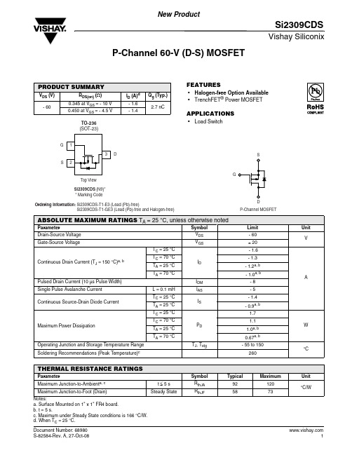
Vishay SiliconixSi2309CDSP-Channel 60-V (D-S) MOSFETFEATURES•Halogen-free Option Available •TrenchFET ® Power MOSFETAPPLICATIONS•Load SwitchPRODUCT SUMMARYV DS (V)R DS(on) (Ω)I D (A)d Q g (Typ.)- 600.345 at V GS = - 10 V - 1.6 2.7 nC0.450 at V GS = - 4.5 V- 1.4Notes:a. Surface Mounted on 1" x 1" FR4 board.b. t = 5 s.c. Maximum under Steady State conditions is 166 °C/W.d. When T C = 25 °C.ABSOLUTE MAXIMUM RATINGS T A = 25 °C, unless otherwise notedParameter Symbol Limit nitDrain-Source Voltage V DS - 60VGate-Source VoltageV GS± 20Continuous Drain Current (T J = 150 °C)a, bT C = 25 °CI D - 1.6A T C = 70 °C - 1.3T A = 25 °C - 1.2a, b T A = 70 °C- 1.0a, bPulsed Drain Current (10 µs Pulse Width)I DM - 8Single Pulse Avalanche Current L = 0.1 mH I AS - 5Continuous Source-Drain Diode CurrentT C = 25 °C I S - 1.4T A = 25 °C - 0.9a, b Maximum Power DissipationT C = 25 °CP D 1.7W T C = 70 °C 1.1T A = 25 °C 1.0a, b T A = 70 °C0.67a, b Operating Junction and Storage T emperature Range T J , T stg - 55 to 150°C Soldering Recommendations (Peak Temperature)c260THERMAL RESISTANCE RATINGSParameter Symbol Typical Maximum UnitMaximum Junction-to-Ambient a, c t ≤ 5 s R thJA 92120°C/WMaximum Junction-to-Foot (Drain)Steady StateR thJF5873Vishay SiliconixSi2309CDSNotes:a. Pulse test; pulse width ≤ 300 µs, duty cycle ≤ 2 %.b. Guaranteed by design, not subject to production testing.Stresses beyond those listed under “Absolute Maximum Ratings” may cause permanent damage to the device. These are stress ratings only, and functional operation of the device at these or any other conditions beyond those indicated in the operational sections of the specifications is not implied. Exposure to absolute maximum rating conditions for extended periods may affect device reliability.SPECIFICATIONS T J = 25 °C, unless otherwise notedParameter Symbol Test Conditions Min.Typ.Max.U nitStaticDrain-Source Breakdown Voltage V DS V GS = 0 V , I D = - 250 µA- 60V V DS Temperature Coefficient ΔV DS /T J I D = - 250 µA - 65mV/°C V GS(th) Temperature Coefficient ΔV GS(th)/T J 4.5Gate-Source Threshold Voltage V GS(th) V DS = V GS , I D = - 250 µA - 1- 3VGate-Source LeakageI GSS V DS = 0 V , V GS = ± 20 V - 100nAZero Gate Voltage Drain Current I DSS V DS = - 60 V , V GS = 0 V - 1µA V DS = - 60 V , V GS = 0 V , T J = 55 °C- 10On-State Drain Current aI D(on) V DS ≤ 5 V , V GS = - 10 V - 6A Drain-Source On-State Resistance a R DS(on) V GS = - 10 V , I D = - 1.25 A 0.2850.345ΩV GS = - 4.5 V , I D = - 1.0 A 0.3600.450Forward T ransconductance a g fsV DS = - 10 V, I D = - 1.0 A2.8SDynamic bInput Capacitance C iss V DS = - 30 V , V GS = 0 V, f = 1 MHz210pFOutput CapacitanceC oss 28Reverse Transfer Capacitance C rss 20Total Gate Charge Q g V DS = - 30 V, V GS = - 4.5 V , ID = - 1.25 A 2.7 4.1nC Gate-Source Charge Q gs 0.8Gate-Drain Charge Q gd 1.2Gate Resistance R g f = 1 MHz7ΩTurn-On Delay Time t d(on) V DD = - 30 V, R L = 30 Ω I D ≅ - 1 A, V GEN = - 4.5 V , R g = 1 Ω4060nsRise Timet r 3555Turn-Off Delay Time t d(off) 1525Fall Timet f 1020Turn-On Delay Time t d(on) V DD = - 30 V, R L = 30 ΩI D ≅ - 1 A, V GEN = - 10 V, R g = 1 Ω510Rise Timet r 1020Turn-Off Delay Time t d(off) 1525Fall Timet f1020Drain-Source Body Diode Characteristics Continuous Source-Drain Diode Current I S T C = 25 °C- 1.4A Pulse Diode Forward Current I SM - 8Body Diode VoltageV SD I S = - 0.75 A, V GS = 0 V- 0.8- 1.2V Body Diode Reverse Recovery Time t rr I F = - 1.25 A, dI/dt = 100 A/µs, T J = 25 °C3060ns Body Diode Reverse Recovery Charge Q rr 3360nC Reverse Recovery Fall Time t a 18nsReverse Recovery Rise Timet b12Gate ChargeOn-Resistance vs. Junction TemperatureSource-Drain Diode Forward VoltageThreshold VoltageSingle Pulse Power, Junction-to-AmbientVishay SiliconixSi2309CDSTYPICAL CHARACTERISTICS 25°C, unless otherwise notedVishay Siliconix maintains worldwide manufacturing capability. Products may be manufactured at one of several qualified locations. Reliability data for Silicon Technology and Package Reliability represent a composite of all qualified locations. For related documents such as package/tape drawings, part marking, and reliability data, see /ppg?68980.Normalized Thermal Transient Impedance, Junction-to-AmbientDisclaimer Legal Disclaimer NoticeVishayAll product specifications and data are subject to change without notice.Vishay Intertechnology, Inc., its affiliates, agents, and employees, and all persons acting on its or their behalf (collectively, “Vishay”), disclaim any and all liability for any errors, inaccuracies or incompleteness contained herein or in any other disclosure relating to any product.Vishay disclaims any and all liability arising out of the use or application of any product described herein or of any information provided herein to the maximum extent permitted by law. The product specifications do not expand or otherwise modify Vishay’s terms and conditions of purchase, including but not limited to the warranty expressed therein, which apply to these products.No license, express or implied, by estoppel or otherwise, to any intellectual property rights is granted by this document or by any conduct of Vishay.The products shown herein are not designed for use in medical, life-saving, or life-sustaining applications unless otherwise expressly indicated. Customers using or selling Vishay products not expressly indicated for use in such applications do so entirely at their own risk and agree to fully indemnify Vishay for any damages arising or resulting from such use or sale. Please contact authorized Vishay personnel to obtain written terms and conditions regarding products designed for such applications.Product names and markings noted herein may be trademarks of their respective owners.元器件交易网。
- 1、下载文档前请自行甄别文档内容的完整性,平台不提供额外的编辑、内容补充、找答案等附加服务。
- 2、"仅部分预览"的文档,不可在线预览部分如存在完整性等问题,可反馈申请退款(可完整预览的文档不适用该条件!)。
- 3、如文档侵犯您的权益,请联系客服反馈,我们会尽快为您处理(人工客服工作时间:9:00-18:30)。
Vishay Siliconix
Si1058X
N-Channel 20-V (D-S) MOSFET
FEATURES
•Halogen-free Option Available •T renchFET ® Power MOSFET •100 % R g and UIS Tested
APPLICATIONS
•Load Switch for Portable Devices
PRODUCT SUMMARY
V DS (V)R DS(on) (Ω)I D (A)Q g (Typ.)20
0.091 at V GS = 4.5 V 1.3a 3.5
0.124 at V GS = 2.5 V
1.1
Notes:
a.Based on T C = 25 °C.
b.Surface Mounted on 1" x 1" FR4 board.
c.t = 5 s.
d.Maximum under Steady State conditions is 650 °C/W.
ABSOLUTE MAXIMUM RATINGS T A = 25 °C, unless otherwise noted
Parameter ymbol Limit Unit Drain-Source Voltage V DS 20
V
Gate-Source Voltage
V GS ± 12Continuous Drain Current (T J = 150 °C)a
T A = 25 °C
I D 1.3b, c
A
T A = 70 °C 1.03b, c
Pulsed Drain Current
I DM 6Avalanche Current L = 0.1 mH
I AS 7
Repetitive Avalanche Energy E AS 2.45mJ
Continuous Source-Drain Diode Current T A = 25 °C I S 0.2b, c
A Maximum Power Dissipation a
T A = 25 °C P D 0.236
b, c W T A = 70 °C 0.151b, c
Operating Junction and Storage T emperature Range T J , T stg - 55 to 150°C
THERMAL RESISTANCE RATINGS
Parameter S
ymbol Typical Maximum Unit
Maximum Junction-to-Ambient b, d
t ≤ 5 s R thJA 440530
°C/W Steady State 540650
Si1058X
Vishay Siliconix
a. Pulse test; pulse width ≤ 300 µs, duty cycle ≤ 2 %.
b. Guaranteed by design, not subject to production testing.
Stresses beyond those listed under “Absolute Maximum Ratings” may cause permanent damage to the device. These are stress ratings only, and functional operation of the device at these or any other conditions beyond those indicated in the operational sections of the specifications is not implied. Exposure to absolute maximum rating conditions for extended periods may affect device reliability.
Vishay Siliconix
Si1058X
TYPICAL CHARACTERISTICS T A = 25 °C, unless otherwise noted
On-Resistance vs. Drain Current
Q g - Gate Charge
On-Resistance vs. Junction Temperature
Vishay Siliconix
Si1058X
TYPICAL CHARACTERISTICS T A = 25 °C, unless otherwise noted
DS(on)GS
Vishay Siliconix
Si1058X
TYPICAL CHARACTERISTICS T A = 25 °C, unless otherwise noted
Vishay Siliconix maintains worldwide manufacturing capability. Products may be manufactured at one of several qualified locations. Reliability data for Silicon
Technology and Package Reliability represent a composite of all qualified locations. For related documents such as package/tape drawings, part marking, and reliability data, see /ppg?73894.
Disclaimer Legal Disclaimer Notice
Vishay
All product specifications and data are subject to change without notice.
Vishay Intertechnology, Inc., its affiliates, agents, and employees, and all persons acting on its or their behalf (collectively, “Vishay”), disclaim any and all liability for any errors, inaccuracies or incompleteness contained herein or in any other disclosure relating to any product.
Vishay disclaims any and all liability arising out of the use or application of any product described herein or of any information provided herein to the maximum extent permitted by law. The product specifications do not expand or otherwise modify Vishay’s terms and conditions of purchase, including but not limited to the warranty expressed therein, which apply to these products.
No license, express or implied, by estoppel or otherwise, to any intellectual property rights is granted by this document or by any conduct of Vishay.
The products shown herein are not designed for use in medical, life-saving, or life-sustaining applications unless otherwise expressly indicated. Customers using or selling Vishay products not expressly indicated for use in such applications do so entirely at their own risk and agree to fully indemnify Vishay for any damages arising or resulting from such use or sale. Please contact authorized Vishay personnel to obtain written terms and conditions regarding products designed for such applications.
Product names and markings noted herein may be trademarks of their respective owners.
元器件交易网。