AT24C32AN-10SU-1.8;AT24C64A-10TU-1.8;AT24C64A-10TU-2.7;中文规格书,Datasheet资料
串行EEPROM AT24CXX芯片资料
串行EEPROM AT24CXX芯片资料AT24CXX是美国ATMEL公司的低功耗CMOS串行EEPROM,典型的型号有AT24C01A/02/04/08/16等5种,它们的存储容量分别是1024/2048/4096/8192/16384位;也就是128/256/512/1024/2048字节;使用电压级别有5V,2.7V,2.5V,1.8V;本文主要介绍常用的AT24C02即256字节存储器的使用;它具有工作电压宽(2.5~5.5V)、擦写次数多(大于10000次)、写入速度快(小于10ms)等特点。
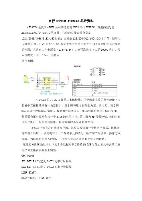
外行如图:AT24C02的1、2、3脚是三条地址线,用于确定芯片的硬件地址(实验板中直接接地只有一块器件);第8脚和第4脚分别为正、负电源。
第5脚SDA为串行数据输入/输出,数据通过这条双向I2C总线串行传送,SDA和SCL都需要和正电源间各接一个5.1K的电阻上拉。
第7脚为WP写保护端,接地时允许芯片执行一般的读写操作。
接电源端时不允许对器件写。
24C02中带有片内地址寄存器。
每写入或读出一个数据字节后,该地址寄存器自动加1,以实现对下一个存储单元的读写。
所有字节均以单一操作方式读取。
为降低总的写入时间,一次操作可写入多达8个字节的数据。
;这是将0100H地址中以下的8个数据写到24C02的01H为首址单元中去的汇编程序可直接在实验板上实验。
ORG 0000HSCL BIT P3.7;定义24C02的串行时钟线SDA BIT P3.6;定义24C02的串行数据线LJMP STARTSTART:LCALL STAR;调用MOV R2,#08H;一个数据有8位MOV DPTR,#0100H;定义源数据的位置LOOP:MOV A,#00HMOVC A,@A+DPTRLCALL SDATALCALL ACKJC LOOPINC DPTRDJNZ R2,LOOPLCALL STOP;调用停止子程序STAR:SETB SDASETB SCLNOPNOPNOPNOPCLR SDANOPNOPNOPNOPCLR SCLRETSDATA:MOV R0,#08HLOOP0:RLC AMOV SDA,CNOPNOPSETB SCLNOPNOPNOPCLR SCLDJNZ R0,LOOP0 RETACK:SETB SDA NOPNOPSETB SCL NOPNOPNOPNOPMOV C,SDA CLR SCLRETSTOP:CLR SDA NOPNOPNOPNOPSETB SCL NOPNOPNOPNOPSETB SDANOPNOPNOPRETORG 0100HDB 0A0H,10H,01H,02H,03H,04H,05H,06HEND读写子程序如下:;写串行E2PROM子程序XEPR; R3=10100000(命令1010+器件3位地址+读/写。
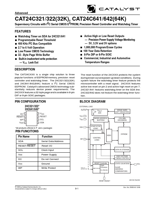
CAT24C323中文资料
© 1998 by Catalyst Semiconductor, Inc. Characteristics subject to change without noticeDoc. No. 25083-00 12/989-1CAT24C321/322/641/6422AdvancedDoc. No. 25083-00 12/98ABSOLUTE MAXIMUM RATINGS*Temperature Under Bias....................–55°C to +125°C Storage Temperature........................ –65°C to +150°C Voltage on Any Pin withRespect to Ground (1) ..............–2.0V to +V CC + 2.0V V CC with Respect to Ground..................–2.0V to +7.0V Package Power DissipationCapability (Ta = 25°C)1.0W.................................1.0W Lead Soldering Temperature (10 secs)...............300°C Output Short Circuit Current (2) ..........................100mACOMMENTStresses above those listed under “Absolute Maximum Ratings” may cause permanent damage to the device.These are stress ratings only, and functional operation of the device at these or any other conditions outside of those listed in the operational sections of this specifica-tion is not implied. Exposure to any absolute maximum rating for extended periods may affect device perfor-mance and reliability.RELIABILITY CHARACTERISTICSSymbol Parameter Min.Max. Units Reference Test MethodN END (3)Endurance 1,000,000 Cycles/Byte MIL-STD-883, Test Method 1033 T DR (3)Data Retention 100 Years MIL-STD-883, Test Method 1008 V ZAP (3)ESD Susceptibility 2000 Volts MIL-STD-883, Test Method 3015 I LTH (3)(4)Latch-up 100 mAJEDEC Standard 17D.C. OPERATING CHARACTERISTICSV CC = +2.7V to +6.0V, unless otherwise specified.Symbol Parameter Min. Typ. Max. Units Test Conditions I CC Power Supply Current 3mA f SCL = 100 KHzIsbStandby Current40 µAVcc=3.3V50 µA Vcc=5I LI Input Leakage Current 2 µA V IN =G ND or V CC I LO Output Leakage Current10µA V IN =G ND or V CCV IL Input Low Voltage –1 V CC x 0.3 V V IH Input High Voltage V CC x 0.7 V CC + 0.5 VV OLOutput Low Voltage (SDA)0.4 V I OL = 3 mA ,V CC =3.0VLimitsCAPACITANCE T A = 25°C, f = 1.0 MHz, V CC = 5V Symbol Test Max.Units Conditions C I/O (3) Input/Output Capacitance (SDA)8pF V I/O = 0V C IN (3)Input Capacitance (SCL)6pFV IN = 0VNote:(1)The minimum DC input voltage is –0.5V. During transitions, inputs may undershoot to –2.0V for periods of less than 20 ns. Maximum DCvoltage on output pins is V CC +0.5V, which may overshoot to V CC + 2.0V for periods of less than 20ns.(2)Output shorted for no more than one second. No more than one output shorted at a time.(3)This parameter is tested initially and after a design or process change that affects the parameter.(4)Latch-up protection is provided for stresses up to 100 mA on address and data pins from –1V to V CC +1V.CAT24C321/322/641/6423AdvancedDoc. No. 25083-00 12/98A.C. CHARACTERISTICSV CC =2.7V to 6.0V unless otherwise specified.Output Load is 1 TTL Gate and 100pFRead & Write Cycle Limits SymbolParameterV CC =2.7V - 6V V CC =4.5V - 5.5V Min.Max.Min.Max.Units F SCL Clock Frequency100400kHz T I (1)Noise Suppression Time200200ns Constant at SCL, SDA Inputs t AA SCL Low to SDA Data Out 3.51µs and ACK Outt BUF (1)Time the Bus Must be Free Before 4.7 1.2µs a New Transmission Can Start t HD:STA Start Condition Hold Time 40.6µs t LOW Clock Low Period 4.7 1.2µs t HIGH Clock High Period40.6µs t SU:STA Start Condition Setup Time4.70.6µs (for a Repeated Start Condition)t HD:DAT Data In Hold Time 00ns t SU:DAT Data In Setup Time 5050ns t R (1)SDA and SCL Rise Time 10.3µs t F (1)SDA and SCL Fall Time 300300ns t SU:STO Stop Condition Setup Time 40.6µs t DHData Out Hold Time100100nsPower-Up Timing (1)(2)Symbol ParameterMax.Units t PUR Power-up to Read Operation 1ms t PUWPower-up to Write Operation1msNote:(1)This parameter is tested initially and after a design or process change that affects the parameter.(2)t PUR and t PUW are the delays required from the time V CC is stable until the specified operation can be initiated.Write Cycle Limits Symbol Parameter Min.Typ.Max Units t WRWrite Cycle Time10msThe write cycle time is the time from a valid stop condition of a write sequence to the end of the internal program/erase cycle. During the write cycle, the bus interface circuits are disabled, SDA is allowed to remain high, and the device does not respond to its slave address.CAT24C321/322/641/6424AdvancedDoc. No. 25083-00 12/98RESET CIRCUIT CHARACTERISTICSCAT24C321/322/641/6425AdvancedDoc. No. 25083-00 12/98PIN DESCRIPTIONSWP : WRITE PROTECTIf the pin is tied to V CC the entire memory array becomes Write Protected (READ only). When the pin is tied to V SS or left floating normal read/write operations are allowed to the device.SCL : SERIAL CLOCKThe serial clock input clocks all data transferred into or out of the device.RESET/RESET : RESET I/OThese are open drain pins and can be used as reset trigger inputs. By forcing a reset condition on the pins the device will initiate and maintain a reset condition for approximately 200ms. RESET pin must be connected through a pull-down and RESET pin must be connected through a pull-up device.SDA: SERIAL DATA/ADDRESSThe bidirectional serial data/address pin is used to transfer all data into and out of the device. The SDA pin is an open drain output and can be wire-ORed with other open drain or open collector outputs. In the 24C321/641, the SDA line is also used as the Watchdog Timer Monitor.Reset Controller DescriptionThe CAT24CXXX provides a precision RESET control-ler that ensures correct system operation during brown-out and power-up/down conditions. It is configured with open drain RESET outputs. During power-up, the RESET outputs remain active until V CC reaches the V TH threshold and will continue driving the outputs for approximately 200ms (t PURST ) after reaching V TH. After the t PURST timeout interval, the device will cease to drive reset outputs. At this point the reset outputs will be pulled up or down by their respective pull up/pull down devices. During power-down, the RESET outputs will begin driving active when V CC falls below V TH. The RESET outputs will be valid so long as V CC is >1.0V (V RVALID ).The RESET pins are I/Os; therefore, the CAT24CXXX can act as a signal conditioning circuit for an externally applied reset. The inputs are level triggered; that is, the RESET input in the 24CXXX will initiate a reset timeout after detecting a high and the RESET input in the 24CXXX will initiate a reset timeout after detecting a low.Watchdog TimerThe Watchdog Timer provides an independent protec-tion for microcontrollers. During a system failure, the CAT24C321/641 will respond with a reset signal after a time-out interval of 1.6 seconds for lack of activity.24CXX1 is designed with the Watchdog Timer feature on the SDA input. For the 24C321/641, if the microcontroller does not toggle the SDA input pin within 1.6 seconds the Watchdog Timer times out. This will generate a reset condition on reset outputs. The Watch-dog Timer is cleared by any transition on SDA.As long as the reset signal is asserted, the Watchdog Timer will not count and will stay cleared. 24C322/642does not feature the Watchdog Timer function.DEVICE OPERATIONV CCV RESETCAT24C321/322/641/6426AdvancedDoc. No. 25083-00 12/98Hardware Data ProtectionThe 24CXXX is designed with the following hardware data protection features to provide a high degree of data integrity.(1) The 24CXXX features a WP pin. When WP pin is tied high the entire memory array becomes write protected (read only).(2) The V CC sense provides write protection when V CC falls below the reset threshold value (V TH ). The V CC lock out inhibits writes to the serial EEPROM whenever V CC falls below (power down) V TH or until V CC reaches the reset threshold (power up) V TH .Reset Threshold VoltageFrom the factory the 24CXXX is offered in five different variations of reset threshold voltages. They are 4.50-4.75V, 4.25-4.50V, 3.00-3.15V, 2.85-3.00V and 2.55-2.70V. To provide added flexibility to design engineers using this product, the 24CXXX is designed with an additional feature of programming the reset threshold voltage. This allows the user to change the existing reset threshold voltage to one of the other four reset threshold voltages. Once the reset threshold voltage is selected it will not change even after cycling the power,unless the user uses the programmer to change the reset threshold voltage. However, the programming function is available only through third party programmer manufacturers. Please call Catalyst for a list of program-mer manufacturers who support this function.STOPCONDITIONSTARTCONDITIONADDRESSSCLSDAFigure 3. Write Cycle TimingSTART BITSDASTOP BITSCLFigure 4. Start/Stop TimingSCLSDA INSDA OUTFigure 2. Bus TimingCAT24C321/322/641/6427AdvancedDoc. No. 25083-00 12/98ACKNOWLEDGESTARTSCL FROM MASTERDATA OUTPUTFROM TRANSMITTERDATA OUTPUT FROM RECEIVERFigure 5. Acknowledge TimingFigure 6. Slave Address BitsFUNCTIONAL DESCRIPTIONThe CAT24CXXX supports the I 2C Bus data transmis-sion protocol. This Inter-Integrated Circuit Bus protocol defines any device that sends data to the bus to be a transmitter and any device receiving data to be a re-ceiver. The transfer is controlled by the Master device which generates the serial clock and all START and STOP conditions for bus access. The CAT24CXXX operates as a Slave device. Both the Master device and Slave device can operate as either transmitter or re-ceiver, but the Master device controls which mode is activated.I 2C BUS PROTOCOLThe features of the I 2C bus protocol are defined as follows:(1) Data transfer may be initiated only when the bus is not busy.(2) During a data transfer, the data line must remain stable whenever the clock line is high. Any changes in the data line while the clock line is high will be interpreted as a START or STOP condition.START ConditionThe START Condition precedes all commands to the device, and is defined as a HIGH to LOW transition of SDA when SCL is HIGH. The CAT24CXXX monitors the SDA and SCL lines and will not respond until this condition is met.STOP ConditionA LOW to HIGH transition of SDA when SCL is HIGH determines the STOP condition. All operations must end with a STOP condition.DEVICE ADDRESSINGThe Master begins a transmission by sending a START condition. The Master sends the address of the particu-lar slave device it is requesting. The four most significant bits of the 8-bit slave address are fixed as 1010.The next three bits are don't care. The last bit of the slave address specifies whether a Read or Write operation is to be performed. When this bit is set to 1, a Read operation is selected, and when set to 0, a Write opera-tion is selected.After the Master sends a START condition and the slave address byte, the CAT24CXXX monitors the bus and responds with an acknowledge (on the SDA line) when its address matches the transmitted slave address. The CAT24CXXX then performs a Read or Write operation depending on the state of the R/W bit.1010X R/WX XCAT24C321/322/641/6428AdvancedDoc. No. 25083-00 12/98Figure 7. Byte Write TimingFigure 8. Page Write TimingACKNOWLEDGEAfter a successful data transfer, each receiving device is required to generate an acknowledge. The Acknowledg-ing device pulls down the SDA line during the ninth clock cycle, signaling that it received the 8 bits of data.The CAT24CXXX responds with an acknowledge after receiving a START condition and its slave address. If the device has been selected along with a write operation,it responds with an acknowledge after receiving each 8-bit byte.When the CAT24CXXX begins a READ mode it trans-mits 8 bits of data, releases the SDA line, and monitors the line for an acknowledge. Once it receives this ac-knowledge, the CAT24CXXX will continue to transmit data. If no acknowledge is sent by the Master, the device terminates data transmission and waits for a STOP condition.WRITE OPERATIONSByte WriteIn the Byte Write mode, the Master device sends the START condition and the slave address information (with the R/W bit set to zero) to the Slave device. After t he Slave generates an acknowledge, the Master sends a 8-bit address that is to be written into the address pointers of the CAT24CXXX. After receiving another acknowledge from the Slave, the Master device trans-mits the data to be written into the addressed memory location. The CAT24CXXX acknowledges once more and the Master generates the STOP condition. At this time, the device begins an internal programming cycle to nonvolatile memory. While the cycle is in progress, the device will not respond to any request from the Master device.Page WriteThe 24CXXX writes up to 32 bytes of data in a single write cycle, using the Page Write operation. The page write operation is initiated in the same manner as the byte write operation, however instead of terminating after the initial byte is transmitted, the Master is allowed to send up to 31 additional bytes. After each byte has been transmitted, CAT24CXXX will respond with an acknowledge, and internally increment the lower order address bits by one. The high order bits remain un-changed.If the Master transmits more than 32 bytes before sending the STOP condition, the address counter ‘wraps around’, and previously transmitted data will be overwrit-ten.When all 32 bytes are received, and the STOP condi tion has been sent by the Master, the internal program-ming cycle begins. At this point, all received data is written to the CAT24CXXX in a single write cycle.* = Don't care bit for 24C321/322X= Don't care bitA 15–A 8SLAVE ADDRESSSA C KAC KDATAA C KS T O P P BUS ACTIVITY:MASTERSDA LINES T A R T A 7–A 0BYTE ADDRESS A C K*X X XSLAVE C KC KC KBUS ACTIVITY:MASTERSDA LINES T A BYTE ADDRESS C KS T C K C KC KCAT24C321/322/641/6429AdvancedDoc. No. 25083-00 12/98Figure 9. Immediate Address Read TimingAcknowledge PollingDisabling of the inputs can be used to take advantage of the typical write cycle time. Once the stop condition is issued to indicate the end of the host’s write operation,CAT24CXXX initiates the internal write cycle. ACK poll-ing can be initiated immediately. This involves issuing the start condition followed by the slave address for a write operation. If CAT24CXXX is still busy with the write operation, no ACK will be returned. If CAT24CXXX has completed the write operation, an ACK will be returned and the host can then proceed with the next read or write operation.WRITE PROTECTIONThe Write Protection feature allows the user to protect against inadvertent programming of the memory array.If the WP pin is tied to V CC , the entire memory array is protected and becomes read only. The CAT24CXXX will accept both slave and byte addresses, but the memory location accessed is protected from program-ming by the device's failure to send an acknowledge after the first byte of data is received.READ OPERATIONSThe READ operation for the CAT24CXXX is initiated in the same manner as the write operation with one excep-tion, that R/W bit is set to one. Three different READ operations are possible: Immediate/Current Address READ, Selective/Random READ and Sequential READ.SCL SDA 8TH BIT STOPNO ACKDATA OUT89SLAVE ADDRESSSA C KBUS ACTIVITY:MASTERSDA LINES T A R T N O A C KDATAS T O P PCAT24C321/322/641/64210AdvancedDoc. No. 25083-00 12/98Figure 10. Selective Read TimingFigure 11. Sequential Read TimingImmediate/Current Address ReadThe CAT24CXXX’s address counter contains the ad-dress of the last byte accessed, incremented by one. In other words, if the last READ or WRITE access was to address N, the READ immediately following would ac-cess data from address N+1. If N=E (where E=4095 for 24C321/322 and E=8191 for 24C641/642), then the counter will ‘wrap around’ to address 0 and continue to clock out data. After the CAT24CXXX receives its slave address information (with the R/W bit set to one), it issues an acknowledge, then transmits the 8-bit byte requested. The master device does not send an ac-knowledge, but will generate a STOP condition.Selective/Random ReadSelective/Random READ operations allow the Master device to select at random any memory location for a READ operation. The Master device first performs a ‘dummy’ write operation by sending the START condi-tion, slave address and byte addresses of the location it wishes to read. After CAT24CXXX acknowledges, the Master device sends the START condition and the slave address again, this time with the R/W bit set to one.The CAT24CXXX then responds with its acknowledge and sends the 8-bit byte requested. The master deviceSequential ReadThe Sequential READ operation can be initiated by either the Immediate Address READ or Selective READ operations. After the CAT24CXXX sends the initial 8-bit byte requested, the Master will respond with an acknowledge which tells the device it requires more data. The CAT24CXXX will continue to output an 8-bit byte for each acknowledge sent by the Master. The operation will terminate when the Master fails to respond with an acknowledge, thus sending the STOP condition.The data being transmitted from CAT24CXXX is output-ted sequentially with data from address N followed by data from address N+1. The READ operation address counter increments all of the CAT24CXXX address bits so that the entire memory array can be read during one operation. If more than E (where E= 4095 for 24C321/322, E=511 and E=8191 for 24C641/642) bytes are read out, the counter will ‘wrap around’ and continue to clock out data bytes.does not send an acknowledge but will generate a STOP condition.BUS ACTIVITY:MASTERSDA LINEDATA n+xDATA nC KC KDATA n+1C KS T O O A C KDATA n+2C KSLAVE ADDRESS* = Don't care bit for 24C321/322X= Don't care bitA 15–A 8SLAVE ADDRESSSA C KA C KA C KBUS ACTIVITY:MASTERSDA LINES T A R T A 7–A 0BYTE ADDRESS SLAVEADDRESSSA C KN O A C KS T A R T DATAPS T O P X X X *CAT24C321/322/641/64211Advanced Doc. No. 25083-00 12/98Ordering InformationNote:(1) The device used in the above example is a CAT24C322JI-30TE13 (32K I 2C Memory, SOIC, Industrial Temperature, 3.0-3.15V ResetThreshold Voltage, Tape and Reel)CAT24C321/322/641/64212AdvancedDoc. No. 25083-00 12/98。
M24C32,M24C64--存储芯片手册免费下载

64Kbit and 32Kbit Serial I²C Bus EEPROM
FEATURES SUMMARY
■ Two-Wire I2C Serial Interface Supports 400kHz Protocol
■ Single Supply Voltage: – 4.5 to 5.5V for M24Cxx – 2.5 to 5.5V for M24Cxx-W – 1.8 to 5.5V for M24Cxx-R
Table 1. Product List
Reference
Part Number
M24C64
M24C64
M24C64-W
M24C64-R
M24C32
M24C32
M24C32-W
M24C32-R
Figure 1. Packages
8 1
PDIP8 (BN)
8 1
SO8 (MN) 150 mil width
MEMORY ORGANIZATION . . . . . . . . . . . . . . . . . . . . . . . . . . . . . . . . . . . . . . . . . . . . . . . . . . . . . . . . . . 7 Figure 6. Block Diagram . . . . . . . . . . . . . . . . . . . . . . . . . . . . . . . . . . . . . . . . . . . . . . . . . . . . . . . . . . 7
TSSOP8 (DW) 169 mil width
UFDFPN8 (MB) 2x3mm² (MLP)
CAT24C321中文资料
© 1998 by Catalyst Semiconductor, Inc. Characteristics subject to change without noticeDoc. No. 25083-00 12/989-1CAT24C321/322/641/6422AdvancedDoc. No. 25083-00 12/98ABSOLUTE MAXIMUM RATINGS*Temperature Under Bias....................–55°C to +125°C Storage Temperature........................ –65°C to +150°C Voltage on Any Pin withRespect to Ground (1) ..............–2.0V to +V CC + 2.0V V CC with Respect to Ground..................–2.0V to +7.0V Package Power DissipationCapability (Ta = 25°C)1.0W.................................1.0W Lead Soldering Temperature (10 secs)...............300°C Output Short Circuit Current (2) ..........................100mACOMMENTStresses above those listed under “Absolute Maximum Ratings” may cause permanent damage to the device.These are stress ratings only, and functional operation of the device at these or any other conditions outside of those listed in the operational sections of this specifica-tion is not implied. Exposure to any absolute maximum rating for extended periods may affect device perfor-mance and reliability.RELIABILITY CHARACTERISTICSSymbol Parameter Min.Max. Units Reference Test MethodN END (3)Endurance 1,000,000 Cycles/Byte MIL-STD-883, Test Method 1033 T DR (3)Data Retention 100 Years MIL-STD-883, Test Method 1008 V ZAP (3)ESD Susceptibility 2000 Volts MIL-STD-883, Test Method 3015 I LTH (3)(4)Latch-up 100 mAJEDEC Standard 17D.C. OPERATING CHARACTERISTICSV CC = +2.7V to +6.0V, unless otherwise specified.Symbol Parameter Min. Typ. Max. Units Test Conditions I CC Power Supply Current 3mA f SCL = 100 KHzIsbStandby Current40 µAVcc=3.3V50 µA Vcc=5I LI Input Leakage Current 2 µA V IN =G ND or V CC I LO Output Leakage Current10µA V IN =G ND or V CCV IL Input Low Voltage –1 V CC x 0.3 V V IH Input High Voltage V CC x 0.7 V CC + 0.5 VV OLOutput Low Voltage (SDA)0.4 V I OL = 3 mA ,V CC =3.0VLimitsCAPACITANCE T A = 25°C, f = 1.0 MHz, V CC = 5V Symbol Test Max.Units Conditions C I/O (3) Input/Output Capacitance (SDA)8pF V I/O = 0V C IN (3)Input Capacitance (SCL)6pFV IN = 0VNote:(1)The minimum DC input voltage is –0.5V. During transitions, inputs may undershoot to –2.0V for periods of less than 20 ns. Maximum DCvoltage on output pins is V CC +0.5V, which may overshoot to V CC + 2.0V for periods of less than 20ns.(2)Output shorted for no more than one second. No more than one output shorted at a time.(3)This parameter is tested initially and after a design or process change that affects the parameter.(4)Latch-up protection is provided for stresses up to 100 mA on address and data pins from –1V to V CC +1V.CAT24C321/322/641/6423AdvancedDoc. No. 25083-00 12/98A.C. CHARACTERISTICSV CC =2.7V to 6.0V unless otherwise specified.Output Load is 1 TTL Gate and 100pFRead & Write Cycle Limits SymbolParameterV CC =2.7V - 6V V CC =4.5V - 5.5V Min.Max.Min.Max.Units F SCL Clock Frequency100400kHz T I (1)Noise Suppression Time200200ns Constant at SCL, SDA Inputs t AA SCL Low to SDA Data Out 3.51µs and ACK Outt BUF (1)Time the Bus Must be Free Before 4.7 1.2µs a New Transmission Can Start t HD:STA Start Condition Hold Time 40.6µs t LOW Clock Low Period 4.7 1.2µs t HIGH Clock High Period40.6µs t SU:STA Start Condition Setup Time4.70.6µs (for a Repeated Start Condition)t HD:DAT Data In Hold Time 00ns t SU:DAT Data In Setup Time 5050ns t R (1)SDA and SCL Rise Time 10.3µs t F (1)SDA and SCL Fall Time 300300ns t SU:STO Stop Condition Setup Time 40.6µs t DHData Out Hold Time100100nsPower-Up Timing (1)(2)Symbol ParameterMax.Units t PUR Power-up to Read Operation 1ms t PUWPower-up to Write Operation1msNote:(1)This parameter is tested initially and after a design or process change that affects the parameter.(2)t PUR and t PUW are the delays required from the time V CC is stable until the specified operation can be initiated.Write Cycle Limits Symbol Parameter Min.Typ.Max Units t WRWrite Cycle Time10msThe write cycle time is the time from a valid stop condition of a write sequence to the end of the internal program/erase cycle. During the write cycle, the bus interface circuits are disabled, SDA is allowed to remain high, and the device does not respond to its slave address.CAT24C321/322/641/6424AdvancedDoc. No. 25083-00 12/98RESET CIRCUIT CHARACTERISTICSCAT24C321/322/641/6425AdvancedDoc. No. 25083-00 12/98PIN DESCRIPTIONSWP : WRITE PROTECTIf the pin is tied to V CC the entire memory array becomes Write Protected (READ only). When the pin is tied to V SS or left floating normal read/write operations are allowed to the device.SCL : SERIAL CLOCKThe serial clock input clocks all data transferred into or out of the device.RESET/RESET : RESET I/OThese are open drain pins and can be used as reset trigger inputs. By forcing a reset condition on the pins the device will initiate and maintain a reset condition for approximately 200ms. RESET pin must be connected through a pull-down and RESET pin must be connected through a pull-up device.SDA: SERIAL DATA/ADDRESSThe bidirectional serial data/address pin is used to transfer all data into and out of the device. The SDA pin is an open drain output and can be wire-ORed with other open drain or open collector outputs. In the 24C321/641, the SDA line is also used as the Watchdog Timer Monitor.Reset Controller DescriptionThe CAT24CXXX provides a precision RESET control-ler that ensures correct system operation during brown-out and power-up/down conditions. It is configured with open drain RESET outputs. During power-up, the RESET outputs remain active until V CC reaches the V TH threshold and will continue driving the outputs for approximately 200ms (t PURST ) after reaching V TH. After the t PURST timeout interval, the device will cease to drive reset outputs. At this point the reset outputs will be pulled up or down by their respective pull up/pull down devices. During power-down, the RESET outputs will begin driving active when V CC falls below V TH. The RESET outputs will be valid so long as V CC is >1.0V (V RVALID ).The RESET pins are I/Os; therefore, the CAT24CXXX can act as a signal conditioning circuit for an externally applied reset. The inputs are level triggered; that is, the RESET input in the 24CXXX will initiate a reset timeout after detecting a high and the RESET input in the 24CXXX will initiate a reset timeout after detecting a low.Watchdog TimerThe Watchdog Timer provides an independent protec-tion for microcontrollers. During a system failure, the CAT24C321/641 will respond with a reset signal after a time-out interval of 1.6 seconds for lack of activity.24CXX1 is designed with the Watchdog Timer feature on the SDA input. For the 24C321/641, if the microcontroller does not toggle the SDA input pin within 1.6 seconds the Watchdog Timer times out. This will generate a reset condition on reset outputs. The Watch-dog Timer is cleared by any transition on SDA.As long as the reset signal is asserted, the Watchdog Timer will not count and will stay cleared. 24C322/642does not feature the Watchdog Timer function.DEVICE OPERATIONV CCV RESETCAT24C321/322/641/6426AdvancedDoc. No. 25083-00 12/98Hardware Data ProtectionThe 24CXXX is designed with the following hardware data protection features to provide a high degree of data integrity.(1) The 24CXXX features a WP pin. When WP pin is tied high the entire memory array becomes write protected (read only).(2) The V CC sense provides write protection when V CC falls below the reset threshold value (V TH ). The V CC lock out inhibits writes to the serial EEPROM whenever V CC falls below (power down) V TH or until V CC reaches the reset threshold (power up) V TH .Reset Threshold VoltageFrom the factory the 24CXXX is offered in five different variations of reset threshold voltages. They are 4.50-4.75V, 4.25-4.50V, 3.00-3.15V, 2.85-3.00V and 2.55-2.70V. To provide added flexibility to design engineers using this product, the 24CXXX is designed with an additional feature of programming the reset threshold voltage. This allows the user to change the existing reset threshold voltage to one of the other four reset threshold voltages. Once the reset threshold voltage is selected it will not change even after cycling the power,unless the user uses the programmer to change the reset threshold voltage. However, the programming function is available only through third party programmer manufacturers. Please call Catalyst for a list of program-mer manufacturers who support this function.STOPCONDITIONSTARTCONDITIONADDRESSSCLSDAFigure 3. Write Cycle TimingSTART BITSDASTOP BITSCLFigure 4. Start/Stop TimingSCLSDA INSDA OUTFigure 2. Bus TimingCAT24C321/322/641/6427AdvancedDoc. No. 25083-00 12/98ACKNOWLEDGESTARTSCL FROM MASTERDATA OUTPUTFROM TRANSMITTERDATA OUTPUT FROM RECEIVERFigure 5. Acknowledge TimingFigure 6. Slave Address BitsFUNCTIONAL DESCRIPTIONThe CAT24CXXX supports the I 2C Bus data transmis-sion protocol. This Inter-Integrated Circuit Bus protocol defines any device that sends data to the bus to be a transmitter and any device receiving data to be a re-ceiver. The transfer is controlled by the Master device which generates the serial clock and all START and STOP conditions for bus access. The CAT24CXXX operates as a Slave device. Both the Master device and Slave device can operate as either transmitter or re-ceiver, but the Master device controls which mode is activated.I 2C BUS PROTOCOLThe features of the I 2C bus protocol are defined as follows:(1) Data transfer may be initiated only when the bus is not busy.(2) During a data transfer, the data line must remain stable whenever the clock line is high. Any changes in the data line while the clock line is high will be interpreted as a START or STOP condition.START ConditionThe START Condition precedes all commands to the device, and is defined as a HIGH to LOW transition of SDA when SCL is HIGH. The CAT24CXXX monitors the SDA and SCL lines and will not respond until this condition is met.STOP ConditionA LOW to HIGH transition of SDA when SCL is HIGH determines the STOP condition. All operations must end with a STOP condition.DEVICE ADDRESSINGThe Master begins a transmission by sending a START condition. The Master sends the address of the particu-lar slave device it is requesting. The four most significant bits of the 8-bit slave address are fixed as 1010.The next three bits are don't care. The last bit of the slave address specifies whether a Read or Write operation is to be performed. When this bit is set to 1, a Read operation is selected, and when set to 0, a Write opera-tion is selected.After the Master sends a START condition and the slave address byte, the CAT24CXXX monitors the bus and responds with an acknowledge (on the SDA line) when its address matches the transmitted slave address. The CAT24CXXX then performs a Read or Write operation depending on the state of the R/W bit.1010X R/WX XCAT24C321/322/641/6428AdvancedDoc. No. 25083-00 12/98Figure 7. Byte Write TimingFigure 8. Page Write TimingACKNOWLEDGEAfter a successful data transfer, each receiving device is required to generate an acknowledge. The Acknowledg-ing device pulls down the SDA line during the ninth clock cycle, signaling that it received the 8 bits of data.The CAT24CXXX responds with an acknowledge after receiving a START condition and its slave address. If the device has been selected along with a write operation,it responds with an acknowledge after receiving each 8-bit byte.When the CAT24CXXX begins a READ mode it trans-mits 8 bits of data, releases the SDA line, and monitors the line for an acknowledge. Once it receives this ac-knowledge, the CAT24CXXX will continue to transmit data. If no acknowledge is sent by the Master, the device terminates data transmission and waits for a STOP condition.WRITE OPERATIONSByte WriteIn the Byte Write mode, the Master device sends the START condition and the slave address information (with the R/W bit set to zero) to the Slave device. After t he Slave generates an acknowledge, the Master sends a 8-bit address that is to be written into the address pointers of the CAT24CXXX. After receiving another acknowledge from the Slave, the Master device trans-mits the data to be written into the addressed memory location. The CAT24CXXX acknowledges once more and the Master generates the STOP condition. At this time, the device begins an internal programming cycle to nonvolatile memory. While the cycle is in progress, the device will not respond to any request from the Master device.Page WriteThe 24CXXX writes up to 32 bytes of data in a single write cycle, using the Page Write operation. The page write operation is initiated in the same manner as the byte write operation, however instead of terminating after the initial byte is transmitted, the Master is allowed to send up to 31 additional bytes. After each byte has been transmitted, CAT24CXXX will respond with an acknowledge, and internally increment the lower order address bits by one. The high order bits remain un-changed.If the Master transmits more than 32 bytes before sending the STOP condition, the address counter ‘wraps around’, and previously transmitted data will be overwrit-ten.When all 32 bytes are received, and the STOP condi tion has been sent by the Master, the internal program-ming cycle begins. At this point, all received data is written to the CAT24CXXX in a single write cycle.* = Don't care bit for 24C321/322X= Don't care bitA 15–A 8SLAVE ADDRESSSA C KAC KDATAA C KS T O P P BUS ACTIVITY:MASTERSDA LINES T A R T A 7–A 0BYTE ADDRESS A C K*X X XSLAVE C KC KC KBUS ACTIVITY:MASTERSDA LINES T A BYTE ADDRESS C KS T C K C KC KCAT24C321/322/641/6429AdvancedDoc. No. 25083-00 12/98Figure 9. Immediate Address Read TimingAcknowledge PollingDisabling of the inputs can be used to take advantage of the typical write cycle time. Once the stop condition is issued to indicate the end of the host’s write operation,CAT24CXXX initiates the internal write cycle. ACK poll-ing can be initiated immediately. This involves issuing the start condition followed by the slave address for a write operation. If CAT24CXXX is still busy with the write operation, no ACK will be returned. If CAT24CXXX has completed the write operation, an ACK will be returned and the host can then proceed with the next read or write operation.WRITE PROTECTIONThe Write Protection feature allows the user to protect against inadvertent programming of the memory array.If the WP pin is tied to V CC , the entire memory array is protected and becomes read only. The CAT24CXXX will accept both slave and byte addresses, but the memory location accessed is protected from program-ming by the device's failure to send an acknowledge after the first byte of data is received.READ OPERATIONSThe READ operation for the CAT24CXXX is initiated in the same manner as the write operation with one excep-tion, that R/W bit is set to one. Three different READ operations are possible: Immediate/Current Address READ, Selective/Random READ and Sequential READ.SCL SDA 8TH BIT STOPNO ACKDATA OUT89SLAVE ADDRESSSA C KBUS ACTIVITY:MASTERSDA LINES T A R T N O A C KDATAS T O P PCAT24C321/322/641/64210AdvancedDoc. No. 25083-00 12/98Figure 10. Selective Read TimingFigure 11. Sequential Read TimingImmediate/Current Address ReadThe CAT24CXXX’s address counter contains the ad-dress of the last byte accessed, incremented by one. In other words, if the last READ or WRITE access was to address N, the READ immediately following would ac-cess data from address N+1. If N=E (where E=4095 for 24C321/322 and E=8191 for 24C641/642), then the counter will ‘wrap around’ to address 0 and continue to clock out data. After the CAT24CXXX receives its slave address information (with the R/W bit set to one), it issues an acknowledge, then transmits the 8-bit byte requested. The master device does not send an ac-knowledge, but will generate a STOP condition.Selective/Random ReadSelective/Random READ operations allow the Master device to select at random any memory location for a READ operation. The Master device first performs a ‘dummy’ write operation by sending the START condi-tion, slave address and byte addresses of the location it wishes to read. After CAT24CXXX acknowledges, the Master device sends the START condition and the slave address again, this time with the R/W bit set to one.The CAT24CXXX then responds with its acknowledge and sends the 8-bit byte requested. The master deviceSequential ReadThe Sequential READ operation can be initiated by either the Immediate Address READ or Selective READ operations. After the CAT24CXXX sends the initial 8-bit byte requested, the Master will respond with an acknowledge which tells the device it requires more data. The CAT24CXXX will continue to output an 8-bit byte for each acknowledge sent by the Master. The operation will terminate when the Master fails to respond with an acknowledge, thus sending the STOP condition.The data being transmitted from CAT24CXXX is output-ted sequentially with data from address N followed by data from address N+1. The READ operation address counter increments all of the CAT24CXXX address bits so that the entire memory array can be read during one operation. If more than E (where E= 4095 for 24C321/322, E=511 and E=8191 for 24C641/642) bytes are read out, the counter will ‘wrap around’ and continue to clock out data bytes.does not send an acknowledge but will generate a STOP condition.BUS ACTIVITY:MASTERSDA LINEDATA n+xDATA nC KC KDATA n+1C KS T O O A C KDATA n+2C KSLAVE ADDRESS* = Don't care bit for 24C321/322X= Don't care bitA 15–A 8SLAVE ADDRESSSA C KA C KA C KBUS ACTIVITY:MASTERSDA LINES T A R T A 7–A 0BYTE ADDRESS SLAVEADDRESSSA C KN O A C KS T A R T DATAPS T O P X X X *CAT24C321/322/641/64211Advanced Doc. No. 25083-00 12/98Ordering InformationNote:(1) The device used in the above example is a CAT24C322JI-30TE13 (32K I 2C Memory, SOIC, Industrial Temperature, 3.0-3.15V ResetThreshold Voltage, Tape and Reel)CAT24C321/322/641/64212AdvancedDoc. No. 25083-00 12/98。
EEPROM---AT24Cxx应用介绍
EEPROM---AT24Cxx应⽤介绍结论:1、读写AT24CXX芯⽚,根据容量有多种⽅式:⼀、容量为AT24C01~AT24C16,⾸先发送设备地址(8位地址),再发送数据地址(8位地址),再发送或者接受数据。
⼆、AT24C32/AT24C64~AT24C512,⾸先发送设备地址(8位地址),再发送⾼位数据地址,再发送地位数据地址,再发送或者接受数据。
三、容量AT24C1024的芯⽚,是把容量⼀和容量⼆的⽅法结合,设备地址中要⽤⼀位作为数据地址位,存储地址长度是17位。
2、它的设备地址根据容量不同有区别: 1)、AT24C01~AT24C16:这⼀类⼜分为两类,分别为AT24C01/AT24C02和AT24C04~AT24C16;他们的设备地址为⾼7位,低1位⽤来作为读写标⽰位,1为读,0为写。
*1*、AT24C01/AT24C02。
AT24C01/AT24C02的A0、A1、A2引脚作为7位设备地址的低三位,⾼4为固定为1010B,低三位A0、A1、A2确定了AT24CXX的设备地址,所以⼀根I2C线上最⼤可以接8个AT24CXX,地址为1010000B~1010111B。
*2*、AT24C04~AT24C16的 A0、A1、A2只使⽤⼀部分,不⽤的悬空或者接地(数据⼿册中写的是悬空不接)。
举例:AT24C04只⽤A2、A1引脚作为设备地址,另外⼀位A0不⽤悬空,发送地址中对应的这位(A0)⽤来写⼊页寻址的页⾯号,⼀根I2C线上最⼤可以接4个,地址为101000xB~101011xB 2)、AT24C32/AT24C64:和AT24C01/AT24C02⼀样,区别是,发送数据地址变成16位。
注意事项:对AT24C32来说,WP置⾼,则只有四分之⼀受保护,即0x0C00-0x0FFF。
也就是说保护区为1KBytes。
对于低地址的四分之三,则不保护。
所以,如果数据较多时,可以有选择地存储。
Atmel 改变命名规则地芯片型号对照表

ATMLU对应ATMEL芯片:换代选型2011-04-25 23:57AT24C01BN-SH-B/T ATMEL ATMLU701 DIP AT24C01B-PU ATMEL ATMLU702 DIPAT24C02B-10PU-1.8 ATMEL ATMLU703 DIPAT24C02BN-SH-B/T ATMEL ATMLU704 DIP AT24C02B-PU ATMEL ATMLU705 DIPAT24C04-10PU-2.7 ATMEL ATMLU706 DIP AT24C04BN-SH-B ATMEL ATMLU707 DI PAT24C04N-10SU-2.7 ATMEL ATMLU708 DIPAT24C08A-10PU-2.7 ATMEL ATMLU709 DIPAT24C08A-10TU-2.7 ATMEL ATMLU710 DIPAT24C08AN-10SU-2.7 ATMEL ATMLU711 DIPAT24C128-10PU-2.7 ATMEL ATMLU712 DIPAT24C128N-10SU-2.7-SL383 ATMEL ATMLU713 DIPAT24C16A-10PU-2.7 ATMEL ATMLU714 DIPAT24C16A-10TI-1.8 ATMEL ATMLU715 DIP AT24C16AN-10SU-2.7 ATMEL ATMLU716 DIPAT24C16BN-SH-B ATMEL ATMLU717 DIP AT24C256B-10PU-1.8 ATMEL ATMLU718 DIPAT24C256BN-10SU-1.8 ATMEL ATMLU719DIPAT24C256BN-SH-T ATMEL ATMLU720 DIPAT24C256B-PU ATMELATMLU721 DIPAT24C256N-10SI18 ATMEL ATMLU722 DIPAT24C32A-10PU-2.7 ATMEL ATMLU723 DIPAT24C32AN-10SU-2.7 ATMEL ATMLU724 DIPAT24C32CN-SH-T ATMEL ATMLU72 5 DIPAT24C512-10PU-2.7 ATMEL ATMLU726 DIPAT24C512BN-SH25-B ATMEL ATMLU727 DIPAT24C512BN-SH-B ATMEL ATMLU728 DIP29 DIPAT24C512N-10SU-2.7 ATMEL ATMLU730 DIPAT24C64A-10PU-2.7 ATMEL ATMLU731 DIPAT24C64AN-10SU-2.7 ATMEL ATMLU732 DIPAT24C64CN-SH-B ATMEL ATMLU7 33 DIPAT24C64CN-SH-T ATMEL ATMLU73 4 DIPAT25128A-10PU-2.7 ATMEL ATMLU735 DIPAT25256AN-10SU-2.7 ATMEL ATMLU736 DIPAT25DF041A-SH-B ATMEL ATMLU737 DIPAT25F1024AN-10SU-2.7-SL383 ATMELATMLU738 DIPAT25F512AN-10SU-2.7-SL383 ATMELATMLU739 DIPAT26DF081A-SSU-SL965 ATMELATMLU740 DIPAT26DF081A-SU-SL965 ATME L ATMLU741 DIPAT26DF161-SUATMEL ATMLU742 DIPAT26DF321-SU ATMELATMLU743 DIPAT27BV256-70JU ATMEL ATMLU744 DIPAT27C010-70PU ATMEL ATMLU74 5 DIPAT27C040-70PU ATMEL ATMLU746DIPAT27C256R-70JU ATMEL ATMLU747DIPAT27C256R-70PU ATMEL ATMLU748DIPAT27C512R-70JU ATMEL ATMLU749 DIPAT28BV256-20TU ATMEL ATMLU750 DIPDIPAT28C64B-15JU ATMEL ATMLU752 DIPAT28C64B-15PU ATMEL ATMLU801 DIPAT28C64B-15SU ATMEL ATMLU802 DIPAT29C010A-70JU ATMEL ATMLU803 DIPAT29C020-90JU ATMEL ATMLU80 4 DIPAT29C020-90TU ATMEL ATMLU805 DIPAT29C040A-90JU ATMEL ATMLU806 DIPAT29C040A-90TU ATMEL ATMLU807DIPAT29LV020-10TU ATMEL ATMLU808 DIPAT29LV040A-15JU ATMEL ATMLU809 DIPAT29LV512-12JU ATMEL ATMLU810 DIPAT45DB021B-SU ATMEL ATMLU811 DIPAT45DB041D-SU ATMEL ATMLU812 DIPAT45DB081D-SU ATMEL ATMLU813DIPAT45DB161D-SU ATMEL ATMLU814 DIPAT45DB161D-TU ATMEL ATMLU815DIPAT45DB321D-SU ATMEL ATMLU816 DIPAT45DB321D-TU ATMEL ATMLU817 DIPAT45DB642D-TU ATMEL ATMLU818 DIPAT47BV163A-70TU ATMEL ATMLU819 DIPAT49BV040B-JU ATMEL ATMLU820 DIPAT49BV322DT-70TU ATMEL ATMLU821 DIPAT49BV512-90TU ATMEL ATMLU822 DIPAT73C213 ATMEL ATMLU823 DIPAT76C112 ATMEL ATMLU824 DIPAT76C120H-MU1-JZ208 ATMEL ATMLU825 DIPAT80251G2D-SLSUM ATMEL ATMLU826 DIP AT80C32X2-3CSUM ATMEL ATMLU827 DIPAT80C32X2-RLTUM ATMEL ATMLU828 DIPAT80C32X2-SLSUM ATMEL ATMLU829 DIPAT83C24-TISIL ATMEL ATMLU830 DIPAT88SC0104C-SU ATMEL ATMLU831 DIPAT88SC153-10SU ATMEL ATMLU832 DIPAT89C2051-12PU ATMEL ATMLU833 DIPAT89C2051-12SU ATMEL ATMLU834 DIPAT89C2051-24PU ATMEL ATMLU835 DIPAT89C2051-24SU ATMEL ATMLU836 DIPAT89C4051-24PU ATMEL ATMLU837 DIPAT89C4051-24SU ATMEL ATMLU838 DIPAT89C5131A-S3SUM ATMEL ATMLU839 DIP AT89C51AC2-RLTUM ATMEL ATMLU840 DIP AT89C51CC01CA-RLTUM ATMEL ATMLU841 DIP AT89C51CC01CA-SLSUM ATMEL ATMLU842 DIP AT89C51CC01UA-RLTUM ATMEL ATMLU843 DIP AT89C51CC01UA-SLSUM ATMEL ATMLU844 DIP AT89C51ED2-RDTUM ATMEL ATMLU845 DIP AT89C51ED2-RLTUM ATMEL ATMLU846 DIP AT89C51ED2-SLSUM ATMEL ATMLU847 DIP AT89C51ED2-SMSUM ATMEL ATMLU848 DIP AT89C51RB2-3CSUM ATMEL ATMLU849 DIP AT89C51RB2-RLTUM ATMEL ATMLU850 DIP AT89C51RB2-SLSUM ATMEL ATMLU851 DIP AT89C51RC2-3CSUM ATMEL ATMLU852 DIP AT89C51RC-24JU ATMEL ATMLU901 DIPAT89C51RC-24PU ATMEL ATMLU902 DIPAT89C51RC2-RLTUM ATMEL ATMLU903 DIP AT89C51RC2-SLSUM ATMEL ATMLU904 DIP AT89C51RD2-RLTUM ATMEL ATMLU905 DIP AT89C51RD2-SLRUM ATMEL ATMLU906 DIP AT89C51RD2-SLSUM ATMEL ATMLU907 DIP AT89C51-24PC ATMEL ATMLU908 DIPAT89C51-24PI ATMEL ATMLU909 DIPAT89C52-24JI ATMEL ATMLU910 DIPAT89C52-24PI ATMEL ATMLH701 SOPAT89C55WD-24AU ATMEL ATMLH702 SOPAT89C55WD-24JU ATMEL ATMLH703 SOPAT89C55WD-24PU ATMEL ATMLH704 SOPAT89LS52-16JU ATMEL ATMLH705 SOPAT89LS52-16PU ATMEL ATMLH706 SOPAT89LV51-12AI ATMEL ATMLH707 SOPAT89S51-24PU ATMEL ATMLH709 SOPAT89S52-24AU ATMEL ATMLH710 SOPAT89S52-24JU ATMEL ATMLH711 SOPAT89S52-24PU ATMEL ATMLH712 SOPAT89S54-3CSIM ATMEL ATMLH713 SOPAT89S54-SLSIM ATMEL ATMLH714 SOPAT89S58-SLSIM ATMEL ATMLH715 SOPAT89S8253-24AU ATMEL ATMLH716 SOPAT89S8253-24JU ATMEL ATMLH717 SOPAT89S8253-24PU ATMEL ATMLH718 SOPAT90CAN128-16AU ATMEL ATMLH719 SOPAT90CAN32-16AU ATMEL ATMLH720 SOPAT91M40800-33AU ATMEL ATMLH721 SOPAT91M55800A-33AU ATMEL ATMLH722 SOPAT91RM9200-CJ-002 ATMEL ATMLH723 SOPAT91RM9200-QU-002 ATMEL ATMLH724 SOPAT91SAM7S256-AU-001 ATMEL ATMLH725 SOPAT91SAM7S321-AU ATMEL ATMLH726 SOPAT91SAM7S32-AU-001 ATMEL ATMLH727 SOPAT91SAM7S64-AU-001 ATMEL ATMLH728 SOPAT91SAM7SE32-AU ATMEL ATMLH729 SOPAT91SAM7X256-AU ATMEL ATMLH730 SOPAT91SAM9260-CJ ATMEL ATMLH731 SOPAT91SAM9260-EK ATMEL ATMLH732 SOPAT91SAM9261-EK ATMEL ATMLH733 SOPAT91SAM9261S-CU ATMEL ATMLH734 SOPAT91SAM9263-CU ATMEL ATMLH735 SOPAT91SAM7X-EK ATMEL ATMLH736 SOPAT91SAM-ICE ATMEL ATMLH737 SOPAT93C46-10PU-2.7 ATMEL ATMLH738 SOPAT93C46-10SU-2.7 ATMEL ATMLH739 SOPAT93C46DN-SH-B ATMEL ATMLH740 SOPAT93C46D-TH-T ATMEL ATMLH741 SOPAT93C56A-10PU-2.7 ATMEL ATMLH742 SOPAT93C56A-10SU-2.7 ATMEL ATMLH743 SOPAT93C66A-10PU27 ATMEL ATMLH744 SOPAT93C66A-10SU-2.7 ATMEL ATMLH745 SOPAT93C66A-10SU-2.7-SL383 ATMEL ATMLH746 SOP ATAVRDRAGON ATMEL ATMLH747 SOPATAVRISP2 ATMEL ATMLH748 SOPATF1502AS-15JC44 ATMEL ATMLH749 SOPATF1508AS-15AC100 ATMEL ATMLH750 SOPATF1508AS-15JC84 ATMEL ATMLH751 SOPATF16V8B-15PC ATMEL ATMLH801 SOP ATF16V8B-15PU ATMEL ATMLH802 SOP ATF16V8BQL-15JC ATMEL ATMLH803 SOP ATF20V8B-15JC ATMEL ATMLH804 SOP ATJTAGICE2 ATMEL ATMLH805 SOP ATMEGA1280V-8AU ATMEL ATMLH806 SOP ATMEGA128-16AU ATMEL ATMLH807 SOP ATMEGA128L-8AU ATMEL ATMLH808 SOP ATMEGA16-16AU ATMEL ATMLH809 SOP ATMEGA16-16PU ATMEL ATMLH810 SOP ATMEGA162-16PU ATMEL ATMLH811 SOP ATMEGA162V-8AU ATMEL ATMLH812 SOP ATMEGA168-20AU ATMEL ATMLH813 SOP ATMEGA168-20MU ATMEL ATMLH814 SOP ATMEGA168-20PU ATMEL ATMLH815 SOP ATMEGA168V-10AU ATMEL ATMLH816 SOP ATMEGA169P-16AU ATMEL ATMLH817 SOP ATMEGA169PV-8AU ATMEL ATMLH818 SOP ATMEGA169V-8AU ATMEL ATMLH819 SOP ATMEGA16L-8AU ATMEL ATMLH820 SOP ATMEGA16L-8PU ATMEL ATMLH821 SOP ATMEGA32-16AU ATMEL ATMLH822 SOP ATMEGA32-16PU ATMEL ATMLH823 SOP ATMEGA325V-8MU ATMEL ATMLH824 SOP ATMEGA32L-8AU ATMEL ATMLH825 SOP ATMEGA32L-8PU ATMEL ATMLH826 SOP ATMEGA48-20AU ATMEL ATMLH827 SOP ATMEGA48V-10AU ATMEL ATMLH828 SOP ATMEGA48V-10PU ATMEL ATMLH829 SOP ATMEGA48V-10MU ATMEL ATMLH830 SOP ATMEGA640V-8AU ATMEL ATMLH831 SOP ATMEGA64-16AU ATMEL ATMLH832 SOP ATMEGA64L-8AU ATMEL ATMLH833 SOP ATMEGA8-16AU ATMEL ATMLH834 SOP ATMEGA8-16PU ATMEL ATMLH835 SOP ATMEGA8515-16AU ATMEL ATMLH836 SOP ATMEGA8515-16JU ATMEL ATMLH837 SOP ATMEGA8515-16PU ATMEL ATMLH838 SOP ATMEGA8515L-8JU ATMEL ATMLH839 SOP ATMEGA8535-16JI ATMEL ATMLH840 SOP ATMEGA8535-16JU ATMEL ATMLH841 SOP ATMEGA8535-16PU ATMEL ATMLH842 SOP ATMEGA8535L-8AU ATMEL ATMLH843 SOPATMEGA8535L-8PU ATMEL ATMLH845 SOP ATMEGA88-20AU ATMEL ATMLH846 SOPATMEGA88-20MU ATMEL ATMLH847 SOPATMEGA88-20PU ATMEL ATMLH848 SOPATMEGA88V-10AU ATMEL ATMLH849 SOPATMEGA88V-10MU ATMEL ATMLH850 SOPATMEGA88V-10PU ATMEL ATMLH851 SOPATMEGA8L-8AU ATMEL ATMLH852 SOPATMEGA8L-8PU ATMEL ATMLH901 SOPATTINY11L-2SU ATMEL ATMLH902 SOPATTINY13-20SU ATMEL ATMLH903 SOPATTINY13V-10PU ATMEL ATMLH904 SOPATTINY13V-10SSU ATMEL ATMLH905 SOPATTINY13V-10SU ATMEL ATMLH906 SOPATTINY15L-1PU ATMEL ATMLH907 SOPATTINY2313-20PU ATMEL ATMLH908 SOPATTINY2313-20SU ATMEL ATMLH909 SOPATTINY2313V-10PU ATMEL ATMLH910 SOPAT24C01BN-SH-B/T ATMEL ATMLU701 DIPAT24C01B-PI ATMEL ATMLU702 DIPAT24C02B-10PI-1.8 ATMEL ATMLU703 DIPAT24C02BN-SH-B/T ATMEL ATMLU704 DIPAT24C02B-PI ATMEL ATMLU705 DIPAT24C04-10PI-2.7 ATMEL ATMLU706 DIPAT24C04BN-SH-B ATMEL ATMLU707 DIPAT24C04N-10SI-2.7 ATMEL ATMLU708 DIPAT24C08A-10PI-2.7 ATMEL ATMLU709 DIPAT24C08A-10TI-2.7 ATMEL ATMLU710 DIPAT24C08AN-10SI-2.7 ATMEL ATMLU711 DIPAT24C128-10PI-2.7 ATMEL ATMLU712 DIPAT24C128N-10SI-2.7-SL383 ATMEL ATMLU713 DIP AT24C16A-10PI-2.7 ATMEL ATMLU714 DIPAT24C16A-10TI-1.8 ATMEL ATMLU715 DIPAT24C16AN-10SI-2.7 ATMEL ATMLU716 DIPAT24C16BN-SH-B ATMEL ATMLU717 DIPAT24C256B-10PI-1.8 ATMEL ATMLU718 DIPAT24C256BN-10SI-1.8 ATMEL ATMLU719 DIPAT24C256BN-SH-T ATMEL ATMLU720 DIPAT24C256B-PI ATMEL ATMLU721 DIPAT24C256N-10SI18 ATMEL ATMLU722 DIPAT24C32A-10PI-2.7 ATMEL ATMLU723 DIPAT24C32AN-10SI-2.7 ATMEL ATMLU724 DIPAT24C32CN-SH-T ATMEL ATMLU725 DIPAT24C512-10PI-2.7 ATMEL ATMLU726 DIPAT24C512BN-SH25-B ATMEL ATMLU727 DIPAT24C512BN-SH-B ATMEL ATMLU728 DIPAT24C512B-PI25 ATMEL ATMLU729 DIPAT24C512N-10SI-2.7 ATMEL ATMLU730 DIPAT24C64A-10PI-2.7 ATMEL ATMLU731 DIPAT24C64AN-10SI-2.7 ATMEL ATMLU732 DIPAT24C64CN-SH-B ATMEL ATMLU733 DIPAT24C64CN-SH-T ATMEL ATMLU734 DIPAT25128A-10PI-2.7 ATMEL ATMLU735 DIPAT25256AN-10SI-2.7 ATMEL ATMLU736 DIPAT25DF041A-SH-B ATMEL ATMLU737 DIPAT25F1024AN-10SI-2.7-SL383 ATMEL ATMLU738 DIP AT25F512AN-10SI-2.7-SL383 ATMEL ATMLU739 DIP AT26DF081A-SSI-SL965 ATMEL ATMLU740 DIPAT26DF081A-SI-SL965 ATMEL ATMLU741 DIPAT26DF161-SI ATMEL ATMLU742 DIPAT26DF321-SI ATMEL ATMLU743 DIPAT27BV256-70JI ATMEL ATMLU744 DIPAT27C010-70PI ATMEL ATMLU745 DIPAT27C040-70PI ATMEL ATMLU746 DIPAT27C256R-70JI ATMEL ATMLU747 DIPAT27C256R-70PI ATMEL ATMLU748 DIPAT27C512R-70JI ATMEL ATMLU749 DIPAT28BV256-20TI ATMEL ATMLU750 DIPAT28C256-15PI ATMEL ATMLU751 DIPAT28C64B-15JI ATMEL ATMLU752 DIPAT28C64B-15PI ATMEL ATMLU801 DIPAT28C64B-15SI ATMEL ATMLU802 DIPAT29C010A-70JI ATMEL ATMLU803 DIPAT29C020-90JI ATMEL ATMLU804 DIPAT29C020-90TI ATMEL ATMLU805 DIPAT29C040A-90JI ATMEL ATMLU806 DIPAT29C040A-90TI ATMEL ATMLU807 DIPAT29LV020-10TI ATMEL ATMLU808 DIPAT29LV040A-15JI ATMEL ATMLU809 DIPAT29LV512-12JI ATMEL ATMLU810 DIPAT45DB021B-SI ATMEL ATMLU811 DIPAT45DB041D-SI ATMEL ATMLU812 DIPAT45DB081D-SI ATMEL ATMLU813 DIPAT45DB161D-SI ATMEL ATMLU814 DIPAT45DB161D-TI ATMEL ATMLU815 DIPAT45DB321D-SI ATMEL ATMLU816 DIPAT45DB321D-TI ATMEL ATMLU817 DIPAT47BV163A-70TI ATMEL ATMLU819 DIPAT49BV040B-JI ATMEL ATMLU820 DIPAT49BV322DT-70TI ATMEL ATMLU821 DIP AT49BV512-90TI ATMEL ATMLU822 DIPAT73C213 ATMEL ATMLU823 DIPAT76C112 ATMEL ATMLU824 DIPAT76C120H-MI1-JZ208 ATMEL ATMLU825 DIP AT80251G2D-SLSIM ATMEL ATMLU826 DIP AT80C32X2-3CSIM ATMEL ATMLU827 DIPAT80C32X2-RLTIM ATMEL ATMLU828 DIPAT80C32X2-SLSIM ATMEL ATMLU829 DIPAT83C24-TISIL ATMEL ATMLU830 DIPAT88SC0104C-SI ATMEL ATMLU831 DIPAT88SC153-10SI ATMEL ATMLU832 DIPAT89C2051-12PI ATMEL ATMLU833 DIPAT89C2051-12SI ATMEL ATMLU834 DIPAT89C2051-24PI ATMEL ATMLU835 DIPAT89C2051-24SI ATMEL ATMLU836 DIPAT89C4051-24PI ATMEL ATMLU837 DIPAT89C4051-24SI ATMEL ATMLU838 DIPAT89C5131A-S3SIM ATMEL ATMLU839 DIP AT89C51AC2-RLTIM ATMEL ATMLU840 DIP AT89C51CC01CA-RLTIM ATMEL ATMLU841 DIP AT89C51CC01CA-SLSIM ATMEL ATMLU842 DIP AT89C51CC01IA-RLTIM ATMEL ATMLU843 DIP AT89C51CC01IA-SLSIM ATMEL ATMLU844 DIP AT89C51ED2-RDTIM ATMEL ATMLU845 DIP AT89C51ED2-RLTIM ATMEL ATMLU846 DIP AT89C51ED2-SLSIM ATMEL ATMLU847 DIP AT89C51ED2-SMSIM ATMEL ATMLU848 DIP AT89C51RB2-3CSIM ATMEL ATMLU849 DIP AT89C51RB2-RLTIM ATMEL ATMLU850 DIP AT89C51RB2-SLSIM ATMEL ATMLU851 DIP AT89C51RC2-3CSIM ATMEL ATMLU852 DIP AT89C51RC-24JI ATMEL ATMLU901 DIPAT89C51RC-24PI ATMEL ATMLU902 DIPAT89C51RC2-RLTIM ATMEL ATMLU903 DIP AT89C51RC2-SLSIM ATMEL ATMLU904 DIP AT89C51RD2-RLTIM ATMEL ATMLU905 DIP AT89C51RD2-SLRIM ATMEL ATMLU906 DIP AT89C51RD2-SLSIM ATMEL ATMLU907 DIP AT89C51-24PC ATMEL ATMLU908 DIPAT89C51-24PI ATMEL ATMLU909 DIPAT89C52-24PI ATMEL ATMLH701 SOPAT89C55WD-24AI ATMEL ATMLH702 SOPAT89C55WD-24JI ATMEL ATMLH703 SOPAT89C55WD-24PI ATMEL ATMLH704 SOPAT89LS52-16JI ATMEL ATMLH705 SOPAT89LS52-16PI ATMEL ATMLH706 SOPAT89LV51-12AI ATMEL ATMLH707 SOPAT89S51-24AI ATMEL ATMLH708 SOPAT89S51-24PI ATMEL ATMLH709 SOPAT89S52-24AI ATMEL ATMLH710 SOPAT89S52-24JI ATMEL ATMLH711 SOPAT89S52-24PI ATMEL ATMLH712 SOPAT89S54-3CSIM ATMEL ATMLH713 SOPAT89S54-SLSIM ATMEL ATMLH714 SOPAT89S58-SLSIM ATMEL ATMLH715 SOPAT89S8253-24AI ATMEL ATMLH716 SOPAT89S8253-24JI ATMEL ATMLH717 SOPAT89S8253-24PI ATMEL ATMLH718 SOPAT90CAN128-16AI ATMEL ATMLH719 SOPAT90CAN32-16AI ATMEL ATMLH720 SOPAT91M40800-33AI ATMEL ATMLH721 SOPAT91M55800A-33AI ATMEL ATMLH722 SOP AT91RM9200-CJ-002 ATMEL ATMLH723 SOP AT91RM9200-QI-002 ATMEL ATMLH724 SOP AT91SAM7S256-AI-001 ATMEL ATMLH725 SOP AT91SAM7S321-AI ATMEL ATMLH726 SOPAT91SAM7S32-AI-001 ATMEL ATMLH727 SOP AT91SAM7S64-AI-001 ATMEL ATMLH728 SOP AT91SAM7SE32-AI ATMEL ATMLH729 SOPAT91SAM7X256-AI ATMEL ATMLH730 SOPAT91SAM9260-CJ ATMEL ATMLH731 SOPAT91SAM9260-EK ATMEL ATMLH732 SOPAT91SAM9261-EK ATMEL ATMLH733 SOPAT91SAM9261S-CI ATMEL ATMLH734 SOPAT91SAM9263-CI ATMEL ATMLH735 SOPAT91SAM7X-EK ATMEL ATMLH736 SOPAT91SAM-ICE ATMEL ATMLH737 SOPAT93C46-10PI-2.7 ATMEL ATMLH738 SOP AT93C46-10SI-2.7 ATMEL ATMLH739 SOP AT93C46DN-SH-B ATMEL ATMLH740 SOPAT93C46D-TH-T ATMEL ATMLH741 SOPAT93C56A-10PI-2.7 ATMEL ATMLH742 SOP AT93C56A-10SI-2.7 ATMEL ATMLH743 SOPAT93C66A-10SI-2.7 ATMEL ATMLH745 SOPAT93C66A-10SI-2.7-SL383 ATMEL ATMLH746 SOP ATAVRDRAGON ATMEL ATMLH747 SOPATAVRISP2 ATMEL ATMLH748 SOPATF1502AS-15JC44 ATMEL ATMLH749 SOPATF1508AS-15AC100 ATMEL ATMLH750 SOPATF1508AS-15JC84 ATMEL ATMLH751 SOPATF16V8B-15JI ATMEL ATMLH752 SOPATF16V8B-15PC ATMEL ATMLH801 SOPATF16V8B-15PI ATMEL ATMLH802 SOPATF16V8BQL-15JC ATMEL ATMLH803 SOPATF20V8B-15JC ATMEL ATMLH804 SOPAT JTAGICE MKII ATMEL ATMLH805 SOP ATMEGA1280V-8AI ATMEL ATMLH806 SOP ATMEGA128-16AI ATMEL ATMLH807 SOP ATMEGA128L-8AI ATMEL ATMLH808 SOP ATMEGA16-16AI ATMEL ATMLH809 SOPATMEGA16-16PI ATMEL ATMLH810 SOPATMEGA162-16PI ATMEL ATMLH811 SOP ATMEGA162V-8AI ATMEL ATMLH812 SOP ATMEGA168-20AI ATMEL ATMLH813 SOP ATMEGA168-20MI ATMEL ATMLH814 SOP ATMEGA168-20PI ATMEL ATMLH815 SOP ATMEGA168V-10AI ATMEL ATMLH816 SOP ATMEGA169P-16AI ATMEL ATMLH817 SOP ATMEGA169PV-8AI ATMEL ATMLH818 SOP ATMEGA169V-8AI ATMEL ATMLH819 SOP ATMEGA16L-8AI ATMEL ATMLH820 SOPATMEGA16L-8PI ATMEL ATMLH821 SOPATMEGA32-16AI ATMEL ATMLH822 SOPATMEGA32-16PI ATMEL ATMLH823 SOPATMEGA325V-8MI ATMEL ATMLH824 SOP ATMEGA32L-8AI ATMEL ATMLH825 SOPATMEGA32L-8PI ATMEL ATMLH826 SOPATMEGA48-20AI ATMEL ATMLH827 SOPATMEGA48V-10AI ATMEL ATMLH828 SOP ATMEGA48V-10PI ATMEL ATMLH829 SOP ATMEGA48V-10MI ATMEL ATMLH830 SOP ATMEGA640V-8AI ATMEL ATMLH831 SOP ATMEGA64-16AI ATMEL ATMLH832 SOPATMEGA64L-8AI ATMEL ATMLH833 SOPATMEGA8-16AI ATMEL ATMLH834 SOPATMEGA8-16PI ATMEL ATMLH835 SOPATMEGA8515-16JI ATMEL ATMLH837 SOP ATMEGA8515-16PI ATMEL ATMLH838 SOP ATMEGA8515L-8JI ATMEL ATMLH839 SOP ATMEGA8535-16JI ATMEL ATMLH840 SOP ATMEGA8535-16JI ATMEL ATMLH841 SOP ATMEGA8535-16PI ATMEL ATMLH842 SOP ATMEGA8535L-8AI ATMEL ATMLH843 SOP ATMEGA8535L-8JI ATMEL ATMLH844 SOP ATMEGA8535L-8PI ATMEL ATMLH845 SOP ATMEGA88-20AI ATMEL ATMLH846 SOP ATMEGA88-20MI ATMEL ATMLH847 SOP ATMEGA88-20PI ATMEL ATMLH848 SOP ATMEGA88V-10AI ATMEL ATMLH849 SOP ATMEGA88V-10MI ATMEL ATMLH850 SOP ATMEGA88V-10PI ATMEL ATMLH851 SOP ATMEGA8L-8AI ATMEL ATMLH852 SOP ATMEGA8L-8PI ATMEL ATMLH901 SOP ATTINY11L-2SI ATMEL ATMLH902 SOP ATTINY13-20SI ATMEL ATMLH903 SOP ATTINY13V-10PI ATMEL ATMLH904 SOP ATTINY13V-10SSI ATMEL ATMLH905 SOP ATTINY13V-10SI ATMEL ATMLH906 SOP ATTINY15L-1PI ATMEL ATMLH907 SOP ATTINY2313-20PI ATMEL ATMLH908 SOP ATTINY2313-20SI ATMEL ATMLH909 SOP ATTINY2313V-10PI ATMEL ATMLH910 SOP AT17LV010-10PI 1000 ATMEL0007AT17LV256-10JI 1000 ATMEL0008AT17LV256-10PC 1000 ATMEL0009AT17LV256-10PI 1000 ATMEL0010AT17LV512-10PC 1000 ATMEL0011AT17LV512-10PC 1000 ATMEL0012AT17LV512A-10PI 1000 ATMEL0013AT17LV65-10PI 1000 ATMEL0014AT22V10-15DC 1000 ATMEL0015AT22V10-15JC 1000 ATMEL0016AT22V10-15KC 1000 ATMEL0017AT22V10-20DC 1000 ATMEL0018AT22V10-20JC 1000 ATMEL0019AT22V10-25DC 1000 ATMEL0020AT22V10-25JC 1000 ATMEL0021AT22V10-25JI 1000 ATMEL0022AT22V10-25KC 1000 ATMEL0023AT22V10-35DC 1000 ATMEL0024AT22V10-35JC 1000 ATMEL0025AT22V10-35KC 1000 ATMEL0026AT22V10-35PC 1000 ATMEL0027AT22V10L-20PC 1000 ATMEL0028AT22V10L-25DC 1000 ATMEL0029AT22V10L-25JC 1000 ATMEL0030AT22V10L-25JI 1000 ATMEL0031AT22V10L-35DC 1000 ATMEL0032AT24C01-10PC 1000 ATMEL0033AT24C01-10PC2.5 1000 ATMEL0034 AT24C01-10PI 1000 ATMEL0035AT24C01-10PI2.5 1000 ATMEL0036 AT24C01-10SC 1000 ATMEL0037AT24C01A-10PC 8000 ATMEL0038AT24C01A-10SC 8000 ATMEL0039AT24C01A-10SI2.7 8000 ATMEL0040 AT24C01A-10SU-1.8V 8000 ATMEL0601 AT24C01A-10TI2.7 8000 ATMEL0041 AT24C01BN-SH-B 8000 ATMEL0042AT24C01BN-SH-T 8000 ATMEL0043AT24C01B-PU 8000 ATMEL0602AT24C01B-TH-B 8000 ATMEL0044AT24C01B-TH-T 8000 ATMEL0045AT24C01BTSU-T 8000 ATMEL0603AT24C01BU3-UU-T 8000 ATMEL0604 AT24C01B-W-11 8000 ATMEL0046AT24C01BY6-YH-T 8000 ATMEL0047 AT24C01N-10SC2.7 8000 ATMEL0048 AT24C02-10PC 8000 ATMEL0049AT24C02-10PC1.8 8000 ATMEL0050 AT24C02-10PI2.7 8000 ATMEL0051 AT24C02-10TI2.7 8000 ATMEL0052 AT24C02AN-10SU2.7 8000 ATMEL0605 AT24C02N-10SC1.8 8000 ATMEL0101 AT24C02N-10SI1.8 8000 ATMEL0102 AT24C04-10PI2.7 8000 ATMEL0103 AT24C04-10PU-2.7V 8000 ATMEL0606 AT24C04-10TI-2.7 8000 ATMEL0104 AT24C04-10TU-2.7 8000 ATMEL0607 AT24C04A-10TI-2.7 8000 ATMEL0105 AT24C04N-10SI1.8 8000 ATMEL0106 AT24C08-10PI2.7 8000 ATMEL0107 AT24C08A-10TI2.7 8000 ATMEL0108AT24C08AN-10SU2.7 8000 ATMEL0608 AT24C1024-10PI2.7 8000 ATMEL0110 AT24C1024W-10SI2.7 8000 ATMEL0111 AT24C11-10PI-1.8 8000 ATMEL0112 AT24C11-10PI-2.7 8000 ATMEL0113 AT24C11-10PI-2.7 8000 ATMEL0114 AT24C11-10PU-1.8 8000 ATMEL0609 AT24C11-10PU-2.7 8000 ATMEL0610 AT24C11-10TI-1.8 8000 ATMEL0115 AT24C11-10TI-2.7 8000 ATMEL0116 AT24C11-10TQ-2.7 8000 ATMEL0117 AT24C11-10TSU-1.8 8000 ATMEL0611 AT24C11-10TU-1.8 8000 ATMEL0612 AT24C11-10TU-2.7 8000 ATMEL0613 AT24C11N-10SI-1.8 8000 ATMEL0118 AT24C11N-10SI-2.7 8000 ATMEL0119 AT24C11N-10SQ-2.7 8000 ATMEL0120 AT24C11N-10SU-1.8 8000 ATMEL0614 AT24C11N-10SU-2.7 8000 ATMEL0615 AT24C11-W1.8-11 8000 ATMEL0121 AT24C11-W2.7-11 8000 ATMEL0122 AT24C128-10PI2.7 8000 ATMEL0123 AT24C128-10TU-1.8 8000 ATMEL0616 AT24C128-10TU-2.7 8000 ATMEL0617 AT24C128N-10SI1.8 8000 ATMEL0124 AT24C128N-10SI2.7 8000 ATMEL0125 AT24C16-10PI 8000 ATMEL0126AT24C16-10TC1.8 8000 ATMEL0127 AT24C164-10PC 8000 ATMEL0128AT24C164-10PC2.7 8000 ATMEL0129 AT24C164-10PI 8000 ATMEL0130AT24C164-10SC 8000 ATMEL0131AT24C164-10SI1.8 8000 ATMEL0132 AT24C164-10SI2.7 8000 ATMEL0133 AT24C164-10SI-2.7 8000 ATMEL0134 AT24C16A-10PI2.7 8000 ATMEL0135 AT24C16A-10TI1.8 8000 ATMEL0136 AT24C16AN-10SI1.8 8000 ATMEL0137 AT24C16AN-10SI2.7 8000 ATMEL0138 AT24C16N-SC 8000 ATMEL0139AT24C16N-SI2.7 8000 ATMEL0140AT24C21-10PC2.5 8000 ATMEL0141 AT24C21-10PC-2.5 8000 ATMEL0142AT24C21-10SI2.5 8000 ATMEL0144 AT24C21-SC2.5 8000 ATMEL0145AT24C256-10CI-2.7 8000 ATMEL0146 AT24C256-10PC 8000 ATMEL0147AT24C256-10PI2.7 8000 ATMEL0148 AT24C256-10TI2.7 8000 ATMEL0149 AT24C256N-10SI1.8 8000 ATMEL0150 AT24C256N-10SI2.7 8000 ATMEL0151 AT24C256T1-10TI2.7 8000 ATMEL0152 AT24C257N-10SC-2.7 8000 ATMEL0201 AT24C32-10PC 8000 ATMEL0202AT24C32-10PI2.7 8000 ATMEL0203 AT24C32A-10PI2.7 8000 ATMEL0204 AT24C32AN-10SI2.7 8000 ATMEL0205 AT24C32N-10SI1.8 8000 ATMEL0206 AT24C32N-10SI2.7 8000 ATMEL0207 AT24C32N-SC 8000 ATMEL0208AT24C32W-10SI 8000 ATMEL0209AT24C512-10PI2.7 8000 ATMEL0210 AT24C512-10PU-2.7V 8000 ATMEL0618 AT24C512-10TI2.7 8000 ATMEL0211 AT24C512-10UI-2.7 8000 ATMEL0212 AT24C512C1-10CI2.7 8000 ATMEL0213 AT24C512N-10SI2.7 8000 ATMEL0214 AT24C512N-10SU2.7 8000 ATMEL0619 AT24C512W-10SI2.7 8000 ATMEL0215 AT24C64-10PC2.7 8000 ATMEL0216 AT24C64-10TI2.7 8000 ATMEL0217 AT24C64A-10PI2.7 8000 ATMEL0218 AT24C64AN-10SI2.7 8000 ATMEL0219 AT24C64AN-10SU1.8 8000 ATMEL0620 AT24C64N-10SI1.8 8000 ATMEL0220 AT24C64N-10SI2.7 8000 ATMEL0221 AT24C64-SC 8000 ATMEL0222AT24RF08CN 1000 ATMEL0223。
AT24C
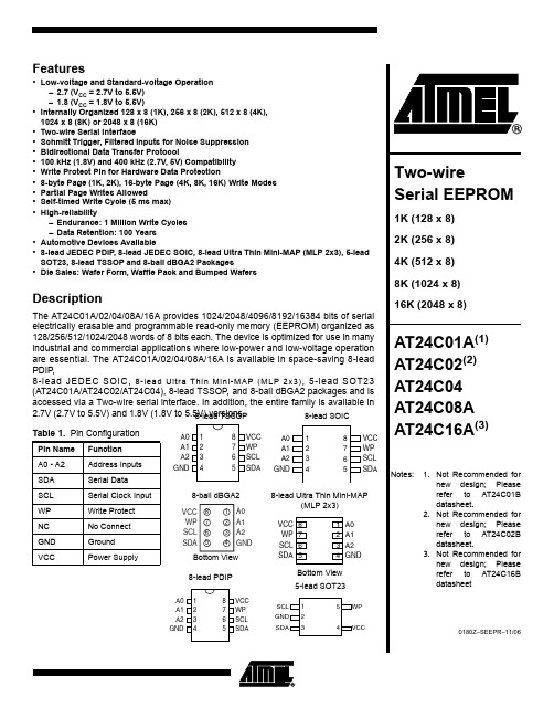
1Features•Low-voltage and Standard-voltage Operation –2.7 (V CC = 2.7V to 5.5V)–1.8 (V CC = 1.8V to 5.5V)•Internally Organized 128 x 8 (1K), 256 x 8 (2K), 512 x 8 (4K),1024 x 8 (8K) or 2048 x 8 (16K)•Two-wire Serial Interface•Schmitt Trigger, Filtered Inputs for Noise Suppression •Bidirectional Data Transfer Protocol•100 kHz (1.8V) and 400 kHz (2.7V, 5V) Compatibility •Write Protect Pin for Hardware Data Protection•8-byte Page (1K, 2K), 16-byte Page (4K, 8K, 16K) Write Modes •Partial Page Writes Allowed•Self-timed Write Cycle (5 ms max)•High-reliability–Endurance: 1 Million Write Cycles –Data Retention: 100 Years •Automotive Devices Available•8-lead JEDEC PDIP , 8-lead JEDEC SOIC, 8-lead Ultra Thin Mini-MAP (MLP 2x3), 5-lead SOT23, 8-lead TSSOP and 8-ball dBGA2 Packages•Die Sales: Wafer Form, Waffle Pack and Bumped WafersDescriptionThe AT24C01A/02/04/08A/16A provides 1024/2048/4096/8192/16384 bits of serial electrically erasable and programmable read-only memory (EEPROM) organized as 128/256/512/1024/2048 words of 8 bits each. The device is optimized for use in many industrial and commercial applications where low-power and low-voltage operation are essential. The AT24C01A/02/04/08A/16A is available in space-saving 8-lead PDIP ,8-lead JEDEC SOIC, 8-lead Ultra Thin Mini-MAP (MLP 2x3), 5-lead SOT23(AT24C01A/AT24C02/AT24C04), 8-lead TSSOP, and 8-ball dBGA2 packages and is accessed via a Two-wire serial interface. In addition, the entire family is available in 2.7V (2.7V to 5.5V) and 1.8V (1.8V to 5.5V) versions. Table 1. Pin ConfigurationPin Name Function A0 - A2Address Inputs SDA Serial Data SCL Serial Clock Input WP Write Protect NC No Connect GND Ground VCCPower Supply8-lead SOIC 8-lead PDIP8-lead Ultra Thin Mini-MAP(MLP 2x3)Bottom View 5-lead SOT238-ball dBGA2Bottom View 8-lead TSSOP2AT24C01A/02/04/08A/16A0180Z–SEEPR–11/06Figure 1. Block DiagramAbsolute Maximum RatingsOperating Temperature..................................–55°C to +125°C *NOTICE:Stresses beyond those listed under “Absolute Maximum Ratings” may cause permanent dam-age to the device. This is a stress rating only and functional operation of the device at these or any other conditions beyond those indicated in the operational sections of this specification is not implied. Exposure to absolute maximum rating conditions for extended periods may affect device reliability.Storage Temperature.....................................–65°C to +150°C Voltage on Any Pinwith Respect to Ground....................................–1.0V to +7.0V Maximum Operating Voltage..........................................6.25V DC Output Current........................................................5.0 mA3AT24C01A/02/04/08A/16A0180Z–SEEPR–11/06Pin DescriptionSERIAL CLOCK (SCL): The SCL input is used to positive edge clock data into each EEPROM device and negative edge clock data out of each device.SERIAL DATA (SDA): The SDA pin is bidirectional for serial data transfer. This pin is open-drain driven and may be wire-ORed with any number of other open-drain or open-collector devices.DEVICE/PAGE ADDRESSES (A2, A1, A0): The A2, A1 and A0 pins are device address inputs that are hard wired for the AT24C01A and the AT24C02. As many as eight 1K/2K devices may be addressed on a single bus system (device addressing is discussed in detail under the Device Addressing section).The AT24C04 uses the A2 and A1 inputs for hard wire addressing and a total of four 4K devices may be addressed on a single bus system. The A0 pin is a no connect and can be connected to ground.The AT24C08A only uses the A2 input for hardwire addressing and a total of two 8K devices may be addressed on a single bus system. The A0 and A1 pins are no connects and can be connected to ground.The AT24C16A does not use the device address pins, which limits the number of devices on a single bus to one. The A0, A1 and A2 pins are no connects and can be connected to ground.WRITE PROTECT (WP): The AT24C01A/02/04/08A/16A has a Write Protect pin that provides hardware data protection. The Write Protect pin allows normal Read/Write operations when connected to ground (GND). When the Write Protect pin is connected to V CC , the write protection feature is enabled and operates as shown in Table 2.Table 2. Write ProtectMemory OrganizationAT24C01A, 1K SERIAL EEPROM: Internally organized with 16 pages of 8 bytes each,the 1K requires a 7-bit data word address for random word addressing.AT24C02, 2K SERIAL EEPROM: Internally organized with 32 pages of 8 bytes each,the 2K requires an 8-bit data word address for random word addressing.AT24C04, 4K SERIAL EEPROM: Internally organized with 32 pages of 16 bytes each,the 4K requires a 9-bit data word address for random word addressing.AT24C08A, 8K SERIAL EEPROM: Internally organized with 64 pages of 16 bytes each, the 8K requires a 10-bit data word address for random word addressing. AT24C16A, 16K SERIAL EEPROM: Internally organized with 128 pages of 16 bytes each, the 16K requires an 11-bit data word address for random word addressing.WP Pin Status Part of the Array Protected24C01A 24C0224C0424C08A 24C16A At V CC Full (1K) ArrayFull (2K) ArrayFull (4K) ArrayFull (8K) ArrayFull (16K) ArrayAt GNDNormal Read/Write Operations4AT24C01A/02/04/08A/16A0180Z–SEEPR–11/06Note:1.This parameter is characterized and is not 100% tested.Note:1.V IL min and V IH max are reference only and are not tested.Table 3. Pin Capacitance (1)Applicable over recommended operating range from T A = 25°C, f = 1.0 MHz, V CC = +1.8VSymbol Test ConditionMax Units Conditions C I/O Input/Output Capacitance (SDA)8pF V I/O = 0V C IN Input Capacitance (A 0, A 1, A 2, SCL)6pFV IN = 0VTable 4. DC CharacteristicsApplicable over recommended operating range from: T AI = –40°C to +85°C, V CC = +1.8V to +5.5V, V CC =+1.8V to +5.5V (unless otherwise noted)Symbol Parameter Test ConditionMin TypMax Units V CC1Supply Voltage 1.8 5.5V V CC2Supply Voltage 2.7 5.5V V CC3Supply Voltage4.55.5V I CC Supply Current V CC = 5.0V READ at 100 kHz 0.4 1.0mA I CC Supply Current V CC = 5.0V WRITE at 100 kHz 2.0 3.0mA I SB1Standby Current V CC = 1.8V V IN = V CC or V SS 0.6 3.0µA I SB2Standby Current V CC = 2.5V V IN = V CC or V SS 1.4 4.0µA I SB3Standby Current V CC = 2.7V V IN = V CC or V SS 1.6 4.0µA I SB4Standby Current V CC = 5.0V V IN = V CC or V SS 8.018.0µA I LI Input Leakage Current V IN = V CC or V SS 0.10 3.0µA I LO Output Leakage Current V OUT = V CC or V SS0.05 3.0µA V IL Input Low Level (1)–0.6V CC x 0.3V V IH Input High Level (1)V CC x 0.7V CC + 0.5V V OL2Output Low Level V CC = 3.0V I OL = 2.1 mA 0.4V V OL1Output Low Level V CC = 1.8VI OL = 0.15 mA 0.2V5AT24C01A/02/04/08A/16A0180Z–SEEPR–11/06Note:1.This parameter is characterized.Table 5. AC CharacteristicsApplicable over recommended operating range from T AI = –40°C to +85°C, V CC = +1.8V to +5.5V, V CC = +2.7V to +5.5V,CL = 1 TTL Gate and 100pF (unless otherwise noted)Symbol Parameter1.8-volt2.7, 5.0-volt Units MinMax MinMax f SCL Clock Frequency, SCL 100400kHz t LOW Clock Pulse Width Low 4.7 1.2µs t HIGH Clock Pulse Width High 4.00.6µs t I Noise Suppression Time (1)10050ns t AA Clock Low to Data Out Valid 0.1 4.50.10.9µs t BUF Time the bus must be free before a new transmission can start (1) 4.7 1.2µs t HD.STA Start Hold Time 4.00.6µs t SU.STA Start Setup Time 4.70.6µs t HD.DAT Data In Hold Time 00µs t SU.DAT Data In Setup Time 200100ns t R Inputs Rise Time (1) 1.00.3µs t F Inputs Fall Time (1)300300ns t SU.STO Stop Setup Time 4.70.6µs t DH Data Out Hold Time 10050ns t WRWrite Cycle Time 55ms Endurance (1) 5.0V, 25°C, Byte Mode1M 1MWrite Cycles6AT24C01A/02/04/08A/16A0180Z–SEEPR–11/06Device OperationCLOCK and DATA TRANSITIONS: The SDA pin is normally pulled high with an exter-nal device. Data on the SDA pin may change only during SCL low time periods (see Figure 4 on page 7). Data changes during SCL high periods will indicate a start or stop condition as defined below.START CONDITION: A high-to-low transition of SDA with SCL high is a start condition which must precede any other command (see Figure 5 on page 8).STOP CONDITION: A low-to-high transition of SDA with SCL high is a stop condition.After a read sequence, the stop command will place the EEPROM in a standby power mode (see Figure 5 on page 8).ACKNOWLEDGE: All addresses and data words are serially transmitted to and from the EEPROM in 8-bit words. The EEPROM sends a zero to acknowledge that it has received each word. This happens during the ninth clock cycle.STANDBY MODE: The AT24C01A/02/04/08A/16A features a low-power standby mode which is enabled: (a) upon power-up and (b) after the receipt of the STOP bit and the completion of any internal operations.MEMORY RESET: After an interruption in protocol, power loss or system reset, any 2-wire part can be reset by following these steps:1.Clock up to 9 cycles.2.Look for SDA high in each cycle while SCL is high.3.Create a start condition.7AT24C01A/02/04/08A/16A0180Z–SEEPR–11/06Bus TimingFigure 2. SCL: Serial Clock, SDA: Serial Data I/O ®Write Cycle TimingFigure 3. SCL: Serial Clock, SDA: Serial Data I/ONote:1.The write cycle time t WR is the time from a valid stop condition of a write sequence to the end of the internal clear/write cycle.Figure 4.Data Validity8AT24C01A/02/04/08A/16A0180Z–SEEPR–11/06Figure 5. Start and Stop DefinitionFigure 6.Output Acknowledge9AT24C01A/02/04/08A/16A0180Z–SEEPR–11/06Device AddressingThe 1K, 2K, 4K, 8K and 16K EEPROM devices all require an 8-bit device address word following a start condition to enable the chip for a read or write operation (refer to Figure 7).The device address word consists of a mandatory one, zero sequence for the first four most significant bits as shown. This is common to all the EEPROM devices.The next 3 bits are the A2, A1 and A0 device address bits for the 1K/2K EEPROM.These 3 bits must compare to their corresponding hard-wired input pins.The 4K EEPROM only uses the A2 and A1 device address bits with the third bit being a memory page address bit. The two device address bits must compare to their corre-sponding hard-wired input pins. The A0 pin is no connect.The 8K EEPROM only uses the A2 device address bit with the next 2 bits being for memory page addressing. The A2 bit must compare to its corresponding hard-wired input pin. The A1 and A0 pins are no connect.The 16K does not use any device address bits but instead the 3 bits are used for mem-ory page addressing. These page addressing bits on the 4K, 8K and 16K devices should be considered the most significant bits of the data word address which follows.The A0, A1 and A2 pins are no connect.The eighth bit of the device address is the read/write operation select bit. A read opera-tion is initiated if this bit is high and a write operation is initiated if this bit is low.Upon a compare of the device address, the EEPROM will output a zero. If a compare is not made, the chip will return to a standby state.Write OperationsBYTE WRITE: A write operation requires an 8-bit data word address following the device address word and acknowledgment. Upon receipt of this address, the EEPROM will again respond with a zero and then clock in the first 8-bit data word. Following receipt of the 8-bit data word, the EEPROM will output a zero and the addressing device, such as a microcontroller, must terminate the write sequence with a stop condi-tion. At this time the EEPROM enters an internally timed write cycle, t WR , to the nonvolatile memory. All inputs are disabled during this write cycle and the EEPROM will not respond until the write is complete (see Figure 8 on page 11).PAGE WRITE: The 1K/2K EEPROM is capable of an 8-byte page write, and the 4K, 8K and 16K devices are capable of 16-byte page writes.A page write is initiated the same as a byte write, but the microcontroller does not send a stop condition after the first data word is clocked in. Instead, after the EEPROM acknowledges receipt of the first data word, the microcontroller can transmit up to seven (1K/2K) or fifteen (4K, 8K, 16K) more data words. The EEPROM will respond with a zero after each data word received. The microcontroller must terminate the page write sequence with a stop condition (see Figure 9 on page 11).The data word address lower three (1K/2K) or four (4K, 8K, 16K) bits are internally incremented following the receipt of each data word. The higher data word address bits are not incremented, retaining the memory page row location. When the word address,internally generated, reaches the page boundary, the following byte is placed at the beginning of the same page. If more than eight (1K/2K) or sixteen (4K, 8K, 16K) data words are transmitted to the EEPROM, the data word address will “roll over” and previ-ous data will be overwritten.10AT24C01A/02/04/08A/16A0180Z–SEEPR–11/06ACKNOWLEDGE POLLING: Once the internally timed write cycle has started and the EEPROM inputs are disabled, acknowledge polling can be initiated. This involves sending a start condition followed by the device address word. The read/write bit is representative of the operation desired. Only if the internal write cycle has completed will the EEPROM respond with a zero allowing the read or write sequence to continue.ReadOperationsRead operations are initiated the same way as write operations with the exception that the read/write select bit in the device address word is set to one. There are three read operations:current address read, random address read and sequential read.CURRENT ADDRESS READ: The internal data word address counter maintains the last address accessed during the last read or write operation, incremented by one. This address stays valid between operations as long as the chip power is maintained. The address “roll over” during read is from the last byte of the last memory page to the first byte of the first page.The address “roll over” during write is from the last byte of the current page to the first byte of the same page.Once the device address with the read/write select bit set to one is clocked in and acknowl-edged by the EEPROM, the current address data word is serially clocked out. The microcontroller does not respond with an input zero but does generate a following stop condi-tion (see Figure 10 on page 12).RANDOM READ: A random read requires a “dummy” byte write sequence to load in the data word address. Once the device address word and data word address are clocked in and acknowledged by the EEPROM, the microcontroller must generate another start condition.The microcontroller now initiates a current address read by sending a device address with the read/write select bit high. The EEPROM acknowledges the device address and serially clocks out the data word. The microcontroller does not respond with a zero but does generate a fol-lowing stop condition (see Figure 11 on page 12).SEQUENTIAL READ: Sequential reads are initiated by either a current address read or a ran-dom address read. After the microcontroller receives a data word, it responds with an acknowledge. As long as the EEPROM receives an acknowledge, it will continue to increment the data word address and serially clock out sequential data words. When the memory address limit is reached, the data word address will “roll over” and the sequential read will con-tinue. The sequential read operation is terminated when the microcontroller does not respond with a zero but does generate a following stop condition (see Figure 12 on page 12).11AT24C01A/02/04/08A/16A0180Z–SEEPR–11/06Figure 7. Device AddressFigure 8. Byte WriteFigure 9. Page Write(* = DON’T CARE bit for 1K)12AT24C01A/02/04/08A/16A0180Z–SEEPR–11/06Figure 10. Current Address ReadFigure 11. Random Read(* = DON’T CARE bit for 1K)Figure 12.Sequential Read13AT24C01A/02/04/08A/16A0180Z–SEEPR–11/06Notes:1.This device is not recommended for new design. Please refer to AT24C01B datasheet. For2.7V devices used in the 4.5V to5.5V range, please refer to performance values in the AC and DC characteristics table.2.“U” designates Green Package + RoHS compliant.3.“H” designates Green Package + RoHS compliant, with NiPdAu Lead Finish.4.Available in waffle pack and wafer form; order as SL788 for inkless wafer form. Bumped die available upon request. Pleasecontact Serial EEPROM Marketing.AT24C01A Ordering Information (1)Ordering CodePackage Operation RangeAT24C01A-10PU-2.7(2)AT24C01A-10PU-1.8(2)AT24C01A-10SU-2.7(2)AT24C01A-10SU-1.8(2)AT24C01A-10TU-2.7(2)AT24C01A-10TU-1.8(2)AT24C01A-10TSU-1.8(2)AT24C01AU3-10UU-1.8(2)AT24C01AY1-10YU-1.8(2) (Not recommended for new design)AT24C01AY6-10YH-1.8(3)8P38P38S18S18A28A25TS18U318Y18Y6Lead-free/Halogen-free/Industrial Temperature (–40°C to 85°C)AT24C01A-W1.8-11(4)Die SaleIndustrial Temperature (–40°C to 85°C)Package Type8P38-lead, 0.300" Wide, Plastic Dual Inline Package (PDIP)8S18-lead, 0.150" Wide, Plastic Gull Wing Small Outline (JEDEC SOIC)8A28-lead, 4.4 mm Body, Plastic Thin Shrink Small Outline Package (TSSOP)8Y18-lead, 4.90 mm x 3.00 mm Body, Dual Footprint, Non-leaded, Miniature Array Package (MAP)8Y68-lead, 2.00 x 3.00 mm Body, 0.50 mm Pitch, Ultra Thin Mini-MAP , Dual No Lead Package (DFN), (MLP 2x3 mm)5TS15-lead, 2.90 mm x 1.60 mm Body, Plastic Thin Shrink Small Outline Package (SOT23)8U3-18-ball, die Ball Grid Away Package (dBGA2)Options–2.7Low-voltage (2.7V to 5.5V)–1.8Low-voltage (1.8V to 5.5V)14AT24C01A/02/04/08A/16A0180Z–SEEPR–11/06Notes:1.This device is not recommended for new design. Please refer to AT24C02B datasheet. For2.7V devices used in the 4.5V to5.5V range, please refer to performance values in the AC and DC characteristics table.2.“U” designates Green Package + RoHS compliant.3.Available in waffle pack and wafer form; order as SL719 for wafer form. Bumped die available upon request. Please contactSerial EEPROM Marketing.AT24C02 Ordering Information (1)Ordering Code Package Operation RangeAT24C02-10PU-2.7(2)AT24C02-10PU-1.8(2)AT24C02N-10SU-2.7(2)AT24C02N-10SU-1.8(2)AT24C02-10TU-2.7(2)AT24C02-10TU-1.8(2)AT24C02Y1-10YU-1.8(2)AT24C02-10TSU-1.8(2)AT24C02U3-10UU-1.8(2)8P38P38S18S18A28A28Y15TS18U3-1Lead-free/Halogen-free/Industrial Temperature (–40°C to 85°C)AT24C02-W2.7-11(3)Die SaleIndustrial Temperature (–40°C to 85°C)Package Type8P38-lead, 0.300" Wide, Plastic Dual Inline Package (PDIP)8S18-lead, 0.150" Wide, Plastic Gull Wing Small Outline (JEDEC SOIC)8A28-lead, 4.4 mm Body, Plastic Thin Shrink Small Outline Package (TSSOP)8Y18-lead, 4.90 mm x 3.00 mm Body, Dual Footprint, Non-leaded, Miniature Array Package (MAP)5TS15-lead, 2.90 mm x 1.60 mm Body, Plastic Thin Shrink Small Outline Package (SOT23)8U3-18-ball, die Ball Grid Away Package (dBGA2)Options–2.7Low-voltage (2.7V to 5.5V)–1.8Low-voltage (1.8V to 5.5V)15AT24C01A/02/04/08A/16A0180Z–SEEPR–11/06Notes:1.For2.7V devices used in the 4.5V to 5.5V range, please refer to performance values in the AC and DC characteristics table.2.“U” designates Green Package + RoHS compliant.3.“H” designates Green Package + RoHS compliant, with NiPdAu Lead Finish.4.Available in waffle pack and wafer form; order as SL788 for inkless wafer form. Bumped die available upon request. Please contact Serial EEPROM Marketing.AT24C04 Ordering Information (1)Ordering CodePackage Operation RangeAT24C04-10PU-2.7(2)AT24C04-10PU-1.8(2)AT24C04N-10SU-2.7(2)AT24C04N-10SU-1.8(2)AT24C04-10TU-2.7(2)AT24C04-10TU-1.8(2)AT24C04Y1-10YU-1.8(2) (Not recommended for new design)AT24C04Y6-10YH-1.8(3)AT24C04-10TSU-1.8(2)AT24C04U3-10UU-1.8(2)8P38P38S18S18A28A28Y18Y65TS18U3-1Lead-free/Halogen-free/Industrial Temperature (–40°C to 85°C)AT24C04-W1.8-11(4)Die SaleIndustrial Temperature (–40°C to 85°C)Package Type8P38-lead, 0.300" Wide, Plastic Dual Inline Package (PDIP)8S18-lead, 0.150" Wide, Plastic Gull Wing Small Outline (JEDEC SOIC)8A28-lead, 4.4 mm Body, Plastic Thin Shrink Small Outline Package (TSSOP)8Y18-lead, 4.90 mm x 3.00 mm Body, Dual Footprint, Non-leaded, Miniature Array Package (MAP)8Y68-lead, 2.00 x 3.00 mm Body, 0.50 mm Pitch, Ultra Thin Mini-MAP , Dual No Lead Package (DFN), (MLP 2x3 mm)5TS15-lead, 2.90 mm x 1.60 mm Body, Plastic Thin Shrink Small Outline Package (SOT23)8U3-18-ball, die Ball Grid Away Package (dBGA2)Options–2.7Low-voltage (2.7V to 5.5V)–1.8Low-voltage (1.8V to 5.5V)16AT24C01A/02/04/08A/16A0180Z–SEEPR–11/06Notes:1.For2.7V devices used in the 4.5V to 5.5V range, please refer to performance values in the AC and DC characteristics table.2.“U” designates Green Package + RoHS compliant.3.“H” designates Green Package + RoHS compliant, with NiPdAu Lead Finish.4.Available in waffle pack and wafer form; order as SL788 for inkless wafer form. Bumped die available upon request. Please contact Serial EEPROM Marketing.AT24C08A Ordering Information (1)Ordering CodePackage Operation RangeAT24C08A-10PU-2.7(2)AT24C08A-10PU-1.8(2)AT24C08AN-10SU-2.7(2)AT24C08AN-10SU-1.8(2)AT24C08A-10TU-2.7(2)AT24C08A-10TU-1.8(2)AT24C08AY1-10YU-1.8(2) (Not recommended for new design)AT24C08AY6-10YH-1.8(3)AT24C08AU2-10UU-1.8(28P38P38S18S18A28A28Y18Y68U2-1Lead-free/Halogen-free/Industrial Temperature (−40°C to 85°C)AT24C08A-W1.8-11(4)Die SaleIndustrial Temperature (–40°C to 85°C)Package Type8P38-pin, 0.300" Wide, Plastic Dual Inline Package (PDIP)8S18-lead, 0.150" Wide, Plastic Gull Wing Small Outline (JEDEC SOIC)8A28-lead, 4.4 mm Body, Plastic Thin Shrink Small Outline Package (TSSOP)8Y18-lead, 4.90 mm x 3.00 mm Body, Dual Footprint, Non-leaded, Miniature Array Package (MAP)8Y68-lead, 2.00 x 3.00 mm Body, 0.50 mm Pitch, Ultra Thin Mini-MAP , Dual No Lead Package (DFN), (MLP 2x3 mm)8U2-18-ball, die Ball Grid Array Package (dBGA2)Options−2.7Low Voltage (2.7V to 5.5V)−1.8Low Voltage (1.8V to 5.5V)17AT24C01A/02/04/08A/16A0180Z–SEEPR–11/06Notes:1.This device is not recommended for new design. Please refer to AT24C16B datasheet. For2.7V devices used in the 4.5V to5.5V range, please refer to performance values in the AC and DC characteristics table.2.“U” designates Green Package + RoHS compliant.3.“H” designates Green Package + RoHS compliant, with NiPdAu Lead Finish.4.Available in waffle pack and wafer form; order as SL788 for inkless wafer form. Bumped die available upon request. Pleasecontact Serial EEPROM Marketing.AT24C16A Ordering Information (1)Ordering CodePackage Operation RangeAT24C16A-10PU-2.7(2)AT24C16A-10PU-1.8(2)AT24C16AN-10SU-2.7(2)AT24C16AN-10SU-1.8(2)AT24C16A-10TU-2.7(2)AT24C16A-10TU-1.8(2)AT24C16AY1-10YU-1.8(2) (Not recommended for new design)AT24C16AY6-10YH-1.8(3)AT24C16AU2-10UU-1.8(2)8P38P38S18S18A28A28Y18Y68U2-1Lead-free/Halogen-free/Industrial Temperature (−40°C to 85°C)AT24C16A-W1.8-11(3)Die SaleIndustrial Temperature (−40°C to 85°C)Package Type8P38-pin, 0.300" Wide, Plastic Dual Inline Package (PDIP)8S18-lead, 0.150" Wide, Plastic Gull Wing Small Outline (JEDEC SOIC)8A28-lead, 0.170" Wide, Thin Shrink Small Outline Package (TSSOP)8Y18-lead, 4.90 mm x 3.00 mm Body, Dual Footprint, Non-leaded, Miniature Array Package (MAP)8Y68-lead, 2.00 x 3.00 mm Body, 0.50 mm Pitch, Ultra Thin Mini-MAP , Dual No Lead Package (DFN), (MLP 2x3 mm)8U2-18-ball, die Ball Grid Array Package (dBGA2)Options−2.7Low Voltage (2.7V to 5.5V)−1.8Low Voltage (1.8V to 5.5V)18AT24C01A/02/04/08A/16A0180Z–SEEPR–11/06Packaging Information8P3 – PDIP19AT24C01A/02/04/08A/16A0180Z–SEEPR–11/068S1 – JEDEC SOIC20AT24C01A/02/04/08A/16A0180Z–SEEPR–11/068A2 – TSSOP21AT24C01A/02/04/08A/16A0180Z–SEEPR–11/068Y1 – MAP22AT24C01A/02/04/08A/16A0180Z–SEEPR–11/068Y6 − Mini-MAP (MLP 2x3 mm)23AT24C01A/02/04/08A/16A0180Z–SEEPR–11/065TS1 – SOT2324AT24C01A/02/04/08A/16A0180Z–SEEPR–11/068U2 – dBGA225AT24C01A/02/04/08A/16A0180Z–SEEPR–11/068U3-1 – dBGA20180Z–SEEPR–11/06Disclaimer: The information in this document is provided in connection with Atmel products. No license, express or implied, by estoppel or otherwise,to any intellectual property right is granted by this document or in connection with the sale of Atmel products. EXCEPT AS SET FORTH IN ATMEL’S TERMS AND CONDI-TIONS OF SALE LOCATED ON ATMEL’S WEB SITE, ATMEL ASSUMES NO LIABILITY WHATSOEVER AND DISCLAIMS ANY EXPRESS, IMPLIED OR STATUTORY WARRANTY RELATING TO ITS PRODUCTS INCLUDING, BUT NOT LIMITED TO, THE IMPLIED WARRANTY OF MERCHANTABILITY, FITNESS FOR A PARTICULAR PURPOSE, OR NON-INFRINGEMENT. IN NO EVENT SHALL ATMEL BE LIABLE FOR ANY DIRECT, INDIRECT, CONSEQUENTIAL, PUNITIVE, SPECIAL OR INCIDEN-TAL DAMAGES (INCLUDING, WITHOUT LIMITATION, DAMAGES FOR LOSS OF PROFITS, BUSINESS INTERRUPTION, OR LOSS OF INFORMATION) ARISING OUT OF THE USE OR INABILITY TO USE THIS DOCUMENT, EVEN IF ATMEL HAS BEEN ADVISED OF THE POSSIBILITY OF SUCH DAMAGES. Atmel makes no representations or warranties with respect to the accuracy or completeness of the contents of this document and reserves the right to make changes to specifications and product descriptions at any time without notice. Atmel does not make any commitment to update the information contained herein. Unless specifically provided otherwise, Atmel products are not suitable for, and shall not be used in, automotive applications. Atmel’s products are not intended, authorized, or warranted for use as components in applications intended to support or sustain life.Atmel CorporationAtmel Operations2325 Orchard Parkway San Jose, CA 95131, USA Tel: 1(408) 441-0311Fax: 1(408) 487-2600Regional HeadquartersEuropeAtmel SarlRoute des Arsenaux 41Case Postale 80CH-1705 Fribourg SwitzerlandTel: (41) 26-426-5555Fax: (41) 26-426-5500AsiaRoom 1219Chinachem Golden Plaza 77 Mody Road Tsimshatsui East Kowloon Hong KongTel: (852) 2721-9778Fax: (852) 2722-1369Japan9F, Tonetsu Shinkawa Bldg.1-24-8 ShinkawaChuo-ku, Tokyo 104-0033JapanTel: (81) 3-3523-3551Fax: (81) 3-3523-7581Memory2325 Orchard Parkway San Jose, CA 95131, USA Tel: 1(408) 441-0311Fax: 1(408) 436-4314Microcontrollers2325 Orchard Parkway San Jose, CA 95131, USA Tel: 1(408) 441-0311Fax: 1(408) 436-4314La Chantrerie BP 7060244306 Nantes Cedex 3, France Tel: (33) 2-40-18-18-18Fax: (33) 2-40-18-19-60ASIC/ASSP/Smart CardsZone Industrielle13106 Rousset Cedex, France Tel: (33) 4-42-53-60-00Fax: (33) 4-42-53-60-011150 East Cheyenne Mtn. Blvd.Colorado Springs, CO 80906, USA Tel: 1(719) 576-3300Fax: 1(719) 540-1759Scottish Enterprise Technology Park Maxwell BuildingEast Kilbride G75 0QR, Scotland Tel: (44) 1355-803-000Fax: (44) 1355-242-743RF/AutomotiveTheresienstrasse 2Postfach 353574025 Heilbronn, Germany Tel: (49) 71-31-67-0Fax: (49) 71-31-67-23401150 East Cheyenne Mtn. Blvd.Colorado Springs, CO 80906, USA Tel: 1(719) 576-3300Fax: 1(719) 540-1759Biometrics/Imaging/Hi-Rel MPU/High Speed Converters/RF DatacomAvenue de Rochepleine BP 12338521 Saint-Egreve Cedex, France Tel: (33) 4-76-58-30-00Fax: (33) 4-76-58-34-80Literature Requests/literature© 2006 Atmel Corporation. All rights reserved. Atmel ®, logo and combinations thereof, Everywhere You Are ® and others, are registered trade-marks or trademarks of Atmel Corporation or its subsidiaries. Other terms and product names may be trademarks of others.。
Atmel改变命名规则的芯片型号对照表
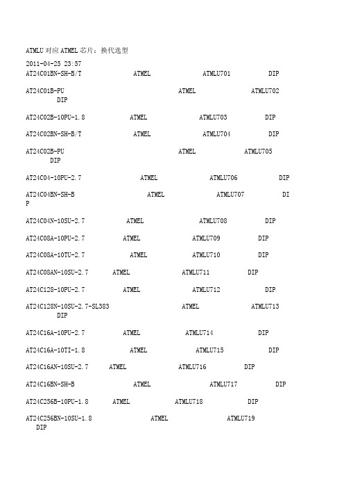
ATMLU对应ATMEL芯片:换代选型2011-04-25 23:57AT24C01BN-SH-B/T ATMEL ATMLU701 DIPAT24C01B-PU ATMEL ATMLU702 DIPAT24C02B-10PU-1.8 ATMEL ATMLU703 DIPAT24C02BN-SH-B/T ATMEL ATMLU704 DIPAT24C02B-PU ATMEL ATMLU705 DIPAT24C04-10PU-2.7 ATMEL ATMLU706 DIPAT24C04BN-SH-B ATMEL ATMLU707 DI PAT24C04N-10SU-2.7 ATMEL ATMLU708 DIPAT24C08A-10PU-2.7 ATMEL ATMLU709 DIPAT24C08A-10TU-2.7 ATMEL ATMLU710 DIPAT24C08AN-10SU-2.7 ATMEL ATMLU711 DIPAT24C128-10PU-2.7 ATMEL ATMLU712 DIPAT24C128N-10SU-2.7-SL383 ATMEL ATMLU713 DIPAT24C16A-10PU-2.7 ATMEL ATMLU714 DIPAT24C16A-10TI-1.8 ATMEL ATMLU715 DIP AT24C16AN-10SU-2.7 ATMEL ATMLU716 DIPAT24C16BN-SH-B ATMEL ATMLU717 DIP AT24C256B-10PU-1.8 ATMEL ATMLU718 DIPAT24C256BN-10SU-1.8 ATMEL ATMLU719DIPAT24C256BN-SH-T ATMEL ATMLU720 DIPAT24C256B-PU ATMELATMLU721 DIPAT24C256N-10SI18 ATMEL ATMLU722 DIPAT24C32A-10PU-2.7 ATMEL ATMLU723 DIPAT24C32AN-10SU-2.7 ATMEL ATMLU724 DIPAT24C32CN-SH-T ATMEL ATMLU72 5 DIPAT24C512-10PU-2.7 ATMEL ATMLU726 DIPAT24C512BN-SH25-B ATMEL ATMLU727 DIPAT24C512BN-SH-B ATMEL ATMLU728 DIPAT24C512B-PU25 ATMEL ATMLU7 29 DIPAT24C512N-10SU-2.7 ATMEL ATMLU730 DIPAT24C64A-10PU-2.7 ATMEL ATMLU731 DIPAT24C64AN-10SU-2.7 ATMEL ATMLU732 DIPAT24C64CN-SH-B ATMEL ATMLU7 33 DIPAT24C64CN-SH-T ATMEL ATMLU73 4 DIPAT25128A-10PU-2.7 ATMEL ATMLU735 DIPAT25256AN-10SU-2.7 ATMEL ATMLU736 DIPAT25DF041A-SH-B ATMEL ATMLU737 DIPAT25F1024AN-10SU-2.7-SL383 ATMELATMLU738 DIPAT25F512AN-10SU-2.7-SL383 ATMELATMLU739 DIPAT26DF081A-SSU-SL965 ATMELATMLU740 DIPAT26DF081A-SU-SL965 ATME L ATMLU741 DIPAT26DF161-SUATMEL ATMLU742 DIPAT26DF321-SU ATMELATMLU743 DIPAT27BV256-70JU ATMEL ATMLU744 DIPAT27C010-70PU ATMEL ATMLU74 5 DIPAT27C040-70PU ATMEL ATMLU746DIPAT27C256R-70JU ATMEL ATMLU747DIPAT27C256R-70PU ATMEL ATMLU748DIPAT27C512R-70JU ATMEL ATMLU749 DIPAT28BV256-20TU ATMEL ATMLU750 DIPAT28C256-15PU ATMEL ATMLU751 DIPAT28C64B-15JU ATMEL ATMLU752 DIPAT28C64B-15PU ATMEL ATMLU801 DIPAT28C64B-15SU ATMEL ATMLU802 DIPAT29C010A-70JU ATMEL ATMLU803 DIPAT29C020-90JU ATMEL ATMLU80 4 DIPAT29C020-90TU ATMEL ATMLU805 DIPAT29C040A-90JU ATMEL ATMLU806 DIPAT29C040A-90TU ATMEL ATMLU807DIPAT29LV020-10TU ATMEL ATMLU808 DIPAT29LV040A-15JU ATMEL ATMLU809 DIPAT29LV512-12JU ATMEL ATMLU810 DIPAT45DB021B-SU ATMEL ATMLU811 DIPAT45DB041D-SU ATMEL ATMLU812 DIPAT45DB081D-SU ATMEL ATMLU813 DIPAT45DB161D-SU ATMEL ATMLU814 DIPAT45DB161D-TU ATMEL ATMLU815 DIPAT45DB321D-SU ATMEL ATMLU816 DIPAT45DB321D-TU ATMEL ATMLU817 DIPAT45DB642D-TU ATMEL ATMLU818 DIPAT47BV163A-70TU ATMEL ATMLU819 DIPAT49BV040B-JU ATMEL ATMLU820 DIPAT49BV322DT-70TU ATMEL ATMLU821 DIPAT49BV512-90TU ATMEL ATMLU822 DIPAT73C213 ATMEL ATMLU823 DIPAT76C112 ATMEL ATMLU824 DIPAT76C120H-MU1-JZ208 ATMEL ATMLU825 DIPAT80251G2D-SLSUM ATMEL ATMLU826 DIPAT80C32X2-3CSUM ATMEL ATMLU827 DIPAT80C32X2-RLTUM ATMEL ATMLU828 DIPAT80C32X2-SLSUM ATMEL ATMLU829 DIPAT83C24-TISIL ATMEL ATMLU830 DIPAT88SC0104C-SU ATMEL ATMLU831 DIPAT88SC153-10SU ATMEL ATMLU832 DIPAT89C2051-12PU ATMEL ATMLU833 DIPAT89C2051-24PU ATMEL ATMLU835 DIPAT89C2051-24SU ATMEL ATMLU836 DIPAT89C4051-24PU ATMEL ATMLU837 DIPAT89C4051-24SU ATMEL ATMLU838 DIPAT89C5131A-S3SUM ATMEL ATMLU839 DIP AT89C51AC2-RLTUM ATMEL ATMLU840 DIP AT89C51CC01CA-RLTUM ATMEL ATMLU841 DIP AT89C51CC01CA-SLSUM ATMEL ATMLU842 DIP AT89C51CC01UA-RLTUM ATMEL ATMLU843 DIP AT89C51CC01UA-SLSUM ATMEL ATMLU844 DIP AT89C51ED2-RDTUM ATMEL ATMLU845 DIP AT89C51ED2-RLTUM ATMEL ATMLU846 DIP AT89C51ED2-SLSUM ATMEL ATMLU847 DIP AT89C51ED2-SMSUM ATMEL ATMLU848 DIP AT89C51RB2-3CSUM ATMEL ATMLU849 DIP AT89C51RB2-RLTUM ATMEL ATMLU850 DIP AT89C51RB2-SLSUM ATMEL ATMLU851 DIP AT89C51RC2-3CSUM ATMEL ATMLU852 DIP AT89C51RC-24JU ATMEL ATMLU901 DIPAT89C51RC-24PU ATMEL ATMLU902 DIPAT89C51RC2-RLTUM ATMEL ATMLU903 DIP AT89C51RC2-SLSUM ATMEL ATMLU904 DIPAT89C51RD2-SLRUM ATMEL ATMLU906 DIP AT89C51RD2-SLSUM ATMEL ATMLU907 DIP AT89C51-24PC ATMEL ATMLU908 DIPAT89C51-24PI ATMEL ATMLU909 DIPAT89C52-24JI ATMEL ATMLU910 DIPAT89C52-24PI ATMEL ATMLH701 SOPAT89C55WD-24AU ATMEL ATMLH702 SOP AT89C55WD-24JU ATMEL ATMLH703 SOP AT89C55WD-24PU ATMEL ATMLH704 SOP AT89LS52-16JU ATMEL ATMLH705 SOP AT89LS52-16PU ATMEL ATMLH706 SOP AT89LV51-12AI ATMEL ATMLH707 SOP AT89S51-24AU ATMEL ATMLH708 SOPAT89S51-24PU ATMEL ATMLH709 SOPAT89S52-24AU ATMEL ATMLH710 SOPAT89S52-24JU ATMEL ATMLH711 SOPAT89S52-24PU ATMEL ATMLH712 SOPAT89S54-3CSIM ATMEL ATMLH713 SOP AT89S54-SLSIM ATMEL ATMLH714 SOP AT89S58-SLSIM ATMEL ATMLH715 SOP AT89S8253-24AU ATMEL ATMLH716 SOP AT89S8253-24JU ATMEL ATMLH717 SOPAT90CAN128-16AU ATMEL ATMLH719 SOPAT90CAN32-16AU ATMEL ATMLH720 SOPAT91M40800-33AU ATMEL ATMLH721 SOPAT91M55800A-33AU ATMEL ATMLH722 SOP AT91RM9200-CJ-002 ATMEL ATMLH723 SOP AT91RM9200-QU-002 ATMEL ATMLH724 SOP AT91SAM7S256-AU-001 ATMEL ATMLH725 SOP AT91SAM7S321-AU ATMEL ATMLH726 SOPAT91SAM7S32-AU-001 ATMEL ATMLH727 SOP AT91SAM7S64-AU-001 ATMEL ATMLH728 SOP AT91SAM7SE32-AU ATMEL ATMLH729 SOPAT91SAM7X256-AU ATMEL ATMLH730 SOPAT91SAM9260-CJ ATMEL ATMLH731 SOPAT91SAM9260-EK ATMEL ATMLH732 SOPAT91SAM9261-EK ATMEL ATMLH733 SOPAT91SAM9261S-CU ATMEL ATMLH734 SOPAT91SAM9263-CU ATMEL ATMLH735 SOPAT91SAM7X-EK ATMEL ATMLH736 SOPAT91SAM-ICE ATMEL ATMLH737 SOPAT93C46-10PU-2.7 ATMEL ATMLH738 SOP AT93C46-10SU-2.7 ATMEL ATMLH739 SOP AT93C46DN-SH-B ATMEL ATMLH740 SOPAT93C56A-10PU-2.7 ATMEL ATMLH742 SOPAT93C56A-10SU-2.7 ATMEL ATMLH743 SOPAT93C66A-10PU27 ATMEL ATMLH744 SOPAT93C66A-10SU-2.7 ATMEL ATMLH745 SOPAT93C66A-10SU-2.7-SL383 ATMEL ATMLH746 SOP ATAVRDRAGON ATMEL ATMLH747 SOPATAVRISP2 ATMEL ATMLH748 SOPATF1502AS-15JC44 ATMEL ATMLH749 SOPATF1508AS-15AC100 ATMEL ATMLH750 SOPATF1508AS-15JC84 ATMEL ATMLH751 SOPATF16V8B-15JU ATMEL ATMLH752 SOPATF16V8B-15PC ATMEL ATMLH801 SOPATF16V8B-15PU ATMEL ATMLH802 SOPATF16V8BQL-15JC ATMEL ATMLH803 SOPATF20V8B-15JC ATMEL ATMLH804 SOP ATJTAGICE2 ATMEL ATMLH805 SOPATMEGA1280V-8AU ATMEL ATMLH806 SOP ATMEGA128-16AU ATMEL ATMLH807 SOP ATMEGA128L-8AU ATMEL ATMLH808 SOP ATMEGA16-16AU ATMEL ATMLH809 SOPATMEGA16-16PU ATMEL ATMLH810 SOPATMEGA162-16PU ATMEL ATMLH811 SOPATMEGA168-20AU ATMEL ATMLH813 SOP ATMEGA168-20MU ATMEL ATMLH814 SOP ATMEGA168-20PU ATMEL ATMLH815 SOP ATMEGA168V-10AU ATMEL ATMLH816 SOP ATMEGA169P-16AU ATMEL ATMLH817 SOP ATMEGA169PV-8AU ATMEL ATMLH818 SOP ATMEGA169V-8AU ATMEL ATMLH819 SOP ATMEGA16L-8AU ATMEL ATMLH820 SOP ATMEGA16L-8PU ATMEL ATMLH821 SOP ATMEGA32-16AU ATMEL ATMLH822 SOP ATMEGA32-16PU ATMEL ATMLH823 SOP ATMEGA325V-8MU ATMEL ATMLH824 SOP ATMEGA32L-8AU ATMEL ATMLH825 SOP ATMEGA32L-8PU ATMEL ATMLH826 SOP ATMEGA48-20AU ATMEL ATMLH827 SOP ATMEGA48V-10AU ATMEL ATMLH828 SOP ATMEGA48V-10PU ATMEL ATMLH829 SOP ATMEGA48V-10MU ATMEL ATMLH830 SOP ATMEGA640V-8AU ATMEL ATMLH831 SOP ATMEGA64-16AU ATMEL ATMLH832 SOP ATMEGA64L-8AU ATMEL ATMLH833 SOP ATMEGA8-16AU ATMEL ATMLH834 SOPATMEGA8515-16AU ATMEL ATMLH836 SOP ATMEGA8515-16JU ATMEL ATMLH837 SOP ATMEGA8515-16PU ATMEL ATMLH838 SOP ATMEGA8515L-8JU ATMEL ATMLH839 SOP ATMEGA8535-16JI ATMEL ATMLH840 SOP ATMEGA8535-16JU ATMEL ATMLH841 SOP ATMEGA8535-16PU ATMEL ATMLH842 SOP ATMEGA8535L-8AU ATMEL ATMLH843 SOP ATMEGA8535L-8JU ATMEL ATMLH844 SOP ATMEGA8535L-8PU ATMEL ATMLH845 SOP ATMEGA88-20AU ATMEL ATMLH846 SOP ATMEGA88-20MU ATMEL ATMLH847 SOP ATMEGA88-20PU ATMEL ATMLH848 SOP ATMEGA88V-10AU ATMEL ATMLH849 SOP ATMEGA88V-10MU ATMEL ATMLH850 SOP ATMEGA88V-10PU ATMEL ATMLH851 SOP ATMEGA8L-8AU ATMEL ATMLH852 SOP ATMEGA8L-8PU ATMEL ATMLH901 SOP ATTINY11L-2SU ATMEL ATMLH902 SOP ATTINY13-20SU ATMEL ATMLH903 SOP ATTINY13V-10PU ATMEL ATMLH904 SOP ATTINY13V-10SSU ATMEL ATMLH905 SOPATTINY15L-1PU ATMEL ATMLH907 SOPATTINY2313-20PU ATMEL ATMLH908 SOPATTINY2313-20SU ATMEL ATMLH909 SOPATTINY2313V-10PU ATMEL ATMLH910 SOPAT24C01BN-SH-B/T ATMEL ATMLU701 DIPAT24C01B-PI ATMEL ATMLU702 DIPAT24C02B-10PI-1.8 ATMEL ATMLU703 DIPAT24C02BN-SH-B/T ATMEL ATMLU704 DIPAT24C02B-PI ATMEL ATMLU705 DIPAT24C04-10PI-2.7 ATMEL ATMLU706 DIPAT24C04BN-SH-B ATMEL ATMLU707 DIPAT24C04N-10SI-2.7 ATMEL ATMLU708 DIPAT24C08A-10PI-2.7 ATMEL ATMLU709 DIPAT24C08A-10TI-2.7 ATMEL ATMLU710 DIPAT24C08AN-10SI-2.7 ATMEL ATMLU711 DIPAT24C128-10PI-2.7 ATMEL ATMLU712 DIPAT24C128N-10SI-2.7-SL383 ATMEL ATMLU713 DIP AT24C16A-10PI-2.7 ATMEL ATMLU714 DIPAT24C16A-10TI-1.8 ATMEL ATMLU715 DIPAT24C16AN-10SI-2.7 ATMEL ATMLU716 DIPAT24C16BN-SH-B ATMEL ATMLU717 DIPAT24C256B-10PI-1.8 ATMEL ATMLU718 DIPAT24C256BN-10SI-1.8 ATMEL ATMLU719 DIPAT24C256BN-SH-T ATMEL ATMLU720 DIPAT24C256B-PI ATMEL ATMLU721 DIPAT24C256N-10SI18 ATMEL ATMLU722 DIPAT24C32A-10PI-2.7 ATMEL ATMLU723 DIPAT24C32AN-10SI-2.7 ATMEL ATMLU724 DIPAT24C32CN-SH-T ATMEL ATMLU725 DIPAT24C512-10PI-2.7 ATMEL ATMLU726 DIPAT24C512BN-SH25-B ATMEL ATMLU727 DIPAT24C512BN-SH-B ATMEL ATMLU728 DIPAT24C512B-PI25 ATMEL ATMLU729 DIPAT24C512N-10SI-2.7 ATMEL ATMLU730 DIPAT24C64A-10PI-2.7 ATMEL ATMLU731 DIPAT24C64AN-10SI-2.7 ATMEL ATMLU732 DIPAT24C64CN-SH-B ATMEL ATMLU733 DIPAT24C64CN-SH-T ATMEL ATMLU734 DIPAT25128A-10PI-2.7 ATMEL ATMLU735 DIPAT25256AN-10SI-2.7 ATMEL ATMLU736 DIPAT25DF041A-SH-B ATMEL ATMLU737 DIPAT25F1024AN-10SI-2.7-SL383 ATMEL ATMLU738 DIP AT25F512AN-10SI-2.7-SL383 ATMEL ATMLU739 DIP AT26DF081A-SSI-SL965 ATMEL ATMLU740 DIPAT26DF081A-SI-SL965 ATMEL ATMLU741 DIPAT26DF321-SI ATMEL ATMLU743 DIP AT27BV256-70JI ATMEL ATMLU744 DIP AT27C010-70PI ATMEL ATMLU745 DIP AT27C040-70PI ATMEL ATMLU746 DIP AT27C256R-70JI ATMEL ATMLU747 DIP AT27C256R-70PI ATMEL ATMLU748 DIP AT27C512R-70JI ATMEL ATMLU749 DIP AT28BV256-20TI ATMEL ATMLU750 DIP AT28C256-15PI ATMEL ATMLU751 DIP AT28C64B-15JI ATMEL ATMLU752 DIP AT28C64B-15PI ATMEL ATMLU801 DIP AT28C64B-15SI ATMEL ATMLU802 DIP AT29C010A-70JI ATMEL ATMLU803 DIP AT29C020-90JI ATMEL ATMLU804 DIP AT29C020-90TI ATMEL ATMLU805 DIP AT29C040A-90JI ATMEL ATMLU806 DIP AT29C040A-90TI ATMEL ATMLU807 DIP AT29LV020-10TI ATMEL ATMLU808 DIP AT29LV040A-15JI ATMEL ATMLU809 DIP AT29LV512-12JI ATMEL ATMLU810 DIP AT45DB021B-SI ATMEL ATMLU811 DIP AT45DB041D-SI ATMEL ATMLU812 DIPAT45DB161D-SI ATMEL ATMLU814 DIPAT45DB161D-TI ATMEL ATMLU815 DIPAT45DB321D-SI ATMEL ATMLU816 DIPAT45DB321D-TI ATMEL ATMLU817 DIPAT45DB642D-TI ATMEL ATMLU818 DIPAT47BV163A-70TI ATMEL ATMLU819 DIPAT49BV040B-JI ATMEL ATMLU820 DIPAT49BV322DT-70TI ATMEL ATMLU821 DIP AT49BV512-90TI ATMEL ATMLU822 DIPAT73C213 ATMEL ATMLU823 DIPAT76C112 ATMEL ATMLU824 DIPAT76C120H-MI1-JZ208 ATMEL ATMLU825 DIP AT80251G2D-SLSIM ATMEL ATMLU826 DIP AT80C32X2-3CSIM ATMEL ATMLU827 DIPAT80C32X2-RLTIM ATMEL ATMLU828 DIPAT80C32X2-SLSIM ATMEL ATMLU829 DIPAT83C24-TISIL ATMEL ATMLU830 DIPAT88SC0104C-SI ATMEL ATMLU831 DIPAT88SC153-10SI ATMEL ATMLU832 DIPAT89C2051-12PI ATMEL ATMLU833 DIPAT89C2051-12SI ATMEL ATMLU834 DIPAT89C2051-24PI ATMEL ATMLU835 DIPAT89C4051-24PI ATMEL ATMLU837 DIPAT89C4051-24SI ATMEL ATMLU838 DIPAT89C5131A-S3SIM ATMEL ATMLU839 DIP AT89C51AC2-RLTIM ATMEL ATMLU840 DIP AT89C51CC01CA-RLTIM ATMEL ATMLU841 DIP AT89C51CC01CA-SLSIM ATMEL ATMLU842 DIP AT89C51CC01IA-RLTIM ATMEL ATMLU843 DIP AT89C51CC01IA-SLSIM ATMEL ATMLU844 DIP AT89C51ED2-RDTIM ATMEL ATMLU845 DIP AT89C51ED2-RLTIM ATMEL ATMLU846 DIP AT89C51ED2-SLSIM ATMEL ATMLU847 DIP AT89C51ED2-SMSIM ATMEL ATMLU848 DIP AT89C51RB2-3CSIM ATMEL ATMLU849 DIP AT89C51RB2-RLTIM ATMEL ATMLU850 DIP AT89C51RB2-SLSIM ATMEL ATMLU851 DIP AT89C51RC2-3CSIM ATMEL ATMLU852 DIP AT89C51RC-24JI ATMEL ATMLU901 DIPAT89C51RC-24PI ATMEL ATMLU902 DIPAT89C51RC2-RLTIM ATMEL ATMLU903 DIP AT89C51RC2-SLSIM ATMEL ATMLU904 DIP AT89C51RD2-RLTIM ATMEL ATMLU905 DIP AT89C51RD2-SLRIM ATMEL ATMLU906 DIPAT89C51-24PC ATMEL ATMLU908 DIP AT89C51-24PI ATMEL ATMLU909 DIP AT89C52-24JI ATMEL ATMLU910 DIP AT89C52-24PI ATMEL ATMLH701 SOP AT89C55WD-24AI ATMEL ATMLH702 SOP AT89C55WD-24JI ATMEL ATMLH703 SOP AT89C55WD-24PI ATMEL ATMLH704 SOP AT89LS52-16JI ATMEL ATMLH705 SOP AT89LS52-16PI ATMEL ATMLH706 SOP AT89LV51-12AI ATMEL ATMLH707 SOP AT89S51-24AI ATMEL ATMLH708 SOP AT89S51-24PI ATMEL ATMLH709 SOP AT89S52-24AI ATMEL ATMLH710 SOP AT89S52-24JI ATMEL ATMLH711 SOP AT89S52-24PI ATMEL ATMLH712 SOP AT89S54-3CSIM ATMEL ATMLH713 SOP AT89S54-SLSIM ATMEL ATMLH714 SOP AT89S58-SLSIM ATMEL ATMLH715 SOP AT89S8253-24AI ATMEL ATMLH716 SOP AT89S8253-24JI ATMEL ATMLH717 SOP AT89S8253-24PI ATMEL ATMLH718 SOP AT90CAN128-16AI ATMEL ATMLH719 SOPAT91M40800-33AI ATMEL ATMLH721 SOPAT91M55800A-33AI ATMEL ATMLH722 SOP AT91RM9200-CJ-002 ATMEL ATMLH723 SOP AT91RM9200-QI-002 ATMEL ATMLH724 SOP AT91SAM7S256-AI-001 ATMEL ATMLH725 SOP AT91SAM7S321-AI ATMEL ATMLH726 SOPAT91SAM7S32-AI-001 ATMEL ATMLH727 SOP AT91SAM7S64-AI-001 ATMEL ATMLH728 SOP AT91SAM7SE32-AI ATMEL ATMLH729 SOPAT91SAM7X256-AI ATMEL ATMLH730 SOPAT91SAM9260-CJ ATMEL ATMLH731 SOPAT91SAM9260-EK ATMEL ATMLH732 SOPAT91SAM9261-EK ATMEL ATMLH733 SOPAT91SAM9261S-CI ATMEL ATMLH734 SOPAT91SAM9263-CI ATMEL ATMLH735 SOPAT91SAM7X-EK ATMEL ATMLH736 SOPAT91SAM-ICE ATMEL ATMLH737 SOPAT93C46-10PI-2.7 ATMEL ATMLH738 SOP AT93C46-10SI-2.7 ATMEL ATMLH739 SOP AT93C46DN-SH-B ATMEL ATMLH740 SOPAT93C46D-TH-T ATMEL ATMLH741 SOPAT93C56A-10PI-2.7 ATMEL ATMLH742 SOPAT93C56A-10SI-2.7 ATMEL ATMLH743 SOPAT93C66A-10PI27 ATMEL ATMLH744 SOPAT93C66A-10SI-2.7 ATMEL ATMLH745 SOPAT93C66A-10SI-2.7-SL383 ATMEL ATMLH746 SOP ATAVRDRAGON ATMEL ATMLH747 SOPATAVRISP2 ATMEL ATMLH748 SOPATF1502AS-15JC44 ATMEL ATMLH749 SOPATF1508AS-15AC100 ATMEL ATMLH750 SOPATF1508AS-15JC84 ATMEL ATMLH751 SOPATF16V8B-15JI ATMEL ATMLH752 SOPATF16V8B-15PC ATMEL ATMLH801 SOPATF16V8B-15PI ATMEL ATMLH802 SOPATF16V8BQL-15JC ATMEL ATMLH803 SOPATF20V8B-15JC ATMEL ATMLH804 SOPAT JTAGICE MKII ATMEL ATMLH805 SOP ATMEGA1280V-8AI ATMEL ATMLH806 SOP ATMEGA128-16AI ATMEL ATMLH807 SOP ATMEGA128L-8AI ATMEL ATMLH808 SOP ATMEGA16-16AI ATMEL ATMLH809 SOPATMEGA16-16PI ATMEL ATMLH810 SOPATMEGA162-16PI ATMEL ATMLH811 SOP ATMEGA162V-8AI ATMEL ATMLH812 SOP ATMEGA168-20AI ATMEL ATMLH813 SOPATMEGA168-20MI ATMEL ATMLH814 SOP ATMEGA168-20PI ATMEL ATMLH815 SOP ATMEGA168V-10AI ATMEL ATMLH816 SOP ATMEGA169P-16AI ATMEL ATMLH817 SOP ATMEGA169PV-8AI ATMEL ATMLH818 SOP ATMEGA169V-8AI ATMEL ATMLH819 SOP ATMEGA16L-8AI ATMEL ATMLH820 SOP ATMEGA16L-8PI ATMEL ATMLH821 SOP ATMEGA32-16AI ATMEL ATMLH822 SOP ATMEGA32-16PI ATMEL ATMLH823 SOP ATMEGA325V-8MI ATMEL ATMLH824 SOP ATMEGA32L-8AI ATMEL ATMLH825 SOP ATMEGA32L-8PI ATMEL ATMLH826 SOP ATMEGA48-20AI ATMEL ATMLH827 SOP ATMEGA48V-10AI ATMEL ATMLH828 SOP ATMEGA48V-10PI ATMEL ATMLH829 SOP ATMEGA48V-10MI ATMEL ATMLH830 SOP ATMEGA640V-8AI ATMEL ATMLH831 SOP ATMEGA64-16AI ATMEL ATMLH832 SOP ATMEGA64L-8AI ATMEL ATMLH833 SOP ATMEGA8-16AI ATMEL ATMLH834 SOP ATMEGA8-16PI ATMEL ATMLH835 SOP ATMEGA8515-16AI ATMEL ATMLH836 SOPATMEGA8515-16PI ATMEL ATMLH838 SOP ATMEGA8515L-8JI ATMEL ATMLH839 SOP ATMEGA8535-16JI ATMEL ATMLH840 SOP ATMEGA8535-16JI ATMEL ATMLH841 SOP ATMEGA8535-16PI ATMEL ATMLH842 SOP ATMEGA8535L-8AI ATMEL ATMLH843 SOP ATMEGA8535L-8JI ATMEL ATMLH844 SOP ATMEGA8535L-8PI ATMEL ATMLH845 SOP ATMEGA88-20AI ATMEL ATMLH846 SOP ATMEGA88-20MI ATMEL ATMLH847 SOP ATMEGA88-20PI ATMEL ATMLH848 SOP ATMEGA88V-10AI ATMEL ATMLH849 SOP ATMEGA88V-10MI ATMEL ATMLH850 SOP ATMEGA88V-10PI ATMEL ATMLH851 SOP ATMEGA8L-8AI ATMEL ATMLH852 SOP ATMEGA8L-8PI ATMEL ATMLH901 SOP ATTINY11L-2SI ATMEL ATMLH902 SOP ATTINY13-20SI ATMEL ATMLH903 SOP ATTINY13V-10PI ATMEL ATMLH904 SOP ATTINY13V-10SSI ATMEL ATMLH905 SOP ATTINY13V-10SI ATMEL ATMLH906 SOP ATTINY15L-1PI ATMEL ATMLH907 SOPATTINY2313-20SI ATMEL ATMLH909 SOP ATTINY2313V-10PI ATMEL ATMLH910 SOP AT17LV010-10PI 1000 ATMEL0007AT17LV256-10JI 1000 ATMEL0008AT17LV256-10PC 1000 ATMEL0009AT17LV256-10PI 1000 ATMEL0010AT17LV512-10PC 1000 ATMEL0011AT17LV512-10PC 1000 ATMEL0012AT17LV512A-10PI 1000 ATMEL0013AT17LV65-10PI 1000 ATMEL0014AT22V10-15DC 1000 ATMEL0015AT22V10-15JC 1000 ATMEL0016AT22V10-15KC 1000 ATMEL0017AT22V10-20DC 1000 ATMEL0018AT22V10-20JC 1000 ATMEL0019AT22V10-25DC 1000 ATMEL0020AT22V10-25JC 1000 ATMEL0021AT22V10-25JI 1000 ATMEL0022AT22V10-25KC 1000 ATMEL0023AT22V10-35DC 1000 ATMEL0024AT22V10-35JC 1000 ATMEL0025AT22V10-35KC 1000 ATMEL0026AT22V10L-20PC 1000 ATMEL0028AT22V10L-25DC 1000 ATMEL0029AT22V10L-25JC 1000 ATMEL0030AT22V10L-25JI 1000 ATMEL0031AT22V10L-35DC 1000 ATMEL0032AT24C01-10PC 1000 ATMEL0033AT24C01-10PC2.5 1000 ATMEL0034 AT24C01-10PI 1000 ATMEL0035AT24C01-10PI2.5 1000 ATMEL0036 AT24C01-10SC 1000 ATMEL0037AT24C01A-10PC 8000 ATMEL0038AT24C01A-10SC 8000 ATMEL0039AT24C01A-10SI2.7 8000 ATMEL0040 AT24C01A-10SU-1.8V 8000 ATMEL0601 AT24C01A-10TI2.7 8000 ATMEL0041 AT24C01BN-SH-B 8000 ATMEL0042AT24C01BN-SH-T 8000 ATMEL0043AT24C01B-PU 8000 ATMEL0602AT24C01B-TH-B 8000 ATMEL0044AT24C01B-TH-T 8000 ATMEL0045AT24C01BTSU-T 8000 ATMEL0603AT24C01BU3-UU-T 8000 ATMEL0604AT24C01BY6-YH-T 8000 ATMEL0047 AT24C01N-10SC2.7 8000 ATMEL0048 AT24C02-10PC 8000 ATMEL0049AT24C02-10PC1.8 8000 ATMEL0050 AT24C02-10PI2.7 8000 ATMEL0051 AT24C02-10TI2.7 8000 ATMEL0052 AT24C02AN-10SU2.7 8000 ATMEL0605 AT24C02N-10SC1.8 8000 ATMEL0101 AT24C02N-10SI1.8 8000 ATMEL0102 AT24C04-10PI2.7 8000 ATMEL0103 AT24C04-10PU-2.7V 8000 ATMEL0606 AT24C04-10TI-2.7 8000 ATMEL0104 AT24C04-10TU-2.7 8000 ATMEL0607 AT24C04A-10TI-2.7 8000 ATMEL0105 AT24C04N-10SI1.8 8000 ATMEL0106 AT24C08-10PI2.7 8000 ATMEL0107 AT24C08A-10TI2.7 8000 ATMEL0108 AT24C08AN-10SI2.7 8000 ATMEL0109 AT24C08AN-10SU2.7 8000 ATMEL0608 AT24C1024-10PI2.7 8000 ATMEL0110 AT24C1024W-10SI2.7 8000 ATMEL0111 AT24C11-10PI-1.8 8000 ATMEL0112AT24C11-10PI-2.7 8000 ATMEL0114 AT24C11-10PU-1.8 8000 ATMEL0609 AT24C11-10PU-2.7 8000 ATMEL0610 AT24C11-10TI-1.8 8000 ATMEL0115 AT24C11-10TI-2.7 8000 ATMEL0116 AT24C11-10TQ-2.7 8000 ATMEL0117 AT24C11-10TSU-1.8 8000 ATMEL0611 AT24C11-10TU-1.8 8000 ATMEL0612 AT24C11-10TU-2.7 8000 ATMEL0613 AT24C11N-10SI-1.8 8000 ATMEL0118 AT24C11N-10SI-2.7 8000 ATMEL0119 AT24C11N-10SQ-2.7 8000 ATMEL0120 AT24C11N-10SU-1.8 8000 ATMEL0614 AT24C11N-10SU-2.7 8000 ATMEL0615 AT24C11-W1.8-11 8000 ATMEL0121 AT24C11-W2.7-11 8000 ATMEL0122 AT24C128-10PI2.7 8000 ATMEL0123 AT24C128-10TU-1.8 8000 ATMEL0616 AT24C128-10TU-2.7 8000 ATMEL0617 AT24C128N-10SI1.8 8000 ATMEL0124 AT24C128N-10SI2.7 8000 ATMEL0125 AT24C16-10PI 8000 ATMEL0126AT24C164-10PC 8000 ATMEL0128AT24C164-10PC2.7 8000 ATMEL0129 AT24C164-10PI 8000 ATMEL0130AT24C164-10SC 8000 ATMEL0131AT24C164-10SI1.8 8000 ATMEL0132 AT24C164-10SI2.7 8000 ATMEL0133 AT24C164-10SI-2.7 8000 ATMEL0134 AT24C16A-10PI2.7 8000 ATMEL0135 AT24C16A-10TI1.8 8000 ATMEL0136 AT24C16AN-10SI1.8 8000 ATMEL0137 AT24C16AN-10SI2.7 8000 ATMEL0138 AT24C16N-SC 8000 ATMEL0139AT24C16N-SI2.7 8000 ATMEL0140 AT24C21-10PC2.5 8000 ATMEL0141 AT24C21-10PC-2.5 8000 ATMEL0142 AT24C21-10SC2.5 8000 ATMEL0143 AT24C21-10SI2.5 8000 ATMEL0144 AT24C21-SC2.5 8000 ATMEL0145AT24C256-10CI-2.7 8000 ATMEL0146 AT24C256-10PC 8000 ATMEL0147AT24C256-10PI2.7 8000 ATMEL0148 AT24C256-10TI2.7 8000 ATMEL0149AT24C256N-10SI2.7 8000 ATMEL0151 AT24C256T1-10TI2.7 8000 ATMEL0152 AT24C257N-10SC-2.7 8000 ATMEL0201 AT24C32-10PC 8000 ATMEL0202AT24C32-10PI2.7 8000 ATMEL0203 AT24C32A-10PI2.7 8000 ATMEL0204 AT24C32AN-10SI2.7 8000 ATMEL0205 AT24C32N-10SI1.8 8000 ATMEL0206 AT24C32N-10SI2.7 8000 ATMEL0207 AT24C32N-SC 8000 ATMEL0208AT24C32W-10SI 8000 ATMEL0209AT24C512-10PI2.7 8000 ATMEL0210 AT24C512-10PU-2.7V 8000 ATMEL0618 AT24C512-10TI2.7 8000 ATMEL0211 AT24C512-10UI-2.7 8000 ATMEL0212 AT24C512C1-10CI2.7 8000 ATMEL0213 AT24C512N-10SI2.7 8000 ATMEL0214 AT24C512N-10SU2.7 8000 ATMEL0619 AT24C512W-10SI2.7 8000 ATMEL0215 AT24C64-10PC2.7 8000 ATMEL0216 AT24C64-10TI2.7 8000 ATMEL0217 AT24C64A-10PI2.7 8000 ATMEL0218AT24C64AN-10SU1.8 8000 ATMEL0620 AT24C64N-10SI1.8 8000 ATMEL0220 AT24C64N-10SI2.7 8000 ATMEL0221 AT24C64-SC 8000 ATMEL0222AT24RF08CN 1000 ATMEL0223。
- 1、下载文档前请自行甄别文档内容的完整性,平台不提供额外的编辑、内容补充、找答案等附加服务。
- 2、"仅部分预览"的文档,不可在线预览部分如存在完整性等问题,可反馈申请退款(可完整预览的文档不适用该条件!)。
- 3、如文档侵犯您的权益,请联系客服反馈,我们会尽快为您处理(人工客服工作时间:9:00-18:30)。
1Features•Low-Voltage and Standard-Voltage Operation –2.7 (V CC = 2.7V to 5.5V)–1.8 (V CC = 1.8V to 5.5V)•Low-Power Devices (I SB = 6 µA @ 5.5V) Available •Internally Organized 4096 x 8, 8192 x 8•Two-wire Serial Interface•Schmitt Trigger, Filtered Inputs for Noise Suppression •Bidirectional Data Transfer Protocol•400 kHz (1.8V, 2.5V, 2.7V, 5V) Compatibility•Write Protect Pin for Hardware Data Protection•32-byte Page Write Mode (Partial Page Writes Allowed)•Self-timed Write Cycle (5 ms Max)•High Reliability–Endurance: 1 Million Write Cycles –Data Retention: 100 Years •Automotive Devices Available•8-lead JEDEC PDIP , 8-lead JEDEC SOIC, 8-lead EIAJ SOIC, 8-lead Mini-MAP (MLP 2x3) and 8-lead TSSOP Packages •Lead-free/Halogen-free•Die Sales: Wafer Form, Waffle Pack, and Bumped WafersDescriptionThe AT24C32A/64A provides 32,768/65,536 bits of serial electrically erasable and programmable read only memory (EEPROM) organized as 4096/8192 words of 8 bits each. The device’s cascadable feature allows up to 8 devices to share a common two-wire bus. The device is optimized for use in many industrial and commercial applica-tions where low power and low voltage operation are essential. The AT24C32A/64A is available in space saving 8-lead JEDEC PDIP, 8-lead JEDEC SOIC, 8-lead EIAJ SOIC, 8-lead Mini-MAP (MLP 2x3) and 8-lead TSSOP packages and is accessed via a 2-wire serial interface. In addition, the entire family is available in 2.7V (2.7V to 5.5V)and 1.8V (1.8V to 5.5V) versions.Table 1. Pin ConfigurationPin Name Function A0 – A2Address Inputs SDA Serial Data SCL Serial Clock Input WPWrite Protect8-lead PDIP8-lead SOIC8-lead TSSOP8-lead Mini-MAP (MLP 2x3)Bottom View2AT24C32A/64A3054T–SEEPR–1/07Figure 1. Block DiagramAbsolute Maximum Ratings*Operating Temperature..................................–55°C to +125°C *NOTICE:Stresses beyond those listed under “Absolute Maximum Ratings” may cause permanent dam-age to the device. This is a stress rating only and functional operation of the device at these or any other conditions beyond those indicated in the operational sections of this specification is not implied. Exposure to absolute maximum rating conditions for extended periods may affect device reliability.Storage Temperature.....................................–65°C to +150°C Voltage on Any Pinwith Respect to Ground....................................–1.0V to +7.0V Maximum Operating Voltage..........................................6.25V DC Output Current........................................................5.0 mA3AT24C32A/64A3054T–SEEPR–1/07Pin DescriptionSERIAL CLOCK (SCL): The SCL input is used to positive edge clock data into each EEPROM device and negative edge clock data out of each device.SERIAL DATA (SDA): The SDA pin is bidirectional for serial data transfer. This pin is open-drain driven and may be wire-ORed with any number of other open-drain or open collector devices.DEVICE/ADDRESSES (A2, A1, A0): The A2, A1 and A0 pins are device address inputs that are hardwired or left not connected for hardware compatibility with other AT24Cxx devices. When the pins are hardwired, as many as eight 32K/64K devices may be addressed on a single bus system (device addressing is discussed in detail under the Device Addressing section). If the pins are left floating, the A2, A1 and A0 pins will be internally pulled down to GND if the capacitive coupling to the circuit board V CC plane is <3 pF. If coupling is >3 pF, Atmel recommends connecting the address pins to GND.WRITE PROTECT (WP): The write protect input, when connected to GND, allows nor-mal write operations. When WP is connected high to V CC , all write operations to the memory are inhibited. If the pin is left floating, the WP pin will be internally pulled down to GND if the capacitive coupling to the circuit board V CC plane is <3 pF. If coupling is >3pF, Atmel recommends connecting the pin to GND. Switching WP to V CC prior to a write operation creates a software write protect function.Memory OrganizationAT24C32A/64A, 32K/64K SERIAL EEPROM: The 32K/64K is internally organized as 128/256 pages of 32 bytes each. Random word addressing requires a 12/13-bit data word address.4AT24C32A/64A3054T–SEEPR–1/07Note:1.This parameter is characterized and is not 100% tested.Note:1.V IL min and V IH max are reference only and are not tested.Table 2. Pin Capacitance (1)Applicable over recommended operating range from T A = 25°C, f = 1.0 MHz, V CC = +1.8VSymbol Test ConditionMax Units Conditions C I/O Input/Output Capacitance (SDA)8pF V I/O = 0V C IN Input Capacitance (A 0, A 1, A 2, SCL)6pFV IN = 0VTable 3. DC CharacteristicsApplicable over recommended operating range from: T AI = –40°C to +85°C, V CC = +1.8V to +5.5V, V CC = +1.8V to +5.5V (unless otherwise noted)Symbol Parameter Test ConditionMin TypMax Units V CC1Supply Voltage 1.8 5.5V V CC2Supply Voltage 2.5 5.5V V CC3Supply Voltage 2.7 5.5V V CC4Supply Voltage 4.55.5V I CC1Supply Current V CC = 5.0V READ at 400 kHz 0.4 1.0mA I CC2Supply Current V CC = 5.0V WRITE at 400 kHz 2.0 3.0mA I SB1Standby Current (1.8V option)V CC = 1.8V V IN = V CC or V SS 1.0µA I SB2Standby Current (2.5V option)V CC = 2.5V V IN = V CC or V SS 2.0µA I SB3Standby Current (2.7V option)V CC = 2.7V V IN = V CC or V SS 2.0µA I SB4Standby Current (5V option)V CC = 4.5 - 5.5V V IN = V CC or V SS6.0µA I LI Input Leakage CurrentV IN = V CC or V SS 0.10 3.0µA I LO Output Leakage Current V OUT = V CC or V SS0.053.0µA V IL (1)Input Low Level –0.6V CC x 0.3V V IH (1)Input High Level V CC x 0.7V CC + 0.5V V OL2Output Low Level V CC = 3.0V I OL = 2.1 mA 0.4V V OL1Output Low LevelV CC = 1.8VI OL = 0.15 mA0.2V5AT24C32A/64A3054T–SEEPR–1/07Note:1.This parameter is ensured by characterization only.Table 4. AC CharacteristicsApplicable over recommended operating range from T AI = –40°C to +85°C, V CC = +1.8V to +5.5V, CL = 1 TTL Gate and 100 pF (unless otherwise noted)Symbol Parameter1.8,2.5, 2.7, 5.0-voltUnits MinMax f SCL Clock Frequency, SCL 400kHz t LOW Clock Pulse Width Low 1.2µs t HIGH Clock Pulse Width High 0.6µs t I Noise Suppression Time (1)50ns t AA Clock Low to Data Out Valid 0.10.9µs t BUF Time the bus must be free before a new transmission can start (1) 1.2µs t HD.STA Start Hold Time 0.6µs t SU.STA Start Set-up Time 0.6µs t HD.DAT Data In Hold Time 0µs t SU.DAT Data In Set-up Time 100ns t R Inputs Rise Time (1)0.3µs t F Inputs Fall Time (1)300ns t SU.STO Stop Setup Time 0.6µs t DH Data Out Hold Time 50ns t WRWrite Cycle Time 5ms Endurance (1) 5.0V, 25°C, Page Mode1M Write Cycles6AT24C32A/64A3054T–SEEPR–1/07Device OperationCLOCK and DATA TRANSITIONS: The SDA pin is normally pulled high with an exter-nal device. Data on the SDA pin may change only during SCL low time periods (refer to Data Validity timing diagram). Data changes during SCL high periods will indicate a start or stop condition as defined below.START CONDITION: A high-to-low transition of SDA with SCL high is a start condition which must precede any other command (see Figure 5 on page 8).STOP CONDITION: A low-to-high transition of SDA with SCL high is a stop condition.After a read sequence, the stop command will place the EEPROM in a standby power mode (see Figure 5 on page 8).ACKNOWLEDGE: All addresses and data words are serially transmitted to and from the EEPROM in 8-bit words. The EEPROM sends a zero during the ninth clock cycle to acknowledge that it has received each word.STANDBY MODE: The AT24C32A/64A features a low power standby mode which is enabled: a) upon power-up and b) after the receipt of the stop bit and the completion of any internal operations.MEMORY RESET: After an interruption in protocol, power loss or system reset, any two-wire part can be reset by following these steps:(a) Clock up to 9 cycles, (b) look for SDA high in each cycle while SCL is high and then (c) create a start condition as SDA is high.7AT24C32A/64A3054T–SEEPR–1/07Figure 2. Bus TimingSCL: Serial Clock, SDA: Serial Data I/OFigure 3. Write Cycle TimingSCL: Serial Clock, SDA: Serial Data I/ONote:1.The write cycle time t WR is the time from a valid stop condition of a write sequence to the end of the internal clear/write cycle.Figure 4.Data Validity8AT24C32A/64A3054T–SEEPR–1/07Figure 5. Start and Stop DefinitionFigure 6.Output Acknowledge9AT24C32A/64A3054T–SEEPR–1/07Device AddressingThe 32K/64K EEPROM requires an 8-bit device address word following a start condition to enable the chip for a read or write operation (see Figure 7 on page 11). The device address word consists of a mandatory one, zero sequence for the first four most signifi-cant bits as shown. This is common to all 2-wire EEPROM devices.The 32K/64K uses the three device address bits A2, A1, A0 to allow as many as eight devices on the same bus. These bits must compare to their corresponding hardwired input pins. The A2, A1, and A0 pins use an internal proprietary circuit that biases them to a logic low condition if the pins are allowed to float.The eighth bit of the device address is the read/write operation select bit. A read opera-tion is initiated if this bit is high and a write operation is initiated if this bit is low.Upon a compare of the device address, the EEPROM will output a zero. If a compare is not made, the device will return to standby state.NOISE PROTECTION: Special internal circuitry placed on the SDA and SCL pins pre-vent small noise spikes from activating the device.DATA SECURITY: The AT24C32A/64A has a hardware data protection scheme that allows the user to write protect the entire memory when the WP pin is at V CC .Write OperationsBYTE WRITE: A write operation requires two 8-bit data word addresses following the device address word and acknowledgment. Upon receipt of this address, the EEPROM will again respond with a zero and then clock in the first 8-bit data word. Following receipt of the 8-bit data word, the EEPROM will output a zero and the addressing device, such as a microcontroller, must terminate the write sequence with a stop condi-tion. At this time the EEPROM enters an internally-timed write cycle, t WR , to the nonvolatile memory. All inputs are disabled during this write cycle and the EEPROM will not respond until the write is complete (see Figure 8 on page 11).PAGE WRITE: The 32K/64K EEPROM is capable of 32-byte page writes.A page write is initiated the same way as a byte write, but the microcontroller does not send a stop condition after the first data word is clocked in. Instead, after the EEPROM acknowledges receipt of the first data word, the microcontroller can transmit up to 31more data words. The EEPROM will respond with a zero after each data word received.The microcontroller must terminate the page write sequence with a stop condition (see Figure 9 on page 11).The data word address lower five bits are internally incremented following the receipt of each data word. The higher data word address bits are not incremented, retaining the memory page row location. When the word address, internally generated, reaches the page boundary, the following byte is placed at the beginning of the same page. If more than 32 data words are transmitted to the EEPROM, the data word address will “roll over” and previous data will be overwritten.ACKNOWLEDGE POLLING: Once the internally-timed write cycle has started and the EEPROM inputs are disabled, acknowledge polling can be initiated. This involves send-ing a start condition followed by the device address word. The read/write bit is representative of the operation desired. Only if the internal write cycle has completed will the EEPROM respond with a zero, allowing the read or write sequence to continue.10AT24C32A/64A3054T–SEEPR–1/07Read OperationsRead operations are initiated the same way as write operations with the exception that the read/write select bit in the device address word is set to one. There are three read operations: current address read, random address read and sequential read.CURRENT ADDRESS READ: The internal data word address counter maintains the last address accessed during the last read or write operation, incremented by one. This address stays valid between operations as long as the chip power is maintained. The address “roll over” during read is from the last byte of the last memory page, to the first byte of the first page. The address “roll over” during write is from the last byte of the cur-rent page to the first byte of the same page.Once the device address with the read/write select bit set to one is clocked in and acknowledged by the EEPROM, the current address data word is serially clocked out.The microcontroller does not respond with an input zero but does generate a following stop condition (see Figure 10 on page 11).RANDOM READ: A random read requires a “dummy” byte write sequence to load in the data word address. Once the device address word and data word address are clocked in and acknowledged by the EEPROM, the microcontroller must generate another start condition. The microcontroller now initiates a current address read by sending a device address with the read/write select bit high. The EEPROM acknowledges the device address and serially clocks out the data word. The microcontroller does not respond with a zero but does generate a following stop condition (see Figure 11 on page 12).SEQUENTIAL READ: Sequential reads are initiated by either a current address read or a random address read. After the microcontroller receives a data word, it responds with an acknowledge. As long as the EEPROM receives an acknowledge, it will continue to increment the data word address and serially clock out sequential data words. When the memory address limit is reached, the data word address will “roll over” and the sequen-tial read will continue. The sequential read operation is terminated when the microcontroller does not respond with a zero but does generate a following stop condi-tion (see Figure 12 on page 12).分销商库存信息:ATMELAT24C32A-10TU-1.8AT24C32A-10TU-2.7AT24C32AN-10SU-1.8 AT24C64A-10TU-1.8AT24C64A-10TU-2.7AT24C64AN-10SU-1.8 AT24C64AN-10SU-2.7AT24C32A-10PU-2.7AT24C32AN-10SU-2.7 AT24C32AW-10SU-2.7AT24C64A-10PU-1.8AT24C64A-10PU-2.7AT24C64A-10TU-1.8 SL383AT24C64A-10TU-2.7SL383AT24C64AN-10SU-1.8SL383AT24C64AN-10SU-2.7 SL383AT24C64AW-10SU-1.8AT24C32A-10TU-1.8SL383AT24C32A-10PU-1.8AT24C32AW-10SU-1.8AT24C32AY6-10YH-1.8。