CCM1310中文资料
RCC-M 2007:S 1300 热处理概述

(翻译:卢昆审核:李文秀)S 1300热处理概述S 1310 介绍S 1300中给出的热处理参数均为最小值。
如果需要,为保证适当的制造质量,制造商在这些最小值的基础上可以采用更加严格的标准。
同时可以通过试验结果来选择与焊接操作有关的热处理参数。
S 7500中规定了此类热处理的应用条件。
根据接头类型,预热和后热时需考虑的等效厚度E如下:对接焊T型焊L型焊(角焊)十字型焊S 1320 预热和层间温度定义预热温度是在即将进行焊接时坡口的最低温度,或在多道焊的情况下,即将焊接某一焊道时,下面临近焊道金属的最低温度。
层间温度为即将焊接某一焊道时下面临近金属的最高温度。
预热条件和最大层间温度由制造商确定,主要依据:-待焊接材料的牌号和厚度;-接头类型、试件限制条件和焊接顺序;-所采用的焊接工艺。
最低预热温度应根据试验(1)确定,以便通过降低焊缝的冷却速度来消除或最大限度地减小与相变相关的硬化效应。
整个焊缝在焊接后的热处理(后热或消除应力热处理)前都应保持该预热温度。
最大层间温度应根据试验(2)确定,以避免影响规定的熔敷金属的力学性能。
(1)这些试验是可焊性文件的一部分,如包括第一层焊道的硬度测量和抗裂试验。
(2)例如这些试验可以是根据S 2000或S 5000的焊接填充材料的验收试验或评定试验。
S 1321 碳钢对于大于40mm的等效厚度E(见S 1310规定),建议的预热最低温度为100℃,或若在B、C或D 4000中有规定,则该温度值为强制性要求,适用于非应力消除条件下最小规定抗拉强度Rm小于440 MPa的钢材,如钢材:S 235—S 275—P 235 GH (A37)—P 265 GH (A42)。
对于非应力消除条件下最小规定抗拉强度Rm大于或等于440 MPa的钢材,如钢S 355、P 295 GH (A 48)和P 355 GH (A 52),则对于等于或大于20mm的等效厚度E(见S 1310规定),建议的最小预热温度为125℃,或若在B、C或D 4000中有规定,该温度值为强制性要求。
南京科远HCSE系列交流伺服用户手册(V1.02)
若在电源和伺服驱动器输入端之间加装接触器,则不允许用此接触器来控制伺服驱动器的启停。一定需要用该接触器控制 伺服驱动器的启停时,间隔不要小于一个小时。频繁的充放电易降低伺服驱动器内电容的寿命。若输出端和电机之间装有接触 器等开关器件,应确保伺服驱动器在无输出时进行通断操作,否则易造成伺服驱动器内模块损坏。 ■ 三相输入改成两相输入
HCSE系列交流伺服 用户手册
(V1.02)
南京科远电子科技有限公司
I
电机机型设置
用户拿到伺服驱动器和电机第一次运行时,请参照适配机型表(如果适配机型表中没有对 应的电机型号,请根据所用电机的额定转速和额定电流,来选择电机机型),确认电机机型设 置是否正确,如果不正确,运行时电机可能会出现振动或误报警现象,不能达到期望的控制效 果。机型参数为Pn223,属于隐藏参数,需要解锁方能进入,在数码管为“run”、”bb”或报 警状态显示界面下,按“上下下下”(一次UP键,三次DOWN键)即可解锁。机型设置正确后, 需重新上电,方可运行电机。以后如果电机型号有变动,则需重新设置。
1314面板按键操作说明1441按键的名称与功能1442基本模式的选择与操作1543状态显示16431位数据显示内容16432省略符号显示内容1644辅助功能模式下的操作fn17441辅助功能执行模式的用户参数一览及其功能17442显示伺服报警记录18443微动jog模式运行18444用户参数设定值进行初始化1945用户参数设定模式下的操作pn20451用户参数的设定2046监视模式下的操作un21461监视模式一览及其功能21462顺序用输入输出信号的监视显示22463指令脉冲计数器反馈脉冲计数器的监视显示2451试运行2452通用功能的设定25521伺服on设定25522超程设定25523伺服off时的停止方法选择2553位置控制运行25531用户参数的设定26532电子齿轮的设定27533编码器反馈信号输出分频系数27534位置指令28535平滑29537外部扭矩限制3054其他31541旋转检测速度31542超速报警功能31543数字输入接脚di输入滤波使能31544伺服控制信号输入input管脚功能配置
CC1310 Skyworks 433MHz PA参考设计说明书

Application ReportSWRA528–May2017 CC1310Skyworks433MHz PA Reference Design Albin Zhang and Richard WallaceABSTRACTThe frequency range426MHz-435MHz is designated for ISM applications in several countries.This frequency range is commonly known as the433MHz band.Each country has their specific frequency band range and the China ISM band defined by SRRC is430MHz-432MHz and433.00MHz-434.79 MHz.CC1310reference design[8]operates from420MHz to510MHz with15dBm output power.If higher output power is required in the433MHz band,TI provides a reference design[3]with Skyworks Solutions.The combination of CC1310wireless MCU[2]and SKY66115-11FEM[4],addresses customers’needs for easy-to-use,long-range,low-power and low-cost solutions serving applications across the Internet of Things(IoT).The reference design covered in this application report can support up to+20dBm TX power with high power efficiency at433MHz.Contents1Introduction (2)2Design (2)3Measurement Results (8)4Summary (11)5References (11)List of Figures1CC1310EM-SKY66115-4051Board (2)2CC1310Block Diagram (3)3Schematic-CC1310EM-SKY66115-4051Rev2_0_x (4)4CC1310EM-SKY66115-4051Layout (5)5DIO Configuration in SmartRF Studio7 (6)6Tx Mode Configuration (7)7Rx mode configuration (8)8Matching of the Antenna With ANT1and ANT2Components (10)9Antenna Bandwidth at VSWR:2 (10)List of Tables1SKY66115-11Truth Table (6)2Conducted Output Power and Harmonics,3.3V (8)3TX Output Power,Current Consumption vs.Power Table,3.3V (9)TrademarksSmartRF is a trademark of Texas Instruments.Cortex is a registered trademark of ARM Limited.Introduction 2SWRA528–May 2017CC1310Skyworks 433MHz PA Reference Design1IntroductionThe design covered in this application note is based on the CC1310from the CC13xx family.It provides a range extension solution with the FEM from Skyworks (SKY66115-11)and a compact on-board helical PCB antenna.Figure 1310EM-SKY66115-4051Board2DesignWhen designing a wireless system,the maximum range between the transmitter and receiver is one of the most important parameters that will dominate the system configuration and installation.In the AMR system,the range is critical so that all households’meters can be read otherwise this must be done manually or adding more concentrators,which is expensive.To achieve a long range the output power can be increased to the maximum limit specified by the regulations and the data rate reduced as much as possible for the application.One of the efficient approaches to increase range is to increase the TX power.2.1CC1310The CC1310has been specifically designed for long range,city-wide low power networks.This is used in home automation,building automation and outdoor wide-area networks.The main advantages of CC1310are high sensitivity (-124dBm with a 0.625kbps data rate),strong co-existence (up to 80dB blocking),lowest power consumption (61µA /MHz ARM Cortex M3).CC1310can be basically split into four low-power sections as shown in Figure 2:•Main CPU with Cortex ®-M3•RF Core with radio controller.The RF core is a highly flexible and capable radio system that interfaces the analog RF and base-band circuits,handles data to and from the system side,and assembles the information bits in a given packet structure. Design •General Peripherals•Sensor ControllerFor more in-depth information on the CC1310,see the CC1310SimpleLink™Ultra-Low-Power Sub-1GHz Wireless MCU Data Sheet(SWRS181).1310Block Diagram2.2SchematicThe RF core of CC1310is highly configurable and the radio front-end can be set to differential or single ended.With a differential output configuration,the maximum output is14dBm.With a single endedoutput,the maximum output is11dBm.Several customers have requested an output power up to20dBm, the CC1310transmitter was configured as a single ended port(RF_P set to Tx)connected to an external FEM with an integrated amplifier,see Figure3.If an output power of14dBm is sufficient then thestandard reference design for420MHz to510MHz can be used[8].The schematic shown in Figure3is a general schematic(Rev2.0.x)to cover the ISM frequency bands from400MHz to510MHz;the BOM is specified for three different ISM frequency bands:•470MHz–510MHz:BOM-CC1310EM-SKY66115-4051Rev2.0.1•420MHz–440MHz:BOM-CC1310EM-SKY66115-4051Rev2.0.2•400MHz–420MHz:BOM-CC1310EM-SKY66115-4051Rev2.0.3Design 4SWRA528–May 2017CC1310Skyworks 433MHz PA Reference DesignThe FEM used is from Skyworks (SKY66115-11).The SKY66115-11consists of an amplifier and a switch contained in the package.It also includes a shutdown mode to minimize power consumption.The transmit path contains an amplifier optimized for saturated performance.SKY66115-11is internally matched for CC1310,which enables optimum transmit output power and efficiency for 50Ωload impedance.The transmit path passes through a low-pass filter before being entering to one side of the SPDT switch.The receive path has a bypass function from the other side of the SPDT switch.The reference design [3]shown in Figure 3is based upon 3.3V supply voltage.Two RF output options are available.Mounting C72,the RF path is routed to the RF connector (J1)that allows an externalantenna or conductive RF testing.Mounting C63,connects the compact PCB antenna.ANT1,ANT2and ANT3compose of the antenna matching circuit.A low-pass filter (C484,C485,C486and L332)is incorporated on the ANT port to provide additional filtering and/or limit unwanted signals from entering the receive path.CC1310can support several RF port options,described in the wiki page [7].For better Rx sensitivity,the reference design adopts a single-end,external-bias RF front-end design.L1is used for the external bias circuit.C11,L11and L12compose a matching circuit to optimize the RX sensitivity.The reference design [3]utilizes noise decoupling on the power and control lines of the SKY66115-11.Figure 3.Schematic -CC1310EM-SKY66115-4051Rev2_0_x Design 2.3LayoutThe design[3]is based on a0.8mm thick,two-layer PCB.The top layer and bottom layer are shown in Figure4.All components are positioned on the top layer apart from the evaluation module(EM)connectors.The CC1310EM-SKY66115-4051is based upon the7x7QFN package.The RF frond-end design can be re-used for5x5QFN and4x4QFN packages.A PCB helical antenna is incorporated in the EM design.The antenna is routed on both the top andbottom layers.It is important to incorporate the matching components(ANT1,ANT2and ANT3)as well if the antenna structure is to be copied to another design.Changing the PCB thickness will change theresonance of the antenna and this would require new antenna matching values for ANT1and ANT2(ANT3:DNM).1310EM-SKY66115-4051LayoutThe top view is shown on the left side;the bottom view is shown on the right side.Design 6SWRA528–May 2017CC1310Skyworks 433MHz PA Reference Design2.4SmartRF™StudioTo evaluate the reference design it is recommended to use the EM on the SmartRF06EB with SmartRF Studio software.The supported functions are continuously being updated and the software can be downloaded [6].With SmartRF studio 7(version 2.4.3),new features have been added to support 433MHz –510MHz reference designs.•Default recommended setting on 430-510MHz band.•DIOs configuration based on the truth table of the FEM.•RF front-end mode configuration.For more information on SmartRF Studio7,see /tool/smartrftm-studio .Figure 5,Figure 6and Figure 7illustrate how to configure the CC1310EM-SKY66115-4051board.2.4.1DIO ConfigurationBased on the truth table of the SKY66115-11shown in Table 1,SmartRF Studio should have the DIO configured as shown in Figure 5.Table 1.SKY66115-11Truth TableDIO_1(CTX):LOW &DIO_30(CSD):HIGH ---->Rx DIO_1(CTX):HIGH &DIO_30(CSD):HIGH ---->Tx DIO_1(CTX):X &DIO_30(CSD):LOW ---->SleepFigure 5.DIO Configuration in SmartRF Studio 7 Design 2.4.2RF Front-End ConfigurationFigure6and Figure7show the configuration of Tx and Rx modes separately.This is configured in the CMD_PROP_RADIO_DIV_SE radio operation commands.For the Tx path configuration shown in Figure6,RF_P is set to single-end option.The txpowerparameters should also be configured based on Table3.For the Rx path shown in Figure7,RF_N is set to single-end option.Figure6.Tx Mode ConfigurationMeasurement Results 8SWRA528–May 2017CC1310Skyworks 433MHz PA Reference DesignFigure 7.Rx mode configuration3Measurement ResultsAll measurements results were performed on the CC1310EM-SKY66115-4051at 433MHz (BOM Rev 2.0.2)EM mounted on the SmartRF06EB.Software control is based on SmartRF Studio 2.4.3.3.1Tx Output Power and HarmonicsThe output power was measured at 433.92MHz.The harmonics were measured up to the 10th harmonic.The txpower register is set to 0x1CC7.Table 2.Conducted Output Power and Harmonics,3.3VHamonics fc 2fc 3fc 4fc 5fc 6fc 7fc 8fc 9fc 10fc Frequency (MHz)433.92867.841301.761735.682169.62603.523037.443471.363905.284339.2Level (dBm)20.5-37-49-55-55-55-55-55-55-55 Measurement Results 3.2Tx Output Power Dynamic Range and Current ConsumptionOutput power and current consumption were measured across the power table at433.92MHz.Theaverage results are shown in Table3.In the CMD_PROP_RADIO_DIV_SETUP,the power can be configured in the txpower register,which is shown in Figure6.Table3.TX Output Power,Current Consumption vs.Power Table,3.3VPower Table0x08C00x00410x10C30x10430x14C40x18C50x18C60x1CC7Output power12.316.31818.919.319.619.820dBm 5262.871.475.978.179.781.682.4mA CurrentconsumptionThe SKY66115-11maximum input power rating on the PIN_TX is limited 1310should limit the TX Power control IB bit of txpower register below0x07.3.3Rx Current ConsumptionThe static Rx current consumption was measured at6.3mA with3.3V power supply.3.4SensitivityThe sensitivity was measured with50kbps datarate setting on CC1310EM-SKY66115-4051at433MHz (BOM Rev2.0.2)to-106.4dBm during normal temperature and3.3V power supply.If the data rate is reduced from50kbps and Long Range Mode utilized,then the following sensitivitylevels can be achieved on the on CC1310EM-SKY66115-4051at433MHz(BOM Rev2.0.2)Ref Design:●5kbps sensitivity:-117dBm● 2.5kbps sensitivity:-119dBm● 1.25kbps sensitivity:-120dBm●0.625kbps sensitivity:-121dBm3.5Antenna DesignThe PCB helical antenna shown in Figure4has been matched to433.92MHz with ANT1:6.8pF and ANT2:91nH.For more information,see Figure8.The antenna is matched for the complete band of470 MHz–510MHz.For more information,see Figure8and Figure9.This antenna design,matching tuning and testing results are based on the CC1310EM-SKY66115-4051 board at433MHz(BOM Rev2.0.2)plugging on the SmartRF06EB board with the free spaceenvironment.In antenna design theory,some of the nearby materials will impact the antennaperformances,for example,grounded conductor,plastic/rubber cases,and so forth.For a realistic product antenna design,it is necessary to consider the mechanical case impacts and do proper tuning.Measurement Results 10SWRA528–May 2017CC1310Skyworks 433MHz PA Reference DesignFigure 8.Matching of the Antenna With ANT1and ANT2ComponentsFigure 9.Antenna Bandwidth at VSWR:2 Summary 11SWRA528–May 2017Submit Documentation Feedback Copyright ©2017,Texas Instruments Incorporated CC1310Skyworks 433MHz PA Reference Design 4SummaryThe CC1310EM-SKY66115-4051reference design at 433MHz (BOM Rev 2.0.2)is a low cost,easy-to-use,high efficiency solution with 20dBm output power for 3.3V supply.Tx current consumption at 20dBm is approximately 82mA.The antenna is also integrated into the PCB that provides a compact,costless antenna solution.5References1.Achieving Optimum Radio Range (SWRA479)2.CC1310SimpleLink™Ultra-Low-Power Sub-1GHz Wireless MCU Data Sheet (SWRS181)3.CC1310EM-SKY66115-4051Reference Design (Rev:2.0.x)(SWRC334)4.SKY66115-11Data Sheet 5.Antenna Quick Guide (SWRA351)6.SmartRF Studio Download 7.CC1310Front-end Configurations Wiki page 13xxEM-7XD-4251Rev1_1_1IMPORTANT NOTICE FOR TI DESIGN INFORMATION AND RESOURCESTexas Instruments Incorporated(‘TI”)technical,application or other design advice,services or information,including,but not limited to, reference designs and materials relating to evaluation modules,(collectively,“TI Resources”)are intended to assist designers who are developing applications that incorporate TI products;by downloading,accessing or using any particular TI Resource in any way,you (individually or,if you are acting on behalf of a company,your company)agree to use it solely for this purpose and subject to the terms of this Notice.TI’s provision of TI Resources does not expand or otherwise alter TI’s applicable published warranties or warranty disclaimers for TI products,and no additional obligations or liabilities arise from TI providing such TI Resources.TI reserves the right to make corrections, enhancements,improvements and other changes to its TI Resources.You understand and agree that you remain responsible for using your independent analysis,evaluation and judgment in designing your applications and that you have full and exclusive responsibility to assure the safety of your applications and compliance of your applications (and of all TI products used in or for your applications)with all applicable regulations,laws and other applicable requirements.You represent that,with respect to your applications,you have all the necessary expertise to create and implement safeguards that(1) anticipate dangerous consequences of failures,(2)monitor failures and their consequences,and(3)lessen the likelihood of failures that might cause harm and take appropriate actions.You agree that prior to using or distributing any applications that include TI products,you will thoroughly test such applications and the functionality of such TI products as used in such applications.TI has not conducted any testing other than that specifically described in the published documentation for a particular TI Resource.You are authorized to use,copy and modify any individual TI Resource only in connection with the development of applications that include the TI product(s)identified in such TI Resource.NO OTHER LICENSE,EXPRESS OR IMPLIED,BY ESTOPPEL OR OTHERWISE TO ANY OTHER TI INTELLECTUAL PROPERTY RIGHT,AND NO LICENSE TO ANY TECHNOLOGY OR INTELLECTUAL PROPERTY RIGHT OF TI OR ANY THIRD PARTY IS GRANTED HEREIN,including but not limited to any patent right,copyright,mask work right,or other intellectual property right relating to any combination,machine,or process in which TI products or services are rmation regarding or referencing third-party products or services does not constitute a license to use such products or services,or a warranty or endorsement e of TI Resources may require a license from a third party under the patents or other intellectual property of the third party,or a license from TI under the patents or other intellectual property of TI.TI RESOURCES ARE PROVIDED“AS IS”AND WITH ALL FAULTS.TI DISCLAIMS ALL OTHER WARRANTIES OR REPRESENTATIONS,EXPRESS OR IMPLIED,REGARDING TI RESOURCES OR USE THEREOF,INCLUDING BUT NOT LIMITED TO ACCURACY OR COMPLETENESS,TITLE,ANY EPIDEMIC FAILURE WARRANTY AND ANY IMPLIED WARRANTIES OF MERCHANTABILITY,FITNESS FOR A PARTICULAR PURPOSE,AND NON-INFRINGEMENT OF ANY THIRD PARTY INTELLECTUAL PROPERTY RIGHTS.TI SHALL NOT BE LIABLE FOR AND SHALL NOT DEFEND OR INDEMNIFY YOU AGAINST ANY CLAIM,INCLUDING BUT NOT LIMITED TO ANY INFRINGEMENT CLAIM THAT RELATES TO OR IS BASED ON ANY COMBINATION OF PRODUCTS EVEN IF DESCRIBED IN TI RESOURCES OR OTHERWISE.IN NO EVENT SHALL TI BE LIABLE FOR ANY ACTUAL,DIRECT,SPECIAL, COLLATERAL,INDIRECT,PUNITIVE,INCIDENTAL,CONSEQUENTIAL OR EXEMPLARY DAMAGES IN CONNECTION WITH OR ARISING OUT OF TI RESOURCES OR USE THEREOF,AND REGARDLESS OF WHETHER TI HAS BEEN ADVISED OF THE POSSIBILITY OF SUCH DAMAGES.You agree to fully indemnify TI and its representatives against any damages,costs,losses,and/or liabilities arising out of your non-compliance with the terms and provisions of this Notice.This Notice applies to TI Resources.Additional terms apply to the use and purchase of certain types of materials,TI products and services. These include;without limitation,TI’s standard terms for semiconductor products /sc/docs/stdterms.htm),evaluation modules,and samples(/sc/docs/sampterms.htm).Mailing Address:Texas Instruments,Post Office Box655303,Dallas,Texas75265Copyright©2017,Texas Instruments Incorporated。
ADuM1310中文

七、管脚封装图
※ 品选型表
通道 分布 3/0 3/0 2/1 2/1 传输速率 (Mbps) 1 10 1 10 最大传输 延时(ns) 100 50 100 50 最大脉宽 失真(ns) 40 5 40 5 工作温度范 围(℃) -40~105 -40~105 -40~105 -40~105
二、产品特性
� � � � � � � 三通道隔离 电平转换器 传输速率:1M/10Mbps 传输延迟:50ns 瞬态共模抑制能力:25KV/us 隔离电压:2500V 工作温度:-40℃~105℃ 工作电压:3V/5V
� �
SOIC-16 宽体无铅封装
低功耗
7 mA / 通道 @ 0 Mbps 5 V operation 1. 1.7 to 2 Mbps 4.0 mA /通道 @ 10 Mbps 3 V operation 1.0 mA /通道 @ 0 Mbps to 2 Mbps mA/ 2.1 mA /通道@ 10 Mbps
ADuM1 31x ADuM13
5、 直流校正功能
磁隔离器每一通道的两组线圈起到脉冲变压器的作用, 输入端逻辑电平的变化会引起一 个窄脉冲(1ns) ,经过脉冲变压器耦合到解码器,然后再经过一个施密特触发器的波形变换 输出标准的矩形波, 如果输入端逻辑电平超过 1µs 都没有任何变化, 则校正电路会产生一个 适当极性的校正脉冲,以确保变压器直流端输出信号的正确性,如果解码器一端超过 5µs 都没有收到任何校正脉冲,则会认为输入端已经掉电或不工作,由看门狗电定时器电路,将 输出端强行置为默认状态(参看真值表) 。这确保了磁耦可以传输直流信号。
ADuM1 31x ADuM13
当 VDD1=VDD2=3V,TA=25℃ 工作参数 工作电压 符号 VDD1 VDD2 静态工作电流 IDDI(Q) IDDO(Q) 0~2Mbps 时 1310 工作电流 0~2Mbps 时 1311 工作电流 输入电平 IDD1 IDD2 IDD1 IDD2 VIH VIL 输出电平 VOH VOL 最大输出电流 IO1(side1) IO2(side2) -18 -22 VDD1,2-0.1 3.0 0.0 0.1 18 22 1.6 0.4 Min 2.7 2.7 Typ 3.0 3.0 0.25 0.19 1.2 0.8 1.0 0.9 Max 3.6 3.6 0.38 0.33 1.6 1.0 1.6 1.4 单位 V V mA mA mA mA mA mA V V V V mA mA
首个高功率132kHz CCM模式PSR电源方案解析

首个高功率132kHz CCM 模式PSR 电源方案解析2012 年12 月1 日,中国将强制执行新的电器安全标准GB4943.1-2011,该标准要求在海拔2000 米以上使用的设备,其电源的初级侧和次级侧电气间隙要加大(乘以倍增系数1.48),规定必须在不符合严格的爬电距离和电气间隙要求的电源上加贴警告标签。
这对于PSR(初级侧稳压)器件来说是一个好消息,因为PSR 设计不用光耦器和反馈电路。
新安规的挑战不久前,Power Integrations(PI)推出了高功率LinkSwitch-HP IC 系列,其空载功耗30mW,在敞开式设计中输出功率最高可达90W,而在密闭适配器中输出功率最高也可达55W(散热瓶颈)。
PI 市场部资深经理李子俊表示,新的安规标准使得电源设计中变压器、外电容和光耦部分面临挑战,特别是光耦,按新规要选择较大的封装器件,增加了成本。
此次推出的LinkSwitch-HP 系列是目前市场上首个132kHz CCM(连续导通模式)PSR 方案,CCM 模式可以降低输出纹波,这样可以在外围选用较小的输出电容和稳压二极管,从而减低成本。
LinkSwitch-HP 提高了整个负载范围内的效率,并减小变压器和输出滤波器的尺寸,李子俊说,该系列采用了革新性的多模式控制引擎,实现了小于30mW 的空载输入功率,与次级侧稳压(SSR)方案相比,性能相近但BOM 成本更低。
关键特性大约十年前,PI 推出了LinkSwitch 产品系列,采用创新的控制算法并利用主功率变压器和输出二极管的特性来确定从初级侧传输到隔离次级侧的功率量。
这种PSR 方法不用昂贵的光耦器,也不用设计复杂的相关反馈电路,大大减少了元件数,节省空间和成本,并增强了可靠性。
现在,诸如手机充电器等许多低功率应用中基本采用了PSR 方案。
但截止目前,PSR 一直无法满足高功率产。
MAX13103 芯片数据手册说明书

MJD200 (NPN),MJD210 (PNP)Complementary Plastic Power TransistorsNPN/PNP Silicon DPAK For Surface Mount ApplicationsDesigned for low voltage, low−power, high−gain audio amplifier applications.Features•High DC Current Gain•Lead Formed for Surface Mount Applications in Plastic Sleeves (No Suffix)•Low Collector−Emitter Saturation V oltage•High Current−Gain − Bandwidth Product•Annular Construction for Low Leakage •EpoxyMeetsUL94V−*********•NJV Prefix for Automotive and Other Applications Requiring Unique Site and Control Change Requirements; AEC−Q101 Qualified and PPAP Capable•These Devices are Pb−Free and are RoHS CompliantMAXIMUM RATINGSRating Symbol Max UnitCollector−Base Voltage V CB40VdcCollector−Emitter Voltage V CEO25VdcEmitter−Base Voltage V EB8.0VdcCollector Current − Continuous I C 5.0AdcCollector Current − Peak I CM10AdcBase Current I B 1.0AdcTotal Power Dissipation @ T C = 25°C Derate above 25°C P D12.50.1WW/°CTotal Power Dissipation (Note 1) @ T A = 25°CDerate above 25°C P D1.40.011WW/°COperating and Storage JunctionTemperature RangeT J, T stg−65 to +150°C ESD − Human Body Model HBM3B V ESD − Machine Model MM C V Stresses exceeding Maximum Ratings may damage the device. Maximum Ratings are stress ratings only. Functional operation above the Recommended Operating Conditions is not implied. Extended exposure to stresses above the Recommended Operating Conditions may affect device reliability.1.These ratings are applicable when surface mounted on the minimum padsizes recommended.SILICONPOWER TRANSISTORS5 AMPERES25 VOLTS, 12.5 WATTSDPAKCASE 369CSTYLE 1MARKING DIAGRAMA= Assembly LocationY=YearWW=Work Weekx= 1 or 0G=Pb−Free PackageAYWWJ2x0GSee detailed ordering and shipping information in the package dimensions section on page 6 of this data sheet.ORDERING INFORMATION1BASE3EMITTERCOLLECTOR2,412341BASE3EMITTERCOLLECTOR2,4PNP NPNTHERMAL CHARACTERISTICSCharacteristic Symbol Max Unit Thermal Resistance, Junction−to−Case R q JC10°C/W Thermal Resistance, Junction−to−Ambient (Note 2)R q JA89.3°C/W 2.These ratings are applicable when surface mounted on the minimum pad sizes recommended.ELECTRICAL CHARACTERISTICS(T C = 25°C unless otherwise noted)Characteristic Symbol Min Max Unit OFF CHARACTERISTICSCollector−Emitter Sustaining Voltage (Note 3) (I C = 10 mAdc, I B = 0)V CEO(sus)25−VdcCollector Cutoff Current(V CB = 40 Vdc, I E = 0)(V CB = 40 Vdc, I E = 0, T J = 125°C)V CBO−−100100nAdcm AdcEmitter Cutoff Current (V BE = 8 Vdc, I C = 0)V EBO−100nAdcON CHARACTERISTICSC Current Gain (Note 3),(I C = 500 mAdc, V CE = 1 Vdc) (I C = 2 Adc, V CE = 1 Vdc)(I C = 5 Adc, V CE = 2 Vdc)h FE704510−180−−Collector−Emitter Saturation Voltage (Note 3) (I C = 500 mAdc, I B = 50 mAdc)(I C = 2 Adc, I B = 200 mAdc)(I C = 5 Adc, I B = 1 Adc)V CE(sat)−−−0.30.751.8VdcBase−Emitter Saturation Voltage (Note 3) (I C = 5 Adc, I B = 1 Adc)V BE(sat)− 2.5VdcBase−Emitter On Voltage (Note 3) (I C = 2 Adc, V CE = 1 Vdc)V BE(on)− 1.6VdcDYNAMIC CHARACTERISTICSCurrent−Gain − Bandwidth Product (Note 4)(I C = 100 mAdc, V CE = 10 Vdc, f test = 10 MHz)f T65−MHzOutput Capacitance(V CB = 10 Vdc, I E = 0, f = 0.1 MHz)MJD200MJD210, NJVMJD210T4G C ob−−80120pF3.Pulse Test: Pulse Width = 300 m s, Duty Cycle [ 2%.4.f T = ⎪h fe⎪• f test.Figure 1. Power DeratingT, TEMPERATURE (°C)T CPD,POWERDISSIPATION(WATTS)Figure 2. Switching Time Test Circuit2.51.51T A0.520SCOPEV CCt r, t f≤ 10 nsDUTY CYCLE = 1%D1 MUST BE FAST RECOVERY TYPE, e.g.: 1N5825 USED ABOVE I B≈ 100 mA MSD6100 USED BELOW I B≈ 100 mAR B and R C VARIED TO OBTAIN DESIRED CURRENT LEVELSFOR PNP TEST CIRCUIT,REVERSE ALL POLARITIESI C, COLLECTOR CURRENT (A)1KI C, COLLECTOR CURRENT (A)t,TIME(ns)50030020010050302010510.02Figure 3. Turn−On Time Figure 4. Turn−Off Timet,TIME(ns)32I C , COLLECTOR CURRENT (A)I C , COLLECTOR CURRENT (A)I C , COLLECTOR CURRENT (A)h F E , D C C U R R E N T G A I NFigure 5. DC Current GainFigure 6. “On” VoltageI C , COLLECTOR CURRENT (A)200400100806040IC , COLLECTOR CURRENT (A)Figure 7. Temperature Coefficients202I C , COLLECTOR CURRENT (A)1.61.20.80.4V , V O L T AG E (V O L T S )NPN MJD200PNP MJD210h F E , D C C U R R E N T G A I NV , V O L T A G E (V O L T S )21.61.20.80.4V , T E M P E R A T U R E C O E F F I C I E N T S (m V /C )°θ+ 2.5+ 2+ 1.5+ 10- 0.5- 1- 1.5- 2+ 0.5- 2.5V , T E M P E R A T U R E C O E F F I C I E N T S (m V /C )°θ+ 2.5+ 2+ 1.5+ 10- 0.5- 1- 1.5- 2+ 0.5- 2.5t, TIME (ms)r (t ), T R A N S I E N T T H E R M A L R E S I S T A N C E (N O R M A L I Z E D )Figure 8. Thermal ResponseV CE , COLLECTOR−EMITTER VOLTAGE (V)25Figure 9. Active Region Safe Operating Area13I C , C O LL E C T O R C U R R E N T (A M P )There are two limitations on the power handling ability of a transistor: average junction temperature and second breakdown. Safe operating area curves indicate I C − V CE limits of the transistor that must be observed for reliable operation; i.e., the transistor must not be subjected to greater dissipation than the curves indicate.The data of Figure 9 is based on T J(pk) = 150°C; T C is variable depending on conditions. Second breakdown pulse limits are valid for duty cycles to 10% provided T J(pk)≤ 150°C. T J(pk) may be calculated from the data in Figure 8.At high case temperatures, thermal limitations will reduce the power that can be handled to values less than the limitations imposed by second breakdown.200V R , REVERSE VOLTAGE (V)207010030Figure 10. Capacitance50C , C A P A C I T A N C E (p F )ORDERING INFORMATIONDevice Package Type Shipping†75 Units / RailMJD200G DPAK(Pb−Free)1,800 / Tape & ReelMJD200RLG DPAK(Pb−Free)2,500 / Tape & ReelMJD200T4G DPAK(Pb−Free)75 Units / RailMJD210G DPAK(Pb−Free)1,800 / Tape & ReelMJD210RLG DPAK(Pb−Free)2,500 / Tape & ReelMJD210T4G DPAK(Pb−Free)2,500 / Tape & ReelNJVMJD210T4G*DPAK(Pb−Free)†For information on tape and reel specifications, including part orientation and tape sizes, please refer to our Tape and Reel Packaging Specifications Brochure, BRD8011/D.*NJV Prefix for Automotive and Other Applications Requiring Unique Site and Control Change Requirements; AEC−Q101 Qualified and PPAP CapablePACKAGE DIMENSIONSDPAK CASE 369C ISSUE DSTYLE 1:PIN 1.BASE2.COLLECTOR3.EMITTER4.COLLECTORǒmm inchesǓSCALE 3:1*For additional information on our Pb−Free strategy and solderingdetails, please download the ON Semiconductor Soldering and Mounting Techniques Reference Manual, SOLDERRM/D.SOLDERING FOOTPRINT*DIM MIN MAX MIN MAX MILLIMETERSINCHES D 0.2350.245 5.97 6.22E 0.2500.265 6.35 6.73A 0.0860.094 2.18 2.38b 0.0250.0350.630.89c20.0180.0240.460.61b20.0300.0450.76 1.14c 0.0180.0240.460.61e 0.090 BSC 2.29 BSC b30.1800.215 4.57 5.46L4−−−0.040−−− 1.01L 0.0550.070 1.40 1.78L30.0350.0500.89 1.27Z0.155−−−3.93−−−NOTES:1.DIMENSIONING AND TOLERANCING PER ASME Y14.5M, 1994.2.CONTROLLING DIMENSION: INCHES.3.THERMAL PAD CONTOUR OPTIONAL WITHIN DI-MENSIONS b3, L3 and Z.4.DIMENSIONS D AND E DO NOT INCLUDE MOLD FLASH, PROTRUSIONS, OR BURRS. MOLDFLASH, PROTRUSIONS, OR GATE BURRS SHALL NOT EXCEED 0.006 INCHES PER SIDE.5.DIMENSIONS D AND E ARE DETERMINED AT THE OUTERMOST EXTREMES OF THE PLASTIC BODY .6.DATUMS A AND B ARE DETERMINED AT DATUM PLANE H.H 0.3700.4109.4010.41A10.0000.0050.000.13L10.108 REF 2.74 REF L20.020 BSC 0.51 BSC DETAIL AROTATED 90 CW 5ON Semiconductor and are registered trademarks of Semiconductor Components Industries, LLC (SCILLC). SCILLC owns the rights to a number of patents, trademarks,copyrights, trade secrets, and other intellectual property. A listing of SCILLC’s product/patent coverage may be accessed at /site/pdf/Patent−Marking.pdf. SCILLC reserves the right to make changes without further notice to any products herein. SCILLC makes no warranty, representation or guarantee regarding the suitability of its products for any particular purpose, nor does SCILLC assume any liability arising out of the application or use of any product or circuit, and specifically disclaims any and all liability, including without limitation special, consequential or incidental damages. “Typical” parameters which may be provided in SCILLC data sheets and/or specifications can and do vary in different applications and actual performance may vary over time. All operating parameters, including “Typicals” must be validated for each customer application by customer’s technical experts. SCILLC does not convey any license under its patent rights nor the rights of others. SCILLC products are not designed, intended, or authorized for use as components in systems intended for surgical implant into the body, or other applications intended to support or sustain life, or for any other application in which the failure of the SCILLC product could create a situation where personal injury or death may occur. Should Buyer purchase or use SCILLC products for any such unintended or unauthorized application, Buyer shall indemnify and hold SCILLC and its officers, employees, subsidiaries, affiliates, and distributors harmless against all claims, costs, damages, and expenses, and reasonable attorney fees arising out of, directly or indirectly,any claim of personal injury or death associated with such unintended or unauthorized use, even if such claim alleges that SCILLC was negligent regarding the design or manufacture of the part. SCILLC is an Equal Opportunity/Affirmative Action Employer. This literature is subject to all applicable copyright laws and is not for resale in any manner.PUBLICATION ORDERING INFORMATION。
CC1310无线串口433MHz模块E70-433MS14手册
E70-433MS14用户手册v1.21. 模块介绍 (2)1.1 特点简介 (2)1.2 电气参数 (3)1.3 系列产品 (3)1.4 常见问题 (3)2. 串口模块功能(出厂默认) (4)2.1 定点发射 (4)2.2 广播发射 (4)2.3 广播地址 (4)2.4 监听地址 (4)3. 引脚定义 (5)3.1连接单片机 (6)3.2 模块复位 (6)3.3 AUX详解 (7)4. 工作模式 (8)4.1 模式切换 (8)4.2 一般模式(模式0) (8)4.3 唤醒模式(模式1) (9)4.4 配置模式(模式2) (9)4.5 休眠模式(模式3) (9)4.6 快速通信测试 (9)5. 指令格式 (10)5.1 出厂默认参数 (10)5.2 工作参数读取 (10)5.3 版本号读取 (10)5.4 参数设置指令 (10)6. 二次开发 (12)6.1 引脚定义 (12)6.2 烧录程序 (13)7. 参数配置 (14)8. 定制合作 (15)9. 关于我们 (15)1. 模块介绍1.1 特点简介E70-433MS14是一款基于TI公司CC1310(内置高性能ARM单片机)射频芯片的无线串口模块(UART),透明传输方式,工作在431~440MHz频段(默认433MHz),TTL 电平输出。
模块已内置串口功能,其引脚定义详见下图引脚定义图,引出全部IO,支持用户二次开发,亿佰特亦支持客户制化定制需求。
模块具有软件FEC前向纠错算法,其编码效率较高,纠错能力强,在突发干扰的情况下,能主动纠正被干扰的数据包,大大提高可靠性和传输距离。
在没有FEC的情况下,这种数据包只能被丢弃。
序号产品特点特点描述1 超低功耗接收电流仅为8mA,休眠电流仅为1uA。
可以使用电池供电,功耗优势明显。
2 定点发射支持地址功能,主机可发射数据到任意地址、任意信道的模块,达到组网、中继等应用方式:例如:模块A需要向模块B(地址为0x00 01,信道为0x80)发射数据AA BB CC,其通信格式为:00 01 80 AA BB CC,其中00 01为模块B地址,80为模块B信道,则模块B可以收到AA BB CC(其它模块不接收数据)。
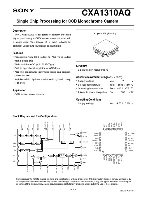
CXA1310AQ中文资料
–1–
E89Z21A78-PS
元器件交易网
CXA1310AQ
Pin Description No. Symbol
I/O signal
Equivalent circuit
Description
1 SAG
2 GND2 3 GND1
4 SYNC
Inputs VIDEO OUT through capacitor
21 150Ω
100µA
Input pin of the sample / hold pulse (active at High)
[∗1]
[∗2]
22
22 DATA
[∗1] MAX 800mV [∗2] MAX 800mV
150µA
CCD signal input pin ∗ External applied voltage
White clip level adjusting pin
6 WC CONT GND∗ 2 to 3.5V∗
6 150Ω
Preset mode
40µA
Control mode ∗ External applied voltage
–2–
元器件交易网
No. Symbol
I/O signal
–5–
元器件交易网
CXA1310AQ
No. Symbol
I/O signal
Equivalent circuit
Description
23 PG
[∗1]
[∗2]
23
[∗1] MAX 800mV [∗2] MAX 800mV
150µA
CCD single input pin
- 1、下载文档前请自行甄别文档内容的完整性,平台不提供额外的编辑、内容补充、找答案等附加服务。
- 2、"仅部分预览"的文档,不可在线预览部分如存在完整性等问题,可反馈申请退款(可完整预览的文档不适用该条件!)。
- 3、如文档侵犯您的权益,请联系客服反馈,我们会尽快为您处理(人工客服工作时间:9:00-18:30)。
Series H - Power Entry Modules
2
6
Faston, Straight 55.90 30.20 20.60 40.01 —
— CCM1607-ND
16.41 287.00
958.00
Series P, Chameleon — For General or Medical Applications (See chart for part number break down)
元器件交易网
Power Entry Modules (Cont.)
Rated Current Fig. 120V (Amps)
Termination
Dimensions (mm)
Digi-Key
A
B
C
D
E
F Part No.
Pricing
1
25
100
Series EJS — Enhanced Performance Snap-In Compact RFI Filter IEC Connector Package
EDP Series: These RFI power line filters provide enhanced differential-mode performance for applications requiring more line-to-line protection.
EJT Series: The EJT Series is a power inlet filter designed to attenuate noise up to 1 GHz. This inlet uses an IEC 320/C14 input connector. This product was designed to address the demand for more noise attenuation at higher frequencies in a compact inlet.
10A
6
10
10
6
6
6
Faston Faston Faston Faston Faston Faston
31.50 54.10 58.67 26.92 55.91 — CCM1378-ND 31.50 54.10 58.67 28.50 55.91 — CCM1379-ND 31.50 54.10 58.67 28.50 55.91 — CCM1380-ND 31.50 54.10 58.67 26.92 55.91 — CCM1381-ND 31.50 54.10 58.67 28.50 55.91 — CCM1382-ND 31.50 54.10 58.67 26.92 55.91 — CCM1600-ND
1
3
8
6
10
15
Straight Straight Straight Straight Straight
55.88 27.94 24.38 30.10 34.21 — CCM1252-ND 55.88 27.94 24.38 30.10 34.21 — CCM1253-ND 55.88 27.94 24.38 30.10 34.21 — CCM1254-ND 55.88 27.94 24.38 30.10 34.21 — CCM1255-ND 55.88 27.94 24.38 30.10 34.21 — CCM1256-ND
50.22 40.01 22.76 31.09
CCM1401-ND
30.40 — 22.66 30.61
CCM1402-ND
35.31 — 28.19 35.71
CCM1403-ND
50.01 40.01 29.31 35.71
CCM1404-ND
Pricing
1
25
100
3.23 56.50 189.00 2.35 41.00 137.00 2.47 43.00 144.00 2.86 50.00 167.00 2.86 50.00 167.00
1
16.17 28.90
54.62
20.92 24.40 24.40 31.02 30.50 33.99 30.11 26.14
4.82
Pricing
Corcom
25
100
Part No.
282.50 505.25
955.00
365.75 426.50 426.50 542.25 533.25 594.25 526.25 457.00
Rated Current 120V Fig. (Amps)
RFI Filter Type
Available
Voltage DPSTSel Nhomakorabeaction On/Off
Position Switch
A
Dimensions (mm)
B
C
DE
Digi-Key Part No.
Series J — Power Entry Modules
* Unfiltered † Utilizes 2 5x20 fuses
17.43 23.58 26.45 24.94
304.75 412.25 462.25 436.00
1018.00 1377.00 1544.00 1457.00
Corcom Part No.
1EJS1 3EJS1 6EJS1 10EJS1 15EJS1 20EJS1
6EH4
PS0SXS000 PS000S000 PS0S0SBX0 PS000SS3B PS0SXSS30 PS0SXSS60 PS0S0SSXA PS000SSXB PS0SXDS60 PS0S0SS6A PS0S0SS60 PE0SSS000 PE0SSSS60 PE0SSSSX0 PE0S0SS30
6
Unfiltered
4
11
6
Gen. Purpose
4
—
68.07 38.61 29.72 31.24 — CCM1200-ND
—
69.85 47.50 29.73 40.13 — CCM1201-ND
Series LA — Power Entry Modules
12
5
Gen. Purpose
2
—
EOP Series: A general purpose filter which is effective in removing both common and differential-mode noise for susceptibility applications.
EP Series: The EP/VP series of RFI filters has been developed to reduce conducted noise to acceptable limits for equipment that must comply with requirements of CISPAR in Europe and the FCC specifications in the USA.
Corcom Part No.
6ESRM-P 6ESRM-3 6ESRMC2 6ESRFC3 6ESRF-3
220-240
Fig. 11
C
D B
Fig. 12 A B
C
220-240
Fig. 13
A
DVE
D
C
D B A
Note: Picture shown with switch. Fig. 14
E
10
Faston
31.50 49.02 58.67 26.92 55.91 — CCM1372-ND*
16.38 286.25
956.00
10
Faston
31.50 49.02 58.67 26.92 55.91 — CCM1373-ND*
12.77 223.50
746.00
10
Faston
31.50 54.10 58.67 26.92 55.91 — CCM1374-ND
10B
D
6 10 3
Faston Faston Faston
50.29 50.29 50.29
54.10 54.10 54.10
58.67 58.67 58.67
28.50 28.50 28.50
55.91 55.91 55.91
40.01 40.01 40.01
CCM1383-ND CCM1384-ND CCM1385-ND
19.53 341.50 1141.00
3
Faston
31.50 54.10 58.67 28.50 55.91 — CCM1376-ND
24.35 425.50 1422.00
3
Faston
31.50 54.10 58.67 26.92 55.91 — CCM1377-ND
23.89 417.75 1395.00
MA604
Rated Current 125V Fig. (Amps)
15
15
15
15
15
15
Output Terminals
Mounting Input Style Config.
PC Terminals Quick Disconnect Quick Disconnect Quick Disconnect Quick Disconnect
Flange Flange Snap-In Snap-In Flange
Male Male Male Female Female
Dimensions (mm)