Electrokinetic and magnetic fields generated by flow through a fractured zone a sensitivity
磁共振(磁谐振耦合)无线充电技术鼻祖级文章-英文原文
Wireless Power Transfer via Strongly Coupled Magnetic ResonancesAndré Kurs,1* Aristeidis Karalis,2 Robert Moffatt,1 J. D. Joannopoulos,1 Peter Fisher,3Marin Soljačić11Department of Physics, Massachusetts Institute of Technology, Cambridge, MA 02139, USA. 2Department of Electrical Engineering and Computer Science, Massachusetts Institute of Technology, Cambridge, MA 02139, USA. 3Department of Physics and Laboratory for Nuclear Science, Massachusetts Institute of Technology, Cambridge, MA 02139, USA.*To whom correspondence should be addressed. E-mail: akurs@Using self-resonant coils in a strongly coupled regime, we experimentally demonstrate efficient non-radiative power transfer over distances of up to eight times the radius of the coils. We demonstrate the ability to transfer 60W with approximately 40% efficiency over distances in excess of two meters. We present a quantitative model describing the power transfer which matches the experimental results to within 5%. We discuss practical applicability and suggest directions for further studies. At first glance, such power transfer is reminiscent of the usual magnetic induction (10); however, note that the usual non- resonant induction is very inefficient for mid-range applications.Overview of the formalism. Efficient mid-range power transfer occurs in particular regions of the parameter space describing resonant objects strongly coupled to one another. Using coupled-mode theory to describe this physical system (11), we obtain the following set of linear equationsIn the early 20th century, before the electrical-wire grid, Nikola Tesla (1) devoted much effort towards schemes to a&m(t)=(iωm-Γm)a m(t)+∑iκmn a n(t)+F m(t)n≠m(1)transport power wirelessly. However, typical embodiments (e.g. Tesla coils) involved undesirably large electric fields. During the past decade, society has witnessed a dramatic surge of use of autonomous electronic devices (laptops, cell- phones, robots, PDAs, etc.) As a consequence, interest in wireless power has re-emerged (2–4). Radiative transfer (5), while perfectly suitable for transferring information, poses a number of difficulties for power transfer applications: the efficiency of power transfer is very low if the radiation is omnidirectional, and requires an uninterrupted line of sight and sophisticated tracking mechanisms if radiation is unidirectional. A recent theoretical paper (6) presented a detailed analysis of the feasibility of using resonant objects coupled through the tails of their non-radiative fields for mid- range energy transfer (7). Intuitively, two resonant objects of the same resonant frequency tend to exchange energy efficiently, while interacting weakly with extraneous off- resonant objects. In systems of coupled resonances (e.g. acoustic, electro-magnetic, magnetic, nuclear, etc.), there is often a general “strongly coupled” regime of operation (8). If one can operate in that regime in a given system, the energy transfer is expected to be very efficient. Mid-range power transfer implemented this way can be nearly omnidirectional and efficient, irrespective of the geometry of the surrounding space, and with low interference and losses into environmental objects (6).Considerations above apply irrespective of the physical nature of the resonances. In the current work, we focus on one particular physical embodiment: magnetic resonances (9). Magnetic resonances are particularly suitable for everyday applications because most of the common materials do not interact with magnetic fields, so interactions with environmental objects are suppressed even further. We were able to identify the strongly coupled regime in the system of two coupled magnetic resonances, by exploring non-radiative (near-field) magnetic resonant induction at MHzfrequencies. where the indices denote the different resonant objects. The variables a m(t) are defined so that the energy contained in object m is |a m(t)|2, ωm is the resonant frequency of thatisolated object, and Γm is its intrinsic decay rate (e.g. due to absorption and radiated losses), so that in this framework anuncoupled and undriven oscillator with parameters ω0 and Γ0 would evolve in time as exp(iω0t –Γ0t). The κmn= κnm are coupling coefficients between the resonant objects indicated by the subscripts, and F m(t) are driving terms.We limit the treatment to the case of two objects, denoted by source and device, such that the source (identified by the subscript S) is driven externally at a constant frequency, and the two objects have a coupling coefficient κ. Work is extracted from the device (subscript D) by means of a load (subscript W) which acts as a circuit resistance connected to the device, and has the effect of contributing an additional term ΓW to the unloaded device object's decay rate ΓD. The overall decay rate at the device is therefore Γ'D= ΓD+ ΓW. The work extracted is determined by the power dissipated in the load, i.e. 2ΓW|a D(t)|2. Maximizing the efficiency η of the transfer with respect to the loading ΓW, given Eq. 1, is equivalent to solving an impedance matching problem. One finds that the scheme works best when the source and the device are resonant, in which case the efficiency isThe efficiency is maximized when ΓW/ΓD= (1 + κ2/ΓSΓD)1/2. It is easy to show that the key to efficient energy transfer is to have κ2/ΓSΓD> 1. This is commonly referred to as the strongcoupling regime. Resonance plays an essential role in thisDS S D'' power transfer mechanism, as the efficiency is improved by approximately ω2/ΓD 2 (~106 for typical parameters) compared to the case of inductively coupled non-resonant objects. Theoretical model for self-resonant coils. Ourexperimental realization of the scheme consists of two self- resonant coils, one of which (the source coil) is coupled inductively to an oscillating circuit, while the other (the device coil) is coupled inductively to a resistive load (12) (Fig. 1). Self-resonant coils rely on the interplay between distributed inductance and distributed capacitance to achieve resonance. The coils are made of an electrically conducting wire of total length l and cross-sectional radius a wound into Given this relation and the equation of continuity, one finds that the resonant frequency is f 0 = 1/2π[(LC )1/2]. We can now treat this coil as a standard oscillator in coupled-mode theory by defining a (t ) = [(L /2)1/2]I 0(t ).We can estimate the power dissipated by noting that the sinusoidal profile of the current distribution implies that the spatial average of the peak current-squared is |I 0|2/2. For a coil with n turns and made of a material with conductivity σ, we modify the standard formulas for ohmic (R o ) and radiation (R r ) µ0ω l a helix of n turns, radius r , and height h . To the best of our knowledge, there is no exact solution for a finite helix in the literature, and even in the case of infinitely long coils, the solutions rely on assumptions that are inadequate for our R o = 2σ 4πa µ πωr 42 ωh 2 (6)system (13). We have found, however, that the simple quasi- R =0 n 2 + (7)static model described below is in good agreementr ε 12 c3π3 c(approximately 5%) with experiment.We start by observing that the current has to be zero at the ends of the coil, and make the educated guess that the resonant modes of the coil are well approximated bysinusoidal current profiles along the length of the conducting wire. We are interested in the lowest mode, so if we denote by s the parameterization coordinate along the length of the conductor, such that it runs from -l /2 to +l /2, then the time- dependent current profile has the form I 0 cos(πs /l ) exp(i ωt ). It follows from the continuity equation for charge that the linear charge density profile is of the form λ0 sin(πs /l ) exp(i ωt ), so the two halves of the coil (when sliced perpendicularly to its axis) contain charges equal in magnitude q 0 = λ0l /π but opposite in sign.As the coil is resonant, the current and charge density profiles are π/2 out of phase from each other, meaning that the real part of one is maximum when the real part of the other is zero. Equivalently, the energy contained in the coil is 0The first term in Eq. 7 is a magnetic dipole radiation term(assuming r << 2πc /ω); the second term is due to the electric dipole of the coil, and is smaller than the first term for our experimental parameters. The coupled-mode theory decay constant for the coil is therefore Γ = (R o + R r )/2L , and its quality factor is Q = ω/2Γ.We find the coupling coefficient κDS by looking at the power transferred from the source to the device coil,assuming a steady-state solution in which currents and charge densities vary in time as exp(i ωt ).P =⎰d rE (r )⋅J (r ) =-⎰d r (A&S (r )+∇φS (r ))⋅J D (r ) at certain points in time completely due to the current, and at other points, completely due to the charge. Usingelectromagnetic theory, we can define an effective inductance L and an effective capacitance C for each coil as follows:=-1⎰⎰d r d r ' µJ &S(r ')+ρS(r ') 4π |r -r |ε0≡-i ωMI S I Dr '-r|r '-r |3⋅J D (r )(8)L =µ04π |I 0 |⎰⎰d r d r 'J (r )⋅J (r ')|r -r '|where the subscript S indicates that the electric field is due to the source. We then conclude from standard coupled-mode theory arguments that κDS = κSD = κ = ωM /2[(L S L D )1/2]. When 1 1 ρ(r )ρ(r ') the distance D between the centers of the coils is much larger= C 4πε 0 |q 0 | ⎰⎰d r d r ' |r -r '|(4)than their characteristic size, κ scales with the D -3dependence characteristic of dipole-dipole coupling. Both κ and Γ are functions of the frequency, and κ/Γ and the where the spatial current J (r ) and charge density ρ(r ) are obtained respectively from the current and charge densities along the isolated coil, in conjunction with the geometry of the object. As defined, L and C have the property that the efficiency are maximized for a particular value of f , which is in the range 1-50MHz for typical parameters of interest. Thus, picking an appropriate frequency for a given coil size, as we do in this experimental demonstration, plays a major role in optimizing the power transfer.1 2Comparison with experimentallydeterminedU =2 L |I 0 |parameters. The parameters for the two identical helical coils built for the experimental validation of the power 1 2 transfer scheme are h = 20cm, a = 3mm, r = 30 cm, and n = =2C|q 0 | (5)5.25. Both coils are made of copper. The spacing between loops of the helix is not uniform, and we encapsulate theuncertainty about their uniformity by attributing a 10% (2cm) uncertainty to h . The expected resonant frequency given these22dimensions is f0 = 10.56 ± 0.3MHz, which is about 5% off from the measured resonance at 9.90MHz.The theoretical Q for the loops is estimated to be approximately 2500 (assuming σ = 5.9 × 10⁷ m/Ω) but the measured value is Q = 950±50. We believe the discrepancy is mostly due to the effect of the layer of poorly conductingcopper oxide on the surface of the copper wire, to which the current is confined by the short skin depth (~20μm) at this frequency. We therefore use the experimentally observed Q and ΓS= ΓD= Γ = ω/2Q derived from it in all subsequent computations.We find the coupling coefficient κ experimentally by placing the two self-resonant coils (fine-tuned, by slightly adjusting h, to the same resonant frequency when isolated) a distance D apart and measuring the splitting in the frequencies of the two resonant modes. According to coupled-mode theory, this splitting should be ∆ω = 2[(κ2-Γ2)1/2]. In the present work, we focus on the case where the two coils are aligned coaxially (Fig. 2), although similar results are obtained for other orientations (figs. S1 and S2).Measurement of the efficiency. The maximum theoretical efficiency depends only on the parameter κ/[(L S L D)1/2] = κ/Γ, which is greater than 1 even for D = 2.4m (eight times the radius of the coils) (Fig. 3), thus we operate in the strongly- coupled regime throughout the entire range of distances probed.As our driving circuit, we use a standard Colpitts oscillator whose inductive element consists of a single loop of copper wire 25cm in radius(Fig. 1); this loop of wire couples inductively to the source coil and drives the entire wireless power transfer apparatus. The load consists of a calibrated light-bulb (14), and is attached to its own loop of insulated wire, which is placed in proximity of the device coil and inductively coupled to it. By varying the distance between the light-bulb and the device coil, we are able to adjust the parameter ΓW/Γ so that it matches its optimal value, given theoretically by (1 + κ2/Γ2)1/2. (The loop connected to the light-bulb adds a small reactive component to ΓW which is compensated for by slightly retuning the coil.) We measure the work extracted by adjusting the power going into the Colpitts oscillator until the light-bulb at the load glows at its full nominal brightness.We determine the efficiency of the transfer taking place between the source coil and the load by measuring the current at the mid-point of each of the self-resonant coils with a current-probe (which does not lower the Q of the coils noticeably.) This gives a measurement of the current parameters I S and I D used in our theoretical model. We then compute the power dissipated in each coil from P S,D=ΓL|I S,D|2, and obtain the efficiency from η = P W/(P S+ P D+P W). To ensure that the experimental setup is well described by a two-object coupled-mode theory model, we position the device coil such that its direct coupling to the copper loop attached to the Colpitts oscillator is zero. The experimental results are shown in Fig. 4, along with the theoretical prediction for maximum efficiency, given by Eq. 2. We are able to transfer significant amounts of power using this setup, fully lighting up a 60W light-bulb from distances more than 2m away (figs. S3 and S4).As a cross-check, we also measure the total power going from the wall power outlet into the driving circuit. The efficiency of the wireless transfer itself is hard to estimate in this way, however, as the efficiency of the Colpitts oscillator itself is not precisely known, although it is expected to be far from 100% (15). Still, the ratio of power extracted to power entering the driving circuit gives a lower bound on the efficiency. When transferring 60W to the load over a distance of 2m, for example, the power flowing into the driving circuit is 400W. This yields an overall wall-to-load efficiency of 15%, which is reasonable given the expected efficiency of roughly 40% for the wireless power transfer at that distance and the low efficiency of the Colpitts oscillator.Concluding remarks. It is essential that the coils be on resonance for the power transfer to be practical (6). We find experimentally that the power transmitted to the load drops sharply as either one of the coils is detuned from resonance. For a fractional detuning ∆f/f0 of a few times the inverse loaded Q, the induced current in the device coil is indistinguishable from noise.A detailed and quantitative analysis of the effect of external objects on our scheme is beyond the scope of the current work, but we would like to note here that the power transfer is not visibly affected as humans and various everyday objects, such as metals, wood, and electronic devices large and small, are placed between the two coils, even in cases where they completely obstruct the line of sight between source and device (figs. S3 to S5). External objects have a noticeable effect only when they are within a few centimeters from either one of the coils. While some materials (such as aluminum foil, styrofoam and humans) mostly just shift the resonant frequency, which can in principle be easily corrected with a feedback circuit, others (cardboard, wood, and PVC) lower Q when placed closer than a few centimeters from the coil, thereby lowering the efficiency of the transfer.When transferring 60W across 2m, we calculate that at the point halfway between the coils the RMS magnitude of the electric field is E rms= 210V/m, that of the magnetic field isH rms= 1A/m, and that of the Poynting vector is S rms=3.2mW/cm2 (16). These values increase closer to the coils, where the fields at source and device are comparable. For example, at distances 20cm away from the surface of the device coil, we calculate the maximum values for the fields to be E rms= 1.4kV/m, H rms= 8A/m, and S rms= 0.2W/cm2. The power radiated for these parameters is approximately 5W, which is roughly an order of magnitude higher than cell phones. In the particular geometry studied in this article, the overwhelming contribution (by one to two orders of magnitude) to the electric near-field, and hence to the near- field Poynting vector, comes from the electric dipole moment of the coils. If instead one uses capacitively-loaded single- turn loop design (6) - which has the advantage of confining nearly all of the electric field inside the capacitor - and tailors the system to operate at lower frequencies, our calculations show (17) that it should be possible to reduce the values cited above for the electric field, the Poynting vector, and the power radiated to below general safety regulations (e.g. the IEEE safety standards for general public exposure(18).) Although the two coils are currently of identical dimensions, it is possible to make the device coil small enough to fit into portable devices without decreasing the efficiency. One could, for instance, maintain the product of the characteristic sizes of the source and device coils constant, as argued in (6).We believe that the efficiency of the scheme and the power transfer distances could be appreciably improved by silver-plating the coils, which should increase their Q, or by working with more elaborate geometries for the resonant objects (19). Nevertheless, the performance characteristics of the system presented here are already at levels where they could be useful in practical applications.References and Notes1. N. Tesla, U.S. patent 1,119,732 (1914).2.J. M. Fernandez, J. A. Borras, U.S. patent 6,184,651(2001).3.A. Esser, H.-C. Skudelny, IEEE Trans. Indust. Appl. 27,872(1991).4.J. Hirai, T.-W. Kim, A. Kawamura, IEEE Trans. PowerElectron. 15, 21(2000).5.T. A. Vanderelli, J. G. Shearer, J. R. Shearer, U.S. patent7,027,311(2006).6.A. Karalis, J. D. Joannopoul os, M. Soljačić, Ann. Phys.,10.1016/j.aop.2007.04.017(2007).7.Here, by mid-range, we mean that the sizes of the deviceswhich participate in the power transfer are at least a few times smaller than the distance between the devices. For example, if the device being powered is a laptop (size ~ 50cm), while the power source (size ~ 50cm) is in thesame room as the laptop, the distance of power transfer could be within a room or a factory pavilion (size of the order of a fewmeters).8. T. Aoki, et al., Nature 443, 671 (2006).9.K. O’Brien, G. Scheible, H. Gueldner, 29th AnnualConference of the IEEE 1, 367(2003).10.L. Ka-Lai, J. W. Hay, P. G. W., U.S. patent7,042,196(2006).11.H. Haus, Waves and Fields in Optoelectronics(Prentice- Supporting Online Material/cgi/content/full/1143254/DC1SOM TextFigs. S1 to S530 March 2007; accepted 21 May 2007Published online 7 June 2007; 10.1126/science.1143254 Include this information when citing this paper.Fig. 1. Schematic of the experimental setup. A is a single copper loop of radius 25cm that is part of the driving circuit, which outputs a sine wave with frequency 9.9MHz. S and D are respectively the source and device coils referred to in the text. B is a loop of wire attached to the load (“light-bulb”). The various κ’s represent direct couplings between the objects indicated by the arrows. The angle between coil D and the loop A is adjusted to ensure that their direct coupling is zero, while coils S and D are aligned coaxially. The direct couplings between B and A and between B and S are negligible.Fig. 2. Comparison of experimental and theoretical values for κ as a function of the separation between coaxially aligned source and device coils (the wireless power transfer distance.) Fig. 3. Comparison of experimental and theoretical values for the parameter κ/Γ as a function of the wireless power transfer distance. The theory values are obtained by using the theoretical κ and the experimentally measured Γ. The shaded area represents the spread in the theoretical κ/Γ due to the 5% uncertainty in Q.Fig. 4. Comparison of experimental and theoretical efficiencies as functions of the wireless power transfer distance. The shaded area represents the theoretical prediction for maximum efficiency, and is obtained by inserting theHall, Englewood Cliffs, NJ, 1984).12.The couplings to the driving circuit and the load donot theoretical values from Fig. 3 into Eq. 2 [with Γκ2/Γ2 1/2 W /ΓD= (1 +have to be inductive. They may also be connected by awire, for example. We have chosen inductive coupling in the present work because of its easier implementation. 13.S. Sensiper, thesis, Massachusetts Institute of Technology(1951).14.We experimented with various power ratings from 5W to75W.15.W. A. Edson, Vacuum-Tube Oscillators (Wiley, NewYork,1953).16.Note that E ≠cμ0H, and that the fields are out of phaseand not necessarily perpendicular because we are not in a radiativeregime.17.See supporting material on Science Online.18.IEEE Std C95.1—2005 IEEE Standard for Safety Levelswith Respect to Human Exposure to Radio FrequencyElectromagnetic Fields, 3 kHz to 300 GHz (IEEE,Piscataway, NJ,2006).19. J. B. Pendry, Science 306, 1353 (2004).20. The authors would like to thank John Pendry forsuggesting the use of magnetic resonances, and Michael Grossman and Ivan Čelanović for technical assistance.This work was supported in part by the Materials Research Science and Engineering Center program of the National Science Foundation under Grant No. DMR 02-13282, by the U.S. Department of Energy under Grant No. DE-FG02-99ER45778, and by the Army Research Officethrough the Institute for Soldier Nanotechnologies under Contract No. DAAD-19-02-D0002.) ]. The black dots are the maximum efficiency obtained from Eq. 2 and the experimental values of κ/Γ from Fig. 3. The red dots present the directly measured efficiency,as described in thetext.。
Lecture 1 磁性物理和磁学基本概念
Topics for your report:
Recent progress in advanced -
1. Nanocomposite Rare-earth permanent magnetic materials;
2. Nanocomposite soft magnetic materials; 3. perpendicular magnetic recording; 4. Magnetoelectric materials; 5. Magnetic thin films for microwave absorber; 6. GMR materials; 7. One-dimension magnetic nanostructures;
Pliny the Elder (23-79 AD Roman) wrote of a hill near the river Indus that was made entirely of a stone that attracted iron.
Known in China and Europe 800 BC
When lightning strikes the earth it could create a magnetic field large enough to saturate the magnetization of lodestone .
Once ቤተ መጻሕፍቲ ባይዱn 1 – 10 million years
磁性材料:原理、工艺与应用
Magnetic Materials: Basic theory, Processing and Applications
Lecture 1 磁学基本概念与磁性物理基础
TEM,TE AND TM MODES FOR WAVEGUIDES,RECTANGULAR WAVEGUIDE
Whites, EE 481 Lecture 10 Page 1 of 10© 2011 Keith W. WhitesLecture 10: TEM, TE, and TM Modes for Waveguides. Rectangular Waveguide.We will now generalize our discussion of transmission lines by considering EM waveguides . These are “pipes” that guide EM waves. Coaxial cables, hollow metal pipes, and fiber optical cables are all examples of waveguides.We will assume that the waveguide is invariant in the z -direction:z and that the wave is propagating in z as j z e β−. (We could alsohave assumed propagation in –z .)Types of EM WavesWe will first develop an extremely interesting property of EM waves that propagate in homogeneous waveguides. This will lead to the concept of “modes ” and their classification as• Transverse Electric and Magnetic (TEM),•Transverse Electric (TE), or • Transverse Magnetic (TM).Proceeding from the Maxwell curl equations: ˆˆˆx y zx y zE j H j H xy z E E E ωμωμ∂∂∂∇×=−⇒=−∂∂∂ or ˆx : y z x E E j H y zωμ∂∂−=−∂∂ ˆy : x z y E E j H xz ωμ∂∂⎛⎞−−=−⎜⎟∂∂⎝⎠ ˆz : y x z E E j H x yωμ∂∂−=−∂∂However, the spatial variation in z is known so that()()j z j z e j e zβββ−−∂=−∂ Consequently, these curl equations simplify to z y x E j E j H yβωμ∂+=−∂ (3.3a),(1) z x y E j E j H xβωμ∂−−=−∂ (3.3b),(2) y x z E E j H x yωμ∂∂−=−∂∂ (3.3c),(3)We can perform a similar expansion of Ampère’s equation H j E ωε∇×= to obtain z y x H j H j E yβωε∂+=∂ (3.4a),(4) z x y H j H j E xβωε∂−−=∂ (3.4b),(5) y x z H H j E x yωε∂∂−=∂∂ (3.5c),(6)Now, (1)-(6) can be manipulated to produce simple algebraic equations for the transverse (x and y ) components of E and H . For example, from (1): z x y j E H j E y βωμ⎛⎞∂=+⎜⎟∂⎝⎠Substituting for E y from (5) we find 2221z z x x z z x j E H H j j H y j x j E j H H y xββωμωεββωμωμεωμε⎡⎤∂∂⎛⎞=+−−⎜⎟⎢⎥∂∂⎝⎠⎣⎦∂∂=+−∂∂ or,where 222c k k β≡− and 22k ωμε=. (3.6)Similarly, we can show thatMost important point: From (7)-(10), we can see that all transverse components of E and H can be determined from only the axial components z E and z H . It is this fact that allows the mode designations TEM, TE, and TM.Furthermore, we can use superposition to reduce the complexity of the solution by considering each of these mode types separately, then adding the fields together at the end.TE Modes and Rectangular WaveguidesA transverse electric (TE) wave has 0z E = and 0z H ≠. Consequently, all E components are transverse to the direction of propagation. Hence, in (7)-(10) with 0z E =, then all transverse components of E and H are known once we find a solution for only z H . Neat!For a rectangular waveguide , the solutions for x E , y E , x H , y H , and z H are obtained in Section 3.3 of the text. The solution and the solution process are interesting, but not needed in this course.Therefore,These m and n indices indicate that only discrete solutions for the transverse wavenumber (k c ) are allowed. Physically, this occurs because we’ve bounded the system in the x and y directions. (A vaguely similar situation occurs in atoms, leading to shell orbitals.)Notice something important. From (11), we find that 0m n == means that ,000c k =. In (7)-(10), this implies infinite field amplitudes, which is not a physical result. Consequently, the 0m n == TE or TM modes are not allowed.One exception might occur if 0z z E H == since this leads to indeterminate forms in (7)-(10). However, it can be shown that inside hollow metallic waveguides when both 0m n == and0z z E H ==, then 0E H ==. This means there is no TEM mode.Consequently, EM waves will propagate only when the frequency is “large enough ” since there is no TEM mode. Otherwise β will be imaginary (j βα→−), leading to pure attenuation and no propagation of the wave j z z e e βα−−→.This turns out to be a general result. That is, for a hollow conductor, EM waves will propagate only when the frequency is large enough and exceeds some lower threshold. This minimum propagation frequency is called the cutoff frequency ,c mn f.It can be shown that guided EM waves require at least two distinct conductors in order to support wave propagation all the way down to 0+ Hz.The cutoff frequencies for TE modes in a rectangular waveguide are determined from (12) with 0β= to be,,0,1,(0)c mn m n f m n ===≠… (3.84),(13) In other words, these are the frequencies where 0mn β= and wave propagation begins when the frequency slightly exceeds ,c mn f .For an X-band rectangular waveguide, the cross-sectional dimensions are a = 2.286 cm and b = 1.016 cm. Using (13):TE m,n Mode Cutoff Frequenciesm n f c,mn(GHz)1 0 6.5622 0 13.1230 1 14.7641 1 16.156In the X-band region (≈ 8.2-12.5 GHz), only the TE10 mode can propagate in the waveguide regardless of how it is excited. (We’ll also see shortly that no TM modes will propagate either.) This is called single mode operation and is most often the preferred application for hollow waveguides.On the other hand, at 15.5 GHz any combination of the first three of these modes could exist and propagate inside a metal, rectangular waveguide. Which combination actually exists will depend on how the waveguide is excited.Note that the TE11 mode (and all higher-ordered TE modes) could not propagate. (We’ll also see next that no TM modes will propagate at 15.5 GHz either.)TM Modes and Rectangular WaveguidesConversely to TE modes, transverse magnetic (TM) modes have 0z H = and 0z E ≠.The expression for the cutoff frequencies of TM modes in a rectangular waveguide,,1,2c mn f m n ==… (14) is very similar to that for TE modes given in (13).It can be shown that if either 0m = or 0n = for TM modes, then 0E H ==. This means that no TM modes with 0m = or 0n = are allowable in a rectangular waveguide.For an X-band waveguide:TM m ,n Mode Cutoff Frequencies m n f c ,mn (GHz)1 1 16.1561 2 30.2482 1 19.753Therefore, no TM modes can propagate in an X-band rectangular waveguide when f < 16.156 GHz.Dominant ModeNote that from 6.56 GHz f ≤≤ 13.12 GHz in the X-band rectangular waveguide, only the TE 10 mode can propagate. This mode is called the dominant mode of the waveguide.See Fig 3.9 in the text for plots of the electric and magnetic fields associated with this mode.TEM ModeThe transverse electric and magnetic (TEM) modes are characterized by 0z E = and 0z H =.In order for this to occur, it can be shown from (3.4) and (3.5) that it is necessary for 0c f =. In other words, there is no cutoff frequency for waveguides that support TEM waves.Rectangular, circular, elliptical, and all hollow, metallic waveguides cannot support TEM waves.It can be shown that at least two separate conductors are required for TEM waves. Examples of waveguides that willallow TEM modes include coaxial cable, parallel plate waveguide, stripline, and microstrip.Microstrip is the type of microwave circuit interconnection that we will use in this course. This “waveguide” will support the “quasi-TEM” mode, which like regular TEM modes has no non-zero cutoff frequency.However, if the frequency is large enough, other modes will begin to propagate on a microstrip. This is usually not a desirable situation.。
文献翻译(二次电流层)
激光等离子体相互作用中磁重联引起的等离子体与二次电流层生成的研究摘要:以尼尔逊[物理学家、列托人,97,255001,(2006)]为代表的科学家首次对等离子体相互作用引起的磁重联进行了研究,该研究在固体等离子体层上进行,在两个激光脉冲中间设置一定间隔,在两个激光斑点之间可以发现一条细长的电流层(CS),为了更加贴切的模拟磁重联过程,我们应该设置两个并列的目标薄层。
实验过程中发现,细长的电流层的一端出现一个折叠的电子流出区域,该区域中含有三条平行的电子喷射线,电子射线末端能量分布符合幂律法则。
电子主导磁重联区域强烈的感应电场增强了电子加速,当感应电场处于快速移动的等离子体状态时还会进一步加速,另外弹射过程会引起一个二级电流层。
正文:等离子体的磁重联与爆炸过程磁能量进入等离子体动能和热能能量的相互转换有关。
发生磁重联的薄层区域加速并释放等离子体[1-5]。
实验中磁重联速度与太阳能的观察结果大于Sweet-Parker与相关模型[4-6]的标准值,这是由霍尔电流和湍流[7-12]引起的。
二级磁岛以及该区域释放的等离子体可以提高磁重联速度,当伦德奎斯特数S﹥104[13]时二级磁导很不稳定。
这些理论预测值与近地磁尾离子扩散区域中心附近的二级磁岛观察值相符[14],激光束与物质的相互作用的过程中,正压机制激发兆高斯磁场(▽ne×▽Te)生成[15-16]。
以尼尔逊[17]为代表的科学家首次运用两个类似的的激光产生的等离子体模拟磁重联过程。
尼尔逊[17]与Li[18]等人实验测量数据为磁重联的存在提供了决定性的证据,他们运用了随时间推移的质子偏转技术来研究磁拓扑变化,除此之外尼尔逊[17]等人观察到高度平行双向等离子喷射线与预期的磁重联平面成40°夹角。
本次研究调查了自发磁场的无碰撞重联,激光等离子体相互作用产生等离子体,为了防止磁场与等离子体连接在一起实验过程使用了两个共面有一定间隔的等离子体。
微纳米流动和核磁共振技术
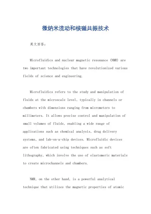
微纳米流动和核磁共振技术英文回答:Microfluidics and nuclear magnetic resonance (NMR) are two important technologies that have revolutionized various fields of science and engineering.Microfluidics refers to the study and manipulation of fluids at the microscale level, typically in channels or chambers with dimensions ranging from micrometers to millimeters. It allows precise control and manipulation of small volumes of fluids, enabling a wide range of applications such as chemical analysis, drug delivery systems, and lab-on-a-chip devices. Microfluidic devices are often fabricated using techniques such as soft lithography, which involve the use of elastomeric materials to create microchannels and chambers.NMR, on the other hand, is a powerful analytical technique that utilizes the magnetic properties of atomicnuclei to study the structure and dynamics of molecules. It is based on the principle of nuclear spin, which is the intrinsic angular momentum possessed by atomic nuclei. By subjecting a sample to a strong magnetic field and applying radiofrequency pulses, NMR can provide information about the chemical composition, molecular structure, and molecular interactions of the sample. NMR has diverse applications in fields such as chemistry, biochemistry, medicine, and materials science.Microfluidics and NMR can be combined to create powerful analytical tools for studying various biological and chemical systems. For example, microfluidic devices can be used to precisely control the flow of samples and reagents, while NMR can provide detailed information about the composition and structure of the samples. This combination has been used in the development ofmicrofluidic NMR systems, which allow rapid and sensitive analysis of small sample volumes. These systems have been applied in areas such as metabolomics, drug discovery, and environmental monitoring.中文回答:微纳米流体力学和核磁共振技术是两种重要的技术,已经在科学和工程的各个领域引起了革命性的变化。
Magnetism and magnetic properties of materials

Magnetism and magnetic properties ofmaterials介绍磁性及其磁性能是材料科学中很重要的一块,磁性是指物质受到磁场作用时表现出来的各种现象,如吸引或排斥等。
而磁性能是指物质在磁场中的一系列特性表现。
磁性不仅影响着我们生活中常用的许多物品,如电视、电脑、磁性材料,而且还对应用在电磁设备、航空航天、生物医学等方面具有重要的应用价值。
磁性基础知识磁性是由原子和分子的磁性质决定的。
原子既具有电子轨道运动所形成的轨道磁矩,又具有自旋运动所形成的自旋磁矩。
物质的磁性取决于自旋磁矩、轨道磁矩的合成,并受到分子结构、晶格结构、温度等因素的影响。
然而,对于许多材料而言,这种合成是非常微弱的,因此物质磁化的来源主要是出现了局域磁时原子间作用的形成及相互偏转。
物质磁化度的计量单位是磁通量密度,即每个单位面积上磁通量的总数。
如果表面积为A, 磁通量为Φ,磁化密度J可以用下式表示:J = Φ/A磁性种类物质的磁性取决于其内部的微观结构,不同结构具有不同的磁性。
根据物质的磁特性,可分为顺磁性、铁磁性、反磁性及亚铁磁性。
顺磁性是指物质受磁场作用后,始终在磁场的方向上产生一个磁矩,而它的方向又是与磁场方向相同的微弱磁性。
顺磁性是由于原子或离子中的未成对电子对磁场的响应所引起的,其性能与温度成正比,并随着温度升高而减小。
反磁性是指物质受磁场作用后,使之形成的磁场方向相反,而且是以极微弱的程度出现。
这种类型的磁性主要是由于原子自旋磁矩和轨道磁矩的相互抵消所引起的。
亚铁磁性是介于顺磁性和铁磁性之间的一种磁性,通常将它称为温和的顺磁性或极弱的铁磁性。
其过渡相变点温度通常在零下20至100度之间正好还接近室温,而且其磁滞回线比较宽,在低温时磁性比较强,而温度升高时磁性明显减弱。
铁磁性是指物质受到磁场作用后,产生与磁场一致方向的强磁性。
铁性铁磁性是由于各个原子磁矩以相同方向排列而形成的。
铁磁性材料在常温下可能具有永久磁性,常见的亲铁磁材料有铁、钴、镍等。
磁能发电技术理论研究
人类的生存离不开能源和能源使用技术。众所周知, 煤炭、石油、天然气是一次能源,是不可再生的能源,然而 这些能源依然是人类使用能源的主要组成部分。随着工业 的发展,能源危机已经是全人类共同面对的一个重大的问 题,事关人类的生死存亡。人类希望找到永不枯竭的能源 来满足人类不断增长的能源需求。随着科学的发展,各钟 新能源理论也应运而生,如真空能理论、零点能理论、扰 场理论、暗能量暗物质理论等等,有些前沿科学理论还没 有 得 到广 泛 认同,更谈 不上实际应 用。但有一点 是可以肯 定的,我们周围存在着各式各样的能量。这些能源是环境 友 好、没有限制、安 全 稳定的可 再 生能源,这为人 类 研 究 利用新能源提供了新思路。
1 磁能发电理论基础 1.1 电磁感应和传统发电机
英国科学家法拉第在1831年发现了电磁感应现象。法 拉 第通 过 实 验 总 结出了如下定律:电 路中感 应电动势的大 小,跟穿过这一们制造了传统的发电机[1]。
传统的发电机是将其他形式的能量转化为机械能,再
文献标识码:A
文章编号:1674-098X(2018)11(c)-0063-03
Abstract: Before the discovery of electric current, people have discovered the phenomenon of magnetism. Magnetic f ield is a special kind of material, which has the properties of force and energy. Magnetic f ield has energy.Traditional generator is based on the law of electromagnetic induction and the law of electromagnetic force, the input mechanical energy into electrical energy output.The eff iciency of the traditional generator is less than 1 because of the loss in the working process of the generator.This paper introduces a new type of power generation which is different from the traditional one -- magnetic energy generation, and makes a theoretical exploration.There are basically two forms of magnetic energy generation, one is called constant magnetic type, the other is called electromagnetic type.The permanent magnet magnetic energy generation is to use the magnetization of the permanent magnet magnetic field to convert the additional magnetic energy (zero energy) into electrical energy, which is fundamentally different from the traditional generation mode of converting mechanical energy into electrical energy.Magnetic energy generation technology and traditional generators with the use of its power generation eff iciency will be greatly improved.The electromagnetic type uses a special magnetic circuit to amplify the input energy so as to realize the output of electric energ y. Key Words: New energy; Magnetic energy; Technology of Power generation
2019年职称英语理工类A级新增文章篇目(三)
2019年职称英语理工类A级新增文章篇目(三) Solar Power without Solar Cells太阳能的太阳能电池A dramatic and surprising magnetic effect of light discovered by University of Michigan1 researchers could lead to solar power without traditional semiconductor-based solar cells.戏剧性的和令人惊讶的磁光效应发现michigan1大学研究人员可能导致太阳能没有传统的半导体太阳能电池。
The researchers found a way to make an "optical battery," said Stephen Rand, a professor in the departments of Electrical Engineering and Computer Science, Physics and Applied Physics.研究人员发现了一种使“光电池,说:”史蒂芬兰德,系教授电气工程与计算机科学,物理和应用物理。
Light has electric and magnetic components. Until now, scientists thought the effects of the magnetic field were so weak that they could be ignored. What Rand and his colleagues found is that at the right intensity, when light is traveling through a material that does not conduct electricity, the light field can generate magnetic effects that are 100million times stronger than previously expected. Under these circumstances, the magnetic effects develop strength equivalent to a strong electric effect.光的电场和磁场组成部分。
Magnetic Devices For a Beam Energy Recovery THz Free Electron Laser
Magnetic D evices for a Beam Energy RecoveryTHz Free Electron LaserR. R. S. Caetano¹, G. Cernicchiaro², R. M. O. Galvão³1 2Universidade Federal do Rio de Janeiro,Macaé, R J, Bra z il, rcaetano@macae.ufrj.brCoordenação de Física Aplicada, Centro Brasileiro de Pesquisas Físicas, Rio de Janeiro, RJ, Bra z il, geraldo@cbpf.br3Instituto de Física USP, São Paulo, SP, Bra z il.Abstract:This paper presents a numerical analysis of magnetic devices, dipole, quadrupole and undulator and a THz Free Electron Laser (FEL) electron-beam recovery system. Free Electron Laser are an important source of coherent radiation being used in the study of chemical properties of substances, thus being an important tool for various fields of science such as condensed matter physics, chemistry, biology and medicine. The magnetic device of this simulation is to contribute to the proposed deployment of a national laboratory for multiuser application and development of a recovery system FEL to operate in the far infrared range between 0.3 to 1.2 THz.Keywords: Free Electron Laser THz, magnetic device, simulation in COMSOL.1.IntroductionFree electron laser can be used are in spectroscopy thus have applications in scientific fields such as medicine, chemistry, condensed matter and biology [1]. Thus the Brazilian Center for Physics Research (CBPF) proposed a construction project of a Free Electron Laser (FEL) using the components of a Free Electron Laser of the College of Optics & Photonis (CREOL). The free-electron laser operating in the far infrared range working with wavelengths in the range of 200-600 micrometers. The equipment consists of a linear accelerator that generates electrostatic energy up to 1.7 MeV, a magnetic undulator, which is designed with permanent magnets made from neodymium iron boron (NdFeB) with 185 periods with a wavelength of 8 mm length of 1486 mm and a distance between the undulator cassette (gap) of 6 mm. Has magnetic dipoles and quadrupoles working in optics from the electron beam. The vacuum system is formed by mechanical, ionic pumps and turbomolecular [2], control is being developed for the LabView platform.This paper focuses on the numerical analysis using the COMSOL software of magnetic elements that are the dipole, quadrupole and undulator. These components work changing the trajectory and the size of the electron beam.2.Theory2.1 DipoleT he magnetic dipole is an element that has the function deflect the electron beam [3]. The dipole magnetic field is generated by the electric current passing through the coils. This current in solenoid generates a magnetic flux in the iron core creating a unidirectional magnetic field in between irons given by the right hand rule. The magnitude of the magnetic field can be extracted by Ampere's law gives us the relationship between the electric current and the magnetic field.Figure 1: Magnetic dipole.The dipole magnetic field is given by equation 1 where n is the number of turns, the electrical current I, is the distance between the irons and is the permeability of air.( 1)2.2 QuadrupoleT his component consists of four poles formed by rectangular hyperbolas with alternating magnetic fields, your objective is to change the diameter of the electron beam. The geometry of the quadrupole makes the magnetic field in the core is zero and the magnetic field is generated by modulo magnitude of the field in the x-axis and y-axis [3].Figure 2: Magnetic quadrupole.The quadrupole magnetic field can be calculated from the integration by Ampere's law.( 2)The magnetic field consists of two quadrupole components in the x and y axis, there is a resulting gradient g [T/ m]. Thus, the magnetic field in the x and y axes can be given by the equations , where , and the equation of the resulting magnetic field is equal to:( 3)2.3 UndulatorThe undulator is a mechanical structure consisting of periodic magnets with alternating poles, separated by a distance called (gap). These magnets are made of magnetic material pure permanent magnetic (PPM). This structure causes synchronous radiation be concentrated in a beam, thus reducing the radiation loss.Figure 3: Description of the undulator magnetic.The magnetic undulator field is perpendicular to the x axis, and the direction of the z-axis. Because the poles are alternating magnetic field in the undulator has a sinusoidal behavior as can be seen in equation 4. [4]. Where is the wavelength of the undulator and is the initial magnetic field. In equation 5 we have the initial magnetic field which is a ratio between the gap and the wavelength.(4)(5) e of COMSOL MultiphysicsThe numerical analysis of the dipole, quadrupole and undulator were built using the module AC/DC COMSOL multiphysics. To calculate the magnetic field in the dipole and quadrupole magnetic field the tool was used with the equation 6. In the undulator, the calculation of the initial magnetic field was carried out with the magnetic field in the current tool with the equation 7.(6)(7)3.1 DipoleThe geometry of the dipole was constructed in 3D and has two types of materials are iron, which comprises all the dipole and charge air by the cylindrical shell. Infinite element domain was used for the cylindrical shell for emulating an infinite open space causing all numerical analysis considers the limited space as being infinite.Figure 4. 3D geometry of the magnetic dipole.The interface was used for the dipole Magnetic Field <Ampere Law for the iron structure and for calculating coil was used in Magnetic Field <muti-turn coil <Coil Current Calculation which calculate the magnetic field in the coil according to the current electrical and number of turns. The dipole has 877 turns and the maximum current is 2.5 A.Figure 5. Coil Current Calculation in dipole magnetic.Dipole in the fine mesh, which corresponds to 61114 domain element, boundary element 9728, 1039 edge element was used. The study used for the calculation of the dipole was the Stationary Parametric Sweep and the electric current was applied in order to have values of -2.5 A to +2.5 A.Figure 6: mesh magnetic Dipole.3.2 QuadrupoleThe quadrupole was developed in 3D for its construction it was done primarily in 2D and using the Work Plane tool, after it was extruded to 3D format.Figure7. Quadrupole magnetic geometric in 2D.Figure 8. 3D geometry of the magnetic quadrupole.The materials used in the quadrupole are air and iron and infinite element domain was appliedto the cylindrical shell. To calculate the magneticfield of the quadrupole physical Magnetic Field <Ampere Law, which calculates the magnetic field from the magnetization and uses equation was used , where N is the number of turns, I is the electric current, A is the area and V is the volume of the coil. In the case of quadrupole have 344 turns and the electrical current worth 2.5 A. The magnetization in the quadrupole is oriented in the x and z axes have that each pole has a different orientation.Quadrupole in the mesh extremely fine,which corresponds to 749885 domain element, boundary element 58352, 2772 edge element was used. The study used for the calculation of the quadrupole was the Stationary Parametric Sweep and the electric current was applied in order to have values of -2.5 A to +2.5 A.Figure 9: mesh magnetic quadrupole.3.3 UndulatorFor this work was a session of 3D undulator built with 400 mm in length and can change the wavelength and the distance of the gap. Undulator possessed these variations to resemble the original equipment. The initial magnetic field generated in the undulator does not depend on the distance of the gap but wavelength (equation 5)and thus it is possible to make a comparison between the simulation and the experiment.The materials used were a NdFeB magnetic material is (33SH) and those manufactured with the air gaps 1010 steel, their averages are: x = 10.5 mm, y = 1.3 mm and z = 25 mm and x = 30mm, y = 2 7 mm and z = 13 mm, respectively [5]. On the external surface that is a spherical vacuum volume 220 mm radius of 5mm layer was used.Figure 10. 3D geometry of the magnetic Undulator.T he magnetic field of the undulator was obtained using the Magnetic Field, No current Physical<Magnetic Flux. When applying a magnetic field in a material, the resulting field B is the sum of the applied field H and the field of the magnetized material, as in Equation 8.( 8)Magnetic materials have hysteresis magnetization curves called reduce to zero the magnetic field applied, as can be seen in equation 9 [6].( 9)The magnetization is added in Magnetic flux Conservation, as the magnetization of the magnets are oriented alternately is necessary to indicate the direction of magnetization in this case, the direction is along the x axis. The mesh used was extra fine, possessing 5842814 domain boundary elements 681 250 and 80 793 edge andthe study used was stationary.Figure 11. Mesh Undulator magnetic.6.0 Results 6.1 DipoleThe simulation dipole was constructed to compare the value of the modulus of the magnetic field with the experimental value in Figures 12 and 13 have the simulation results.Figure 12. Magnetic Flux density in an dipolemagnetic device.Figure 13. Graph magnetic field x current electric indipole.Table 1: Comparison of the magnetic field obtained from the simulation and experimental analysis in the dipole magnetic device.The magnetic field values are obtained for the maximum value of electric current of 2.5 A. Thus the table 1 it can be seen that the threevaluesarecloseto a percentage error of 3% between experiment and COMSOL. 6.2 QuadrupoleThe simulation quadrupole was constructed to compare the value of the modulus of the magnetic field with the experimental value in Figures 14 and 15 have the simulation results.Figure 14. Magnetic Flux density in an quadrupolemagnetic device.Figure 15. Graph magnetic field x current electric inquadrupole.Table 2: Comparison of the magnetic field obtained from the simulation and experimental analysis in the quadrupole magnetic device.The magnetic field values are obtained for the maximum value of electric current of 2.5 A. Thus the table 2 it can be seen that the three values are close to a percentage error of 1,9 % between CREOL and experiment.6.3 UndulatorThe simulation study of the undulator was developed for the x axis and y axis. In Figures 16, 17, 18 and 19 have a magnetic field initial described in the two axes respectively.Figure 16. Magnetic Flux density in an undulator magnetic device (front view). Figure17. Magnetic field of the undulator gap measured in the z axis direction with respect to distance in the y direction.Figure 18. Magnetic Flux density in an undulator magnetic device (side view).In Figure 19 we have the magnetic field in the undulator which is a sine function according to equation 10, so this simulation is in agreement with theory. In Table 3it canbe observedthat the values stipulated by the project, experiment and COMSOL, so it is possible that there is an error 1% compared to COMSOL and experiment.Figura 19.Undulator magnetic field measured at the gap in the z direction as a function of distance in the x direction.Table 3: Comparison of the magnetic field obtained from the simulation and experimental analysis in the undulator magnetic device.7.0 ConclusionIn this paper we present 3D simulations of the dipole, quadrupole and undulator magnetic elements that are owned by a Thz Free Electron Laser. The results have to numerical simulation results are in agreement with experiment validating the paper. To the next module using the practical tracing in COMSOL, an electron beam will be added with the aim of studying the behavior of the electron beam in magnetic elements.8 Reference[1] S rinivas Krishnagopal*, Vinit Kumar†,Sudipta Maiti, S. S. Prabhu and S. K. Sarkar, "Free-electron lasers.," CURRENT SCIENCE, VOL. 87,, pp. NO. 8, 25, OCTOBER 2004.[2] M. Tecimer, Time –Domanin analysis andtechnology of THz Free Electron Lasers, Tel –Aviv University. : Faculty of Engineering.Departamento f Electical Engineering –Physical Electronics. , 2005.[3] J. Tanabe, Iron Dominated ElectromagnetsDesign, Fabrication, Assembly and Measurements, 2006.[4] M. D. J. R. Peter Schmüser, Ultraviolet andSoft X-Ray Free-Electron Lasers - Introduction to Physical Principles, Experimental Results, Technological Challenges, Springer, 2009.[5] J. G. L. R. E. Paul P. Tesch, "Finalconstruction of the CREOL 8 mm period hybrid undulator," Nuclear Instruments and Methods in Physics Research A375, pp. 504-507, 1996. [6] R. N. Faria, L.F.C.P. Lima, Introdução aomagnetismo dos materiais, São Paulo: Livraria da Fisica, 2005.。
矿物加工专业英语部分词汇
矿物加工专业英语部分词汇Mineral Processing Technology矿物加工工艺学Principle of magnetism process磁选原理Magnetic force磁力Ratio magnetic force比磁力Compete force竞争力Mineral magnetism矿物的磁性Atomic magnetism moment原子磁矩Molecular magnetism moment分子磁矩Magnetization&magnetic field磁化和磁化磁场Magnetization intensity磁化强度Ratio susceptibility比磁化系数Diamagnetism逆磁性Paramagnetism顺磁性Ferromagnetism铁磁性Magnetic domain磁畴Revers ferromagnetism反铁磁性Subferromagnetism亚铁磁性Coercive force矫顽力Remanence剩磁Magnetization roasting磁化焙烧Deoxidizationroasting还原焙烧Midlle roasting中性焙烧Oxidation roasting氧化焙烧Siderite菱铁矿Hematite赤铁矿Magnetite磁铁矿Unhydrophite magnetization疏水磁化Magnetic process equipment磁选设备Feebleness magnetic separation machine弱磁场磁选机Dry magnetic separation machine干式磁选机Wet feebleness magnetic separation machine湿式弱磁场磁选机High magnetic separation machine强磁场磁选机High grads magnetic sparation machine高梯度磁选机Supercondduct magnetic separation超导电选Concentrator选矿机Electrity process电选Electrity conce ntrator电选机Static separation静电选矿Air-ionization separation电晕分选Friction electric separation摩擦电选Magnetic process practice磁选实践Nonmetal ore非金属矿Diamond process金刚石选矿Heavy medium reclaim重介质回收Primary concentrate粗精矿Graphite gangue石墨尾矿Kaolin magnetic process高岭土磁选Block metal ore黑色金属矿石Manganese ore magnetic process锰矿石磁选Coloured metal&rare metal有色金属和稀有金属Ilmenite钛铁矿Rutile金红石Zircon 锆英石Electric process practice电选实践Tungstate钨酸盐cassiterite锡石hematite.赤铁矿gangue脉石,废石,矸石magnet.磁铁,磁体,磁石conductor mineral导体矿物silicate硅酸盐diatomite硅藻土hysteresis磁滞现象magnetic core.磁铁芯winding绕组,线圈medium介质electrophoresis电泳screening筛分magnetic field磁场flux磁通量ferromagnet铁磁物质ferromagnetism铁磁性reunite团聚magnetic system 磁系magnetic agitate磁搅动permanent magnet永久磁铁solenoid magnet螺管式磁铁pyrite.黄铁矿,硫铁矿limonite褐铁矿reluctivity磁阻率conduct传导induce.诱导,感应,归纳astrict束缚charge电荷electric field.电场interfacial界面的,面间的magnetism吸引力electrode电极,电焊条,电极Strontium&iron oxid锶铁氧体Periodic magnetic field交变磁场Pulsant magnetic field脉动磁场Saturation饱和stainless steel material不锈钢材料polar distance极距mica云母quarte石英stimulate magnetism激磁magnetism circuit磁路magnetic line of force磁力线commutate quality整流性floatation浮选froth flotation泡沫浮选direct flotation正浮选reverse flotation反浮选fineness of grinding磨矿细度fractionation分级mineral wettability矿物润湿性mineral flotability矿物的可浮性equilibrium contact angle平衡接触角three phaseinterface三相界面hydrophobicity of mineral矿物的疏水性hydrophilicity of mineral矿物的亲水性foam adhesion泡沫附着ionic lattice离子晶格covalence lattice共价晶格surface inhomogeneity表面的不均匀性oxidation and dissolution氧化与溶解oxidizing agent氧化剂reduction agent还原剂surface modification of mineral矿物的表面改性electric double layer双电层ionization电离adsorption吸附electrokinetic potential电动电位point of zero charge零电点isoelectric point等电点collecting agent捕收剂semi micelle adsorption半胶束吸附exchange adsorption交换吸附competitiv eadsorption竞争吸附specific adsorption特性吸附modifying agent调整剂depressant抑制剂activating agent活化剂foaming agent起泡剂hydrophilic group亲水基团liberation degree解离度polar group极性基团nonpolar group非极性基团sulphide ore硫化矿物oxidized mineral氧化矿物xanthate黄药hydrolysis水解medicamentous selectivity药剂的选择性catchment action捕收作用electrochemical action电化学作用pyrite黄铁矿calcite方解石alkyl radical烃基含氧酸organic amine有机胺类carboxylate surfactant羧酸盐kerosene煤油amphoteric collector两性两捕收剂alkyl radical sulfonate烃基磺酸盐complex络合物PH modifying agent PH调整剂long-chain molecule长链分子chalcopyrite黄铜矿galena方铅矿blende闪锌矿oxidized ore氧化矿flocculant絮凝剂non-hydronium flocculant非离子型絮凝剂desorption解吸air bladder气泡solubility溶解度specific surface area比表面积mineral resources矿源three phase air bladder三相气泡ore magma electric potential矿浆电位mixed potential model混合电位模型freedom hydrocarbon diversification自由烃变化electrostatic pull静电引力intermolecular force分子间力goethite针铁矿semi micelle ads orption半胶束吸附concentration of solution溶液浓度flotation machine浮选机oxygenation充气作用recovery 回收率concentrate grade精矿品位handling capacity处理能力air bladder collision气泡碰撞flotation column浮选柱ore concentration dressing富集作用floatation process浮选工艺floatation speed浮选速率flotation circuit浮选流程granularity粒度degree of fineness细度pulp density矿浆浓度water quality水质backwater回水middlings中矿run of mine原矿gangue尾矿flotation principle flow浮选原则流程rate of divergence分散程度dispersant分散剂semiconductivity of mineral矿物半导性reagent removal agent脱药剂采矿mining地下采矿underground mining露天采矿open cut mining,open pit mining,surface mining采矿工程mining engineering选矿(学)mineral dressing,orebeneficiation,mineral processing矿物工程mineral engineering冶金(学)metallurgy过程冶金(学)process metallurgy提取冶金(学)extractive metallurgy化学冶金(学)chemical metallurgy物理冶金(学)physical metallurgy金属学Metallkunde冶金过程物理化学physical chemistry of process metallurgy冶金反应工程学metallurgical reaction engineering冶金工程metallurgical engineering钢铁冶金(学)ferrousmetallurgy,metallurgy of iron and steel有色冶金(学)nonferrous metallurgy真空冶金(学)vacuum metallurgy等离子冶金(学)plasma metallurgy微生物冶金(学)microbial metallurgy喷射冶金(学)injection metallurgy钢包冶金(学)ladle metallurgy二次冶金(学)secondary metallurgy机械冶金(学)mechanical metallurgy焊接冶金(学)welding metallurgy粉末冶金(学)powder metallurgy铸造学foundry火法冶金(学)pyrometallurgy湿法冶金(学)hydrometallurgy电冶金(学)electrometallurgy氯冶金(学)chlorine metallurgy矿物资源综合利用engineering of comprehensive utilization of mineral resources中国金属学会The Chinese Society for Metals中国有色金属学会The Nonferrous Metals Society of China 2采矿采矿工艺mining technology有用矿物valuable mineral冶金矿产原料metallurgical mineral raw materials矿床mineral deposit特殊采矿specialized mining海洋采矿oceanicmining,marine mining矿田mine field矿山mine露天矿山surface mine地下矿山underground mine矿井shaft矿床勘探mineral deposit exploration 矿山可行性研究mine feasibility study矿山规模mine capacity矿山生产能力mine production capacity矿山年产量annual mine output矿山服务年限mine life矿山基本建设mine construction矿山建设期限mine construction period矿山达产arrival at mine full capacity开采强度mining intensity 矿石回收率ore recovery ratio矿石损失率ore loss ratio工业矿石industrial ore采出矿石extracted ore矿体orebody矿脉vein海洋矿产资源oceanic mineral resources矿石ore矿石品位ore grade岩石力学rock mechanics岩体力学rock mass mechanics 3选矿选矿厂concentrator,mineral processing plant工艺矿物学process mineralogy开路open circuit闭路closed circuit流程flowsheet方框流程block flowsheet产率yield回收率recovery矿物mineral粒度particle size粗颗粒coarse particle细颗粒fine particle超微颗粒ultrafine particle粗粒级coarse fraction细粒级fine fraction网目mesh原矿run of mine,crude 精矿concentrate粗精矿rough concentrate混合精矿bulk concentrate最终精矿final concentrate尾矿tailings粉碎comminution破碎crushing磨碎grinding团聚agglomeration筛分screening,sieving分级classification富集concentration分选separation手选hand sorting重选gravity separation,gravity concentration磁选magnetic separation电选electrostatic separation浮选flotation化学选矿chemical mineral processing自然铜native copper铝土矿bauxite冰晶石cryolite磁铁矿magnetite赤铁矿hematite假象赤铁矿martite钒钛磁铁矿vanadium titano-magnetite铁燧石taconite褐铁矿limonite菱铁矿siderite镜铁矿specularite硬锰矿psilomelane软锰矿pyrolusite铬铁矿chromite黄铁矿pyrite钛铁矿ilmennite金红石rutile萤石fluorite高岭石kaolinite菱镁矿magnesite重晶石barite discharge opening卸料口discharge outlet卸料口discharge pipe排出管discharge point卸载站discharge time卸载时间discharge trough排矿槽discharger卸载机discharging platform卸料平台discontinuity不连续性discontinuous不连续的discovery发现disintegration粉碎disintegrator粉碎机disk圆盘disk bit盘状冲魂头disk brake盘式制动器disk conveyor盘式运输机disk crusher盘式破碎机disk cutter圆盘式截煤机disk feeder转盘给矿机disk filter圆盘过滤机disk grizzly圆盘滚轴筛disk pulverizer盘式粉磨机disk valve圆盘阀dislocation转位dismantling分解dispatcher等员dispersant分散剂disperse分散dispersing agent分散剂dispersion分散dispersion medium 分散介体dispersity分散度displacement位移display显示装置disposition配置disruption破裂disruptive explosive爆裂性炸药dissemination矿染dissoci ate离解dissociation离解dissolubility溶解性dissoluble可溶的dissolution溶解dissoluvability溶解性dissoluvable可溶的dissolvant溶剂dissolve溶解dissolved gas drive溶解气驱dissolvent溶剂distance control远距控制disthene蓝晶石distillation蒸馏distillator蒸馏器distilled water蒸馏水distiller蒸馏器distortion变形distribute分配distributing conveyor分配输送机distributing trough布料槽distributing valve分配阀distribution分配distributor分配器district地区disulfide二硫化物disulphide二硫化物ditch沟道ditch and trench excavator挖沟机ditch blasting开沟爆破ditch excavator挖沟机ditcher挖沟机divergence发散divergency发散divide分水岭divider罐粱;罐梁;分隔器division分割;区域division surface分界面divisional plane节理do jiargillaceous rock泥质岩do jiarsenolite砷华do jiblastproof防爆的do jibolter筛do jibrittle脆的dobie blasting糊炮dock栈桥dog把手dolerite粗玄岩dolly way栈桥dolomite白云石dolomitization白云石化dolomization白云石化dome穹domeykite砷铜矿donarite道纳瑞特炸药door门door regulator第风门door stoop井筒安全柱door tender看门工door trapper看门工dope吸收剂dopplerite灰色沥青dormant fire潜伏火灾dorr classifier道尔型分级机dorr thickener道尔型浓缩机dosimeter剂量计dosing配量dosing tank计量箱double二重的double bank cage双层式罐笼double barrel复式岩心管double chain conveyor双链刮板输送机double deck cage双层式罐笼doubledeck screen双层筛double drum air driven hoist风动双滚筒绞车double drum hoist双滚筒绞车double drum scraper hoist双滚筒扒矿绞车double drum separator双浓筒磁选机double drum winch双滚筒绞车double entry双平巷double intakes双进风道double parting错车道double reduction gearbox两级减速装置double roll crusher双辊破碎机double stage compressor双级压气机double track haulage roadway双轨运输巷道double track heading双线平巷double tracked incline双轨斜井double tracked plane双轨上山double tube core barrel复式岩心管double union双键double unit双工炸区double up post补充柱dovetail joint鸠尾接合dowel 合缝销down grade下坡down to earth salt production地下岩盐开采downcast air进风downcast shaft进风井downcut下部掏槽downdraft下向通风downhole向下炮眼downpour注下downward下向的downward current下降流下向流downward mining下行开采downward ventilation下向通风downward working下行开采dozer推土机draft通风draft tube吸入管drag bar conveyor刮板运输机drag classifier刮板分级机drag conveyor刮板运输机dragline朔挖掘机dragline excavator朔挖掘机dragline tower excavator塔式朔挖掘机dragscraper刮土铲运机dragshovel刮土铲运机drain排水管drain adit排水平峒drain cock放水旋塞drain line排水管道drain opening排水囗drain outlet排水囗drain pipe排水管drain pump排水泵drain sump集水仓drain tap放水旋塞drain tube排水管drain valve放泄阀drainage排水drainage adit排水平峒drainage area排水面积drainage channel排水沟drainage conveyor脱水输送机drainage elevator 脱水提升机drainage facilities排水设备drainage gallery排水平硐dra inage hole放泄孔drainage level排水平巷drainage network排水网drainage property透水性drainage pump排水泵drainage screen脱水筛drainage shaft排水井drainage sieve脱水筛drainage works排水工作draining排水draught通风draught tube吸管drawbar牵引杆drawing回收drawing back of pillars后退式回采矿柱drawing height提升高度drawing hoist回柱绞车drawing machine提升绞车drawing program放矿计划drawing rate放矿速度drawing shaft提升井drawpoint brow放矿点口dredge挖掘船dredge pump吸泥泵dredger挖掘船dredging挖出dredging engine挖泥机dresser选矿工dressing刃磨dressing expenses选矿费dressing machine锻钎机dressing method连矿法dressing plant选矿厂dressing works选矿厂drier干燥机drift平硐drift angle偏差角drift bed冲积层drift conveyer水平坑道运输机drift drill架式凿岩机drift miner巷道掘进工drift mining平硐开采drift pillar平巷矿柱drift way水平巷道driftage 巷道掘进drifter架式凿岩机drifting巷道掘进drifting machine架式凿岩机drifting method掘进法drill钎杆drill adapter钻杆卡头drill autofeeder自动推进装置drill bar钻杆drill bit钎头drill bit gage loss钻头直径磨损量drill blower钻机吹粉器drill bortz钻用金刚石drill carriage凿岩机drill chuck钻头夹盘drill column钻杆柱drill core钻机岩心drill cuttings钻粉drill hammer凿岩机drill hole排放钻孔drill hole depth钻孔深度drill hole wall钻孔壁drill jumbo凿岩机drill maker锻钎机drill man凿岩工drill mounting钻机架drill pipe钻杆drill pipe cutter套管内切刀drill piston风钻活塞drill point angle钻尖角drill pump钻机泵drill rig钻车drill rod钻杆drill rope钻井钢丝绳drill round炮眼组drill steel钻钢drill stem钻杆drill team钻探队drill tower钻塔drill truck钻车drill unit钻孔设备drill water hose凿岩机供水软管drill water pipe钻机冲洗水管drillability可钻性drillability index可钻性指数driller凿岩工drillhole burden炮眼的负裁drilling穿孔drilling and blasting operation打眼放炮工作drilling cable钻井钢丝绳drilling cost打钻费drilling device钻眼装置drilling dust钻粉drilling equipment钻孔设备drilling exploration钻孔勘探drilling fluid钻孔液体drilling head钻头drilling hole钻孔drilling jumbo钻车drilling line钻井钢丝绳drilling machine钻孔机drilling meal钻粉drilling method钻进方法drilling mud钻泥drilling out fit钻孔设备drilling pattern炮孔排列法drilling pipe钻杆drilling platform 钻井平台drilling rate钻孔速度drilling rope钻井钢丝绳drilling shift 钻眼班drilling speed钻孔速度drilling staging凿岩台drilling steel钻钢drilling time钻孔时间drilling tool钻具drillings钻粉drillmobile钻车drip滴drip proof protection防滴保护drivage巷道掘进drivage efficiency掘进效率drivage method掘进法drive chain传动链drive head 传动机头drive rod传动钻杆drive shaft传动轴drive sprocket传动链轮drive sprocket wheel传动链轮driven pulley从动driven shaft从动轴driver掘进工driving冲击driving belt传动带driving chain传动链driving force传动力driving mechanism传动机构driving openings巷道掘进driving place掘进现场driving pulley织皮带轮driving shaft传动轴driving speed掘进速度driving terminal传动站driving up the pitch倾斜掘进drop滴drop bottom cage落底式罐笼drop bottom car底卸式车drop cage翻转罐笼drop crusher冲唤破碎机drop crushing落锤破碎drop end car端卸车drop hammar打桩落锤drop hammer test落锤试验drop pit溜道drop shaft沉井drop side car侧卸车drop test落锤试验dropper支脉drossy coal劣质煤drowned mine淹没的矿drowned pump浸没泵drum筒drum feeder转筒给料机drum filter鼓式过滤器drum screen滚筒筛drum separator圆筒式分选机drum switch鼓形开关drum to rope ratio筒径绳径比drum type feeder转筒给料机drum winder滚筒式提升机drumlin鼓丘druse晶洞drusy晶洞dry干燥dry assay干法试金dry cleaning干选dry coal preparation干法选煤dry cobbing干法磁选dry compressor气冷压气机dry concentration干选dry concentrator干式选矿机dry digging干料挖掘dry drilling干式钻眼dry feeder干给矿机dry grinding干磨dry magnetic dressing干法磁选dry magnetic separation干法磁选dry method 干式法dry mill干磨机dry milling干磨dry packing干式充填dry separation干选dry sieving干法筛分dry stowing干式充填dry treatment 干处理dryer干燥机dryer drum干燥机滚筒drying干燥drying chamber干燥室drying cylinder干燥筒drying room干燥室ds blasting秒延迟爆破duct 导管ductility延性ductwork通风管道duff dust末煤dufrenite绿磷铁矿dull coal暗煤dumm drift盲道dummy drift独头巷道dummy roadway石垛平巷dummy shaft暗井dumortierite蓝线石dump堆dump body truck自卸式载重汽车dump car翻斗车dump house翻车房dump leaching堆积沥滤dump pocket倾卸仓dump skip倾卸箕斗dump truck自卸式载重汽车dumper翻车机dumping翻卸dumping place倾卸场dumping station倾卸站dumping track倾卸线dumping wagon翻斗车dunite纯橄榄岩dunn bass泥质页岩duplex二倍的duplex compressor双动压气机duplex jig双室跳汰机duplex table双摇床durability耐久性durable耐久的durain暗煤型duration经久duration of cycle循环时间durite暗煤型durometer硬度计dust allayer集尘器dust barrier岩粉棚dust catcher集尘器dust catching efficiency集尘效率dust catching plant集尘装置dust chamber集尘室dust coal粉煤dust collection集尘dust concentration尘末浓度dust consolidation尘末结合dust content含尘率dust control防尘dust counter尘度计dust distributor撒岩粉器dust explosion尘末爆炸dust extraction除尘dust extractor吸尘器dust filter滤尘器dust flotation矿尘浮选dust ladenair含尘空气dust lung尘肺病dust mask防尘面具dust monitor吸尘器dust ore粉状矿石dust phthisis尘肺病dust precipitation煤尘沉降dust prevention防尘dust proof防尘的dust protective mask防尘面具dust recovery收尘dust removal除尘dust separator离尘器dust settli ng尘末沉淀dust tight防尘的dust yield生尘量dustfree drilling无尘钻眼dustiness含尘量dustiness index含尘指数dusting生尘dustless drilling无尘钻眼dusty air含尘空气dusty mine多尘矿井duty能率dyke岩脉dynamic动力的dynamic balance动态平衡dynamic characteristic动态特性dynamic effect动态效应dynamic equillibrium动态平衡dynamic load动负载dynamic pressure动压dynamic stress动力应力dynamics动力学dynamite疵麦特dynamite magazine炸药房dynamomorphism动力变质dynamometer测力计dynamometry测力法dynamon辞蒙炸药dyscrasite锑银矿mineral矿物ore矿石deposit矿床galena方铅矿sphalerite闪锌矿cassiterite锡石isomorphism类质同像olivine橄榄石polymorphism同质多象,多形性graphite石墨chalk白垩clay黏土granite花岗岩rock岩石igneous火成的magma岩浆feldspar长石quartz石英mica云母pyrite黄铁矿gangue脉石nonferrous非铁的tailing尾矿grade品位concentrate精矿,富集,浓缩concentration富集,浓缩bauxite铝土矿fluorite萤石barite重晶石as-mined ore原矿石,采出矿石run-of-mine ore原矿石oredressing矿石拣选,选矿mineral dressing矿物拣选,选矿milling磨,制粉,选矿hydrometallurgical湿法冶金学的recovery回收,回收率liberation解离,释放,解放comminution粉碎crushing破碎,碎矿grinding研磨,磨矿comminute使成粉末,粉碎overgrind过粉碎,过磨sorting拣选,分选hand selection手选froth flotation泡沫浮选specific gravity比重affinity吸引力,亲和力avid亲的,渴望的agitate搅拌pulp矿浆ferromagnetic铁磁的,强磁的magnetite磁铁矿paramagnetic顺磁性的wolframite黑钨矿hematite赤铁矿magnetic separation磁选beneficiation选矿high-tension separation高压分选,高压电选dielectric电介质,绝缘体roasting煅烧,焙烧calcination煅烧colloidal胶质的,胶体的sizing筛分screen筛子,筛分机classifier分级机dewatering脱水thickener浓密机filter过滤机drier干燥机,干燥剂misplaced误选的,混杂的ultra-fine超细的phosphate磷酸盐tin锡chalcopyrite黄铜矿end product最终产品ratio of concentration选矿比carat克拉enrichment ratio富集比excavate挖掘,采掘scraper电铲conveyor运输机carrier矿石搬运quarry采石场,采石blasting爆破compression压力,压缩compressive压力的,压缩的abrasion研磨reduction ratio破碎比tumbling mills滚筒磨矿机slurry矿浆crystalline结晶的array排列,行列configuration构型,排列,轮廓physical bond物理键chemical bond化学键lattice晶格,格子,点阵inter-atomic bond原子键tensile张力,拉力stress应力flaw裂隙matrix矩阵,排列perpendicular垂直的critical临界的crack tip l裂隙末端rupture破裂,断裂propagation传播brittle脆性的elastic弹性amenable改善的,有利于,易于oxidizing氧化strain应变,变形,拉紧plasticflow塑性流动molecule分子surfactant表面活性剂attrition磨损,研磨消耗shear剪切力discern分辨,辨识projection凸出部分corrugated波纹状的gravity separation重力分离reagent药剂incorporate结合,合并ecological生态学地concentration criterion可选性准则quotient商,系数feasible可行的in accordance with与…相一致friction摩擦slime矿泥obscure含糊的,模糊地degradation降低multi-spigot多排矿管的hydrosizer水力分级机jig跳汰机pulp-density矿浆浓度nucleonic density gauge核浓度表settling cones浓密斗hydrocyclone水力旋流器degradation细化magnetic separation磁选ferrous mineral黑色金属矿物non-ferrous mineral有色金属矿物magnetic field磁场magnetic susceptibility磁化率,磁化系数paramagnetic顺磁性的diamagnetic逆磁性的siderite菱铁矿contaminant污染物质,杂质magnetism磁性,磁力,磁性现象remanence剩磁,剩余磁感应magnetic remanence顽磁magnetic induction磁感应强度Oersted奥斯特Tesla特斯拉by convention按照惯例iron-bearing含铁的magnetic permeability磁导率magnetic field gradient磁场梯度intensity of magnetization磁化强度drag force介质阻力levitation浮起,升起bulk-oil floatation全油浮选skin floatation表层浮选froth floatation泡沫浮选sift out淘汰phsico-chemical物理化学的pulp矿浆,纸浆direct flotation正浮选reverse flotation反浮选hydrophobic疏水的affinity亲和力,吸引力contact angle接触角floatability可浮性,浮动性aerophilic亲气的surge tank缓冲槽,振动箱distributor分配器,分矿器flotation circuit浮选回路,浮选流程flowsheet流程peripheral data辅助数据,其他资料batch flotation cell单槽浮选机,挂槽浮选机pneumatic machine充气浮选机flotation column浮选柱cascade cell喷流槽,泄落槽baffle导流板,栅板permeable base有孔底板sub-aeration machine底部充气浮选机impeller叶轮blade叶片,刀刃overflow weir溢流堰overflowlip溢流口scavenger扫选槽scavenge扫选、rougher粗选槽rough粗选cleaner cell精选槽clean精选特别声明:1:资料来源于互联网,版权归属原作者2:资料内容属于网络意见,与本账号立场无关3:如有侵权,请告知,立即删除。
- 1、下载文档前请自行甄别文档内容的完整性,平台不提供额外的编辑、内容补充、找答案等附加服务。
- 2、"仅部分预览"的文档,不可在线预览部分如存在完整性等问题,可反馈申请退款(可完整预览的文档不适用该条件!)。
- 3、如文档侵犯您的权益,请联系客服反馈,我们会尽快为您处理(人工客服工作时间:9:00-18:30)。
However, there has been little quantitative modeling of a precise physical situation, although Fitterman [1978,1979] analyzed the surface electric potential anomaly induced by a buried pressure source in a layered half-space and the surface
Copyright 1999 by the American Geophysical Union.
Paper number 1999GL900095. 0094-8267/99/1999GL900095$05.00
La Fournaise volcano (R´eunion Island), 2630 m high, is one of the most active basaltic volcanoes in the world with one eruption every 18 months. It is characterized by heavy rainfalls reaching 6 m per year and large anomalies in the electric potential, which may be of the order of 2 V [Michel and Zlotnicki, 1998]. A large fracture zone, about 500 m wide, cuts across the whole volcano. As mentionned by Zlotnicki and Le Mouel, [1990], this zone is likely to play an important part in the water circulation through the massif.
magnetic field in the vicinity of a vertical fault (cf also the recent review by Johnston, 1997).
The major s to provide a sensitivity analysis of the electrokinetic effect for La Fournaise volcano. This paper is organized as follows. An idealized model of the system is proposed and the governing equations are presented as well as the method of resolution and the range of parameters. The last section is devoted to a presentation and discussion of the results.
GEOPHYSICAL RESEARCH LETTERS, VOL. 26, NO. 6, PAGES 795-798, MARCH 15, 1999
Electrokinetic and magnetic fields generated by flow through a fractured zone: a sensitivity study for La Fournaise volcano
Abstract. A number of electric and magnetic signals have been observed on La Fournaise volcano, attributed to electrokinetic effects. A simple model is proposed here to check this hypothesis. The volcano is idealized as a 2d heterogeneous structure composed of a fractured zone located between two porous zones through which meteoritic waters flow downwards; flow occurs predominantly in the fractured zone and induces electromagnetic fields. Correct orders of magnitude are obtained for the measured surface fields. The importance of the heterogeneous character of the underground medium is demonstrated; local measurements of various quantities are recommended.
Meteoritic water is assumed to flow through this structure. The upper and lower boundaries of the porous medium (x=0 and L, |y| ≥ h) are assumed to be impermeable; hence, water flows through the central zone and drags along water contained in the porous medium. We investigate the influence of this flow on the electric potential and the magnetic field which can be measured at the volcano surface (x = 0).
When an electrolyte flows through a charged medium, electric and convective phenomena are coupled [de Groot and Mazur, 1969; Nourbehecht, 1963]. The seepage velocity u and the current density I are linearly related to the driving forces which are the gradients of the pressure p and of the
For this study, we adopt the simplified structure shown in Figure 1 which presents a cross-section of the volcano perpendicular to the fracture zone; the topography is simplified so that the cross-section is of a constant height L ∼ 2 km, of the order of the height of the volcano; the top corresponds roughly to the top of the volcano and the bottom to sea level. This cross-section consists of three zones; the two external zones are assumed to be a porous medium with identical properties surrounding a fractured zone of width 2h ≈ 500 m with different properties. For simplicity, the structure is assumed to be translationnally invariant along the z-axis which is perpendicular to the plane of the figure.
2. General
1. Introduction
It has been proposed that anomalous electric and magnetic fields observed before earthquakes and volcanic activity could be generated by the electrokinetic effect induced by water flow resulting from internal stresses, thermal buoyancy effects and meteoritic waters. The order of magnitude and the sign of the magnetic field were correctly obtained for the Matsushiro earthquake swarm [Mizutani and Ishido, 1976]. Self-potentials and magnetic measurements at La Fournaise volcano have been analyzed and interpreted in the same way [Zlotnicki and Le Mouel, 1990; Michel and Zlotnicki, 1998].