TAR5S16中文资料
5STP 16F2801中文资料
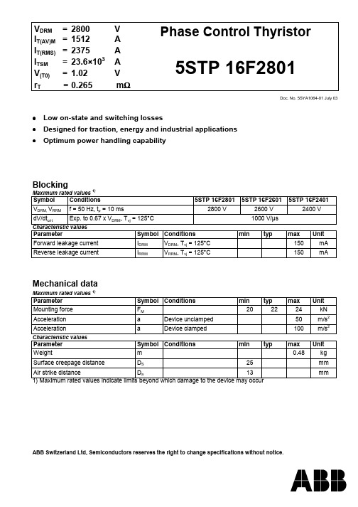
V DRM=2800VI T(AV)M=1512AI T(RMS)=2375AI TSM=23.6×10³AV(T0)=1.02Vr T=0.265mΩPhase Control Thyristor5STP 16F2801Doc. No. 5SYA1064-01 July 03•Low on-state and switching losses•Designed for traction, energy and industrial applications•Optimum power handling capabilityBlockingMaximum rated values 1)Symbol Conditions5STP 16F28015STP 16F26015STP 16F2401 V DRM, V RRM f = 50 Hz, t p = 10 ms2800 V2600 V2400 VdV/dt crit Exp. to 0.67 x V DRM, T vj = 125°C1000 V/µsCharacteristic valuesParameter Symbol Conditions min typ max UnitForward leakage current I DRM V DRM, T vj = 125°C150mA Reverse leakage current I RRM V RRM, T vj = 125°C150mAMechanical dataMaximum rated values 1)Parameter Symbol Conditions min typ max UnitMounting force F M202224kN Acceleration a Device unclamped50m/s2 Acceleration a Device clamped100m/s2 Characteristic valuesParameter Symbol Conditions min typ max UnitWeight m0.48kg Surface creepage distance D S25mm Air strike distance D a13mm1) Maximum rated values indicate limits beyond which damage to the device may occur元器件交易网ABB Switzerland Ltd, Semiconductors reserves the right to change specifications without notice.On-stateMaximum rated values1)ParameterSymbol Conditions min typ max Unit Average on-state current I T(AV)M Half sine wave, T c = 70°C 1512A RMS on-state current I T(RMS)2375A Peak non-repetitive surge currentI TSM 23.60×10³A Limiting load integral I 2t tp = 10 ms, T vj = 125 °C,V D = V R = 0 V2.79×106A 2s Peak non-repetitive surge currentI TSM 25.20×10³A Limiting load integralI 2ttp = 8.3 ms, T vj = 125 °C,V D = V R = 0 V2.64×106A 2s Characteristic valuesParameter Symbol Conditions mintypmaxUnit On-state voltage V T I T = 2000 A, T vj = 125 °C 1.55V Threshold voltage V (T0) 1.02V Slope resistance r T I T = 1900 A - 5800 A, T vj = 125 °C0.265m ΩHolding current I H T vj = 25 °C 170mA T vj = 125 °C 90mA Latching currentI LT vj = 25 °C 450mA T vj = 125 °C350mASwitchingMaximum rated values1)ParameterSymbol Conditions min typ maxUnit Critical rate of rise of on-state currentdi/dt crit Cont.f = 50 Hz 200A/µs Critical rate of rise of on-state currentdi/dt critT vj = 125 °C,I T = I T(AV),V D ≤ 0.67 V DRM ,I FG = 2 A, t r = 0.3 µsCont.f = 1 Hz1000A/µs Circuit-commutated turn-off timet q T vj = 125°C, I TRM = 2000 A,V R = 200 V, di T /dt = -12.5 A/µs,V D ≤ 0.67⋅V DRM , dv D /dt = 50V/µs200µsCharacteristic valuesParameter Symbol Conditions mintyp max Unit Recovery chargeQ rrT vj = 125°C, I TRM = 2000 A,V R = 200 V,di T /dt = -12.5 A/µs2600µAsGate turn-on delay time t gd V D = 0.4⋅V RM , I FG = 2 A, t r = 0.3 µs, T vj = 25 °C2µsTriggeringMaximum rated values1)ParameterSymbol Conditions min typ max Unit Peak forward gate voltage V FGM 12V Peak forward gate current I FGM 10A Peak reverse gate voltage V RGM 10V Mean forward gate powerP G(AV)3W Characteristic valuesParameter Symbol Conditions min typ maxUnit Gate-trigger voltageV GTT vj = -40 °C T vj = 25 °C T vj = 125 °C0.25432VGate-trigger current I GT T vj = -40 °C T vj = 25 °C T vj = 125 °C10500250150mAThermalMaximum rated values1)Parameter Symbol Conditions min typ max Unit Operating junction temperature rangeT vj-40125°C Storage temperature range T stg -40125°C Characteristic valuesParameterSymbol Conditionsmintyp max Unit Thermal resistance junction to caseR th(j-c)Double-side cooled 16K/kW R th(j-c)A Anode-side cooled 25K/kW R th(j-c)CCathode-side cooled 45K/kW Thermal resistance case to heatsinkR th(c-h)Double-side cooled 4K/kW R th(c-h)Single-side cooled8K/kWAnalytical function for transient thermalimpedance:)e -(1R = (t)Z n1i t/-i c)-th(j i å=τi 1234R i (K/kW) 5.5007.240 2.000 1.340τi (s)0.46530.15330.03750.0034Fig. 1 Transient thermal impedance junction-to case.Fig. 2Max. on-state voltage characteristics Fig. 3Surge forward current vs. pulse length. Halfsine wave, single pulse, V R = 0 VFig. 4Forward power loss vs. average forward current, sine waveform, f = 50 Hz, T = 1/f Fig. 5Forward power loss vs. average forward current, square waveform, f = 50 Hz, T = 1/fFig. 6Max. case temperature vs.average forward current, sine waveform, f = 50Hz, T = 1/f Fig. 7Max. case temperature vs.average forward current, square waveform, f = 50Hz, T = 1/fABB Switzerland Ltd, Semiconductors reserves the right to change specifications without notice.ABB Switzerland Ltd Doc. No. 5SYA1064-01 July 03Semiconductors Fabrikstrasse 3CH-5600 Lenzburg, Switzerland Telephone +41 (0)58 586 1419Fax +41 (0)58 586 1306RED WHITEFig. 8Device Outline Drawing.。
ZR36016中文资料(List Unclassifed)中文数据手册「EasyDatasheet - 矽搜」

ZR36050 Compression
PXOUT
Color Space Conversion
PXIN
Format Conversion
Window Management Block-to-Raster
ZR36050 Expansion
图 1. ZR36016操作与 ZR36050
PXOUT
芯片中文手册,看全文,戳
锡永,一到像素输出总线,另外给光栅到 块转换器.每个路径上数据可以独立地 经历格式转换,而在这种情况下指reso由抽取或内插,lution变换 色度分量;例如,抽取从
Color Space Conversion
PXIN
Format Conversion
Window Management Raster-to-Block
与ZR36050数据传输速率为最大30兆赫,系统时钟速率.像 素总线传输以最大30兆赫4:0:0,或在系统时钟1,1/2或1 /4为其他格式频率比,具体取决于所选择格式转换.
如图2中,输入像素数据通过一个多 路开关,颜色空间转换器.在压缩,这 复用器总是传递像素数据(顶端输入).该
颜色空间转换器输出取入压缩两个路径
在延迟元件装置示出,处理流水线延迟从象素输入到输出被 防护持恒定,即使彩色空间转换被旁路.输入水平和垂直同步信 号经历相同延迟后输出.
ZR36016和操作参数操作模式由控制寄存器,它们是从主机 接口编程确定.有两种模式控制压缩和扩张:单帧模式 和顺序模式.在单一帧模式中,ZR36016上执行(对于交错
GO / STOP注册
读写 初始值 功能
直接地址:0×00
0x00
注册并启用停止处理
ZR36016.
7
A3516LUA资料

ELECTRICAL CHARACTERISTICS over operating temperature range, at VCC = 5 V (unless otherwise noted).
Characteristic Supply Voltage Supply Current Quiescent Voltage Output
2
Worcester, Massachusetts 01615-0036 (508) 853-5000
Copyright © 1996, 2003 Allegro MicroSystems, Inc.
元器件交易网
3515 AND 3516 RATIOMETRIC,
LINEAR HALL-EFFECT SENSORS
NOTE: For detailed information on purchasing options, contact your local Allegro field applications engineer or sales representative.
Allegro MicroSystems, Inc. reserves the right to make, from time to time, revisions to the anticipated product life cycle plan for a product to accommodate changes in production capabilities, alternative product availabilities, or market demand. The information included herein is believed to be accurate and reliable. However, Allegro MicroSystems, Inc. assumes no responsibility for its use; nor for any infringements of patents or other rights of third parties which may result from its use.
MEMORY存储芯片M25P16-VMN3TPB中文规格书

Features•SPI bus compatible serial interface •16Mb Flash memory•75 MHz clock frequency (maximum)•2.7V to 3.6V single supply voltage•Page program (up to 256 bytes) in 0.64ms (TYP)•Erase capability–Sector erase: 512Kb in 0.6 s (TYP)–Bulk erase: 16Mb in 13 s (TYP)•Write protection–Hardware write protection: protected area size defined by non-volatile bits BP0, BP1, BP2•Deep power down: 1µA (TYP)•Electronic signature–JEDEC standard 2-byte signature (2015h)–Unique ID code (UID) and 16 bytes of read-only data, available upon customer request–RES command, one-byte signature (14h) for backward compatibility•More than 100,000 write cycles per sector •More than 20 years data retention •Automotive grade parts available •Packages (RoHS compliant)–SO8N (MN) 150 mils –SO8W (MW) 208 mils –SO16 (MF) 300 mils–VFDFPN8 (MP) MLP8 6mm x 5mm –VFDFPN8 (ME) MLP8 8mm x 6mm –UFDFPN8 (MC) MLP8 4mm x 3mm找Memory 、FPGA 、二三极管、连接器、模块、光耦、电容电阻、单片机、处理器、晶振、传感器、 滤波器,上深圳市美光存储技术有限公司Functional DescriptionThe M25P16 is an 16Mb (2Mb x 8) serial Flash memory device with advanced write pro-tection mechanisms accessed by a high speed SPI-compatible bus. The device supportshigh-performance commands for clock frequency up to 75MHz.The memory can be programmed 1 to 256 bytes at a time using the PAGE PROGRAMcommand. It is organized as 32 sectors, each containing 256 pages. Each page is 256bytes wide. Memory can be viewed either as 8,192 pages or as 2,097,152 bytes. The en-tire memory can be erased using the BULK ERASE command, or it can be erased onesector at a time using the SECTOR ERASE command.This datasheet details the functionality of the M25P16 device based on 110nm process.Figure 2: Pin Connections: SO8, VFQFPN , VDFPN1234V CC HOLD#5678DQ1V SSS#DQ0C W#Note:1.There is an exposed central pad on the underside of the MLP8 package that is pulled in-ternally to V SS , and must not be connected to any other voltage or signal line on the PCB. The Package Mechanical section provides information on package dimensions and how to identify pin 1.Figure 3: Pin Connections: SO16123416151413V CC HOLD#DNU DNU DNU DNU DNU DNU DNU DNU 56781211109DQ1V SS S#DQ0C W#/V PPNotes:1.DU = Don't Use2.The Package Mechanical section provides information on package dimensions and howto identify pin 1.Operating FeaturesPage ProgrammingTo program one data byte, two commands are required: WRITE ENABLE, which is onebyte, and a PAGE PROGRAM sequence, which is four bytes plus data. This is followed bythe internal PROGRAM cycle of duration t PP. To spread this overhead, the PAGE PRO-GRAM command allows up to 256 bytes to be programmed at a time (changing bitsfrom 1 to 0), provided they lie in consecutive addresses on the same page of memory. Tooptimize timings, it is recommended to use the PAGE PROGRAM command to programall consecutive targeted bytes in a single sequence than to use several PAGE PROGRAMsequences with each containing only a few bytes.Status RegisterThe status register contains a number of status and control bits that can be read or set(as appropriate) by specific commands. For a detailed description of the status registerbits, see READ STATUS REGISTER (page 25).Data Protection by ProtocolNon-volatile memory is used in environments that can include excessive noise. The fol-lowing capabilities help protect data in these noisy environments.Power on reset and an internal timer (t PUW) can provide protection against inadvertentchanges while the power supply is outside the operating specification.PROGRAM, ERASE, and WRITE STATUS REGISTER commands are checked before theyare accepted for execution to ensure they consist of a number of clock pulses that is amultiple of eight.All commands that modify data must be preceded by a WRITE ENABLE command to setthe write enable latch (WEL) bit.In addition to the low power consumption feature, the DEEP POWER-DOWN mode of-fers extra software protection since all PROGRAM, and ERASE commands are ignoredwhen the device is in this mode.Software Data ProtectionMemory can be configured as read-only using the block protect bits (BP2, BP1, BP0) asshown in the Protected Area Sizes table.Hardware Data ProtectionHardware data protection is implemented using the write protect signal applied on theW# pin. This freezes the status register in a read-only mode. In this mode, the block pro-tect (BP) bits and the status register write disable bit (SRWD) are protected.Table 3: Protected Area SizesNote: 1.0 0 = unprotected area (sectors): The device is ready to accept a BULK ERASE commandonly if all block protect bits (BP1, BP0) are 0.Table 4: Protected Area Sizes。
东芝TAR5S××系列新型稳压集成电路

1 . 5
VN _ O4
3 O 1 0 O1 . 2
V V
u A u A
屯子 世 界
— —
・ቤተ መጻሕፍቲ ባይዱ 0 2 1. 02
1 — 6 —
新 器件 应 用 ・
2 。 5 C。
C 1J 、 输 出 端 4脚 C u 1 J . IF o = 0IF3脚 T 外 所 接 噪 声 抑 制 电 容 C。E 00 、 NS I .1J = IF
功耗 ( 装 在 3 mm O 安 0 X3 mm 玻 璃环 氧 电路 板上 ) P2 D
工 作 温度 存 储 温度 T p or T t sg
推荐应 用 电路
应 用 电路 如 图 4所 示 , 如果 不 使 用 控
表 3中 各 点 稳 压 器 的输 入 电压 V
各 自的 稳压 输 出 电压 VoT 1 、 出 电 流 制 端 ( +V输 U 1脚 )东 芝 公 司 建 议 把 此 引脚 与 电 , I=0 o 5 mA、 输 入 端 5 脚 外 接 电 容 压 输 入 端 ( 脚 ) 相 连 。  ̄ 5 V CN 1 、 输 出 端 4脚 C U 0LF 3脚 . F = u o =1 、 T J
号对照 , 请查阅后面 的表 4 稳压输出明细 “
表 1 极 限工 作 参 数 ( a 2 o 、 T = 5c) 名 称 输 入 电压 输 出 电流
功耗 ( 无散 热 片 ) 表 ” 它 们 的 各 引脚 排 列 和 功 能 如 图 3所 。
符号 VN l IT O U
P1 D
符号 VU OT
测 试 条 件 请参阅《 稳压 输 出 明细 表》
TAR5S19中文资料

TOSHIBA Bipolar Linear Integrated Circuit Silicon MonolithicTAR5S15~TAR5S50Point Regulators (Low-Dropout Regulator)The TAR5Sxx Series is comprised of general-purpose bipolar single-power-supply devices incorporating a control pin which can be used to turn them ON/OFF.Overtemperature and overcurrent protection circuits are built in to the devices’ output circuit.Features• Low stand-by current•Overtemperature/overcurrent protection • Operation voltage range is wide. • Maximum output current is high.• Difference between input voltage and output voltage is low. • Small package.• Ceramic capacitors can be used.Pin Assignments (top view)Overtemperature protection and overcurrent protection functions are not necessary guarantee of operating ratings below the absolute maximum ratings.Do not use devices under conditions in which their absolute maximum ratings will be exceeded.Weight: 0.014 g (typ.)1 32 V IN NOISE4GND V OUT CONTROL 5List of Products Number and MarkingMarking on the ProductProducts No.MarkingProducts No.MarkingTAR5S15 1V5 TAR5S33 3V3 TAR5S16 1V6 TAR5S34 3V4 TAR5S17 1V7 TAR5S35 3V5 TAR5S18 1V8 TAR5S36 3V6 TAR5S19 1V9 TAR5S37 3V7 TAR5S20 2V0 TAR5S38 3V8 TAR5S21 2V1 TAR5S39 3V9 TAR5S22 2V2 TAR5S40 4V0 TAR5S23 2V3 TAR5S41 4V1 TAR5S24 2V4 TAR5S42 4V2 TAR5S25 2V5 TAR5S43 4V3 TAR5S26 2V6 TAR5S44 4V4 TAR5S27 2V7 TAR5S45 4V5 TAR5S28 2V8 TAR5S46 4V6 TAR5S29 2V9 TAR5S47 4V7 TAR5S30 3V0 TAR5S48 4V8 TAR5S31 3V1 TAR5S49 4V9 TAR5S32 3V2 TAR5S50 5V0Absolute Maximum Ratings (Ta = 25°C)Characteristics Symbol Rating UnitSupply voltage V IN 15 V Output current I OUT 200 mA 200 (Note 1)Power dissipationP D 380 (Note 2)mWOperation temperature range T opr −40 to 85 °C Storage temperature rangeT stg−55 to 150°CNote:Using continuously under heavy loads (e.g. the application of high temperature/current/voltage and thesignificant change in temperature, etc.) may cause this product to decrease in the reliability significantly even if the operating conditions (i.e. operating temperature/current/voltage, etc.) are within the absolute maximum ratings and the operating ranges.Please design the appropriate reliability upon reviewing the Toshiba Semiconductor Reliability Handbook (“Handling Precautions”/“Derating Concept and Methods”) and individual reliability data (i.e. reliability test report and estimated failure rate, etc).Note 1: Unit RatintgNote 2: Mounted on a glass epoxy circuit board of 30 × 30 mm. Pad dimension of 50 mm 23 V 0Example: TAR5S30 (3.0 V output)TAR5S15~TAR5S22Electrical Characteristic (unless otherwise specified, V IN= V OUT+ 1 V, I OUT= 50 mA,C IN= 1 μF, C OUT= 10 μF, C NOISE= 0.01 μF, T j= 25°C)Characteristics SymbolTestConditionMinTyp.Max Unit Output voltage V OUT Please refer to the Output Voltage Accuracy table.Line regulation Reg・line V OUT+ 1 V < = VIN< = 15 V,I OUT= 1 mA⎯ 3 15 mV Load regulation Reg・load 1mA< = I OUT< = 150 mA ⎯ 25 75 mVI B1 I OUT= 0 mA ⎯ 170 ⎯Quiescent currentI B2I OUT= 50 mA ⎯ 550 850μA Stand-by current I B (OFF)V CT= 0 V ⎯⎯ 0.1 μAOutput noise voltage V NO V IN= V OUT+ 1 V, I OUT= 10 mA,10 Hz< = f< = 100 kHz,C NOISE= 0.01 μF, Ta = 25°C⎯ 30 ⎯μV rmsTemperature coefficient T CVO−40°C< = T opr< = 85°C ⎯ 100 ⎯ ppm/°C Input voltage V IN⎯ 2.4⎯ 15 VRipple rejection R.R. V IN= V OUT+ 1 V, I OUT= 10 mA,C NOISE= 0.01 μF, f = 1 kHz,V Ripple= 500 mV p-p, Ta = 25°C⎯ 70 ⎯ dBControl voltage (ON) V CT (ON)⎯ 1.5⎯V IN V Control voltage (OFF) V CT (OFF)⎯⎯⎯ 0.4 VControl current (ON) I CT (ON)V CT= 1.5 V ⎯ 3 10 μAControl current (OFF) I CT (OFF)V CT= 0 V ⎯ 0 0.1 μATAR5S23~TAR5S50Electrical Characteristic (unless otherwise specified, V IN= V OUT+ 1 V, I OUT= 50 mA,C IN= 1 μF, C OUT= 10 μF, C NOISE= 0.01 μF, T j= 25°C)Characteristics SymbolTestConditionMinTyp.Max Unit Output voltage V OUT Please refer to the Output Voltage Accuracy table.Line regulation Reg・line V OUT+ 1 V < = VIN< = 15 V,I OUT= 1 mA⎯ 3 15 mV Load regulation Reg・load 1mA< = I OUT< = 150 mA ⎯ 25 75 mVI B1 I OUT= 0 mA ⎯ 170 ⎯Quiescent currentI B2I OUT= 50 mA ⎯ 550 850μA Stand-by current I B (OFF)V CT= 0 V ⎯⎯ 0.1 μAOutput noise voltage V NO V IN= V OUT+ 1 V, I OUT= 10 mA,10 Hz< = f< = 100 kHz,C NOISE= 0.01 μF, Ta = 25°C⎯ 30 ⎯μV rmsDropout volatge V IN− V OUT I OUT= 50 mA ⎯ 130 200mV Temperature coefficient T CVO−40°C< = T opr< = 85°C ⎯ 100 ⎯ ppm/°CInput voltage V IN⎯V OUT+ 0.2 V ⎯ 15 VRipple rejection R.R. V IN= V OUT+ 1 V, I OUT= 10 mA,C NOISE= 0.01 μF, f = 1 kHz,V Ripple= 500 mV p-p, Ta = 25°C⎯ 70 ⎯ dBControl voltage (ON) V CT (ON)⎯ 1.5⎯V IN V Control voltage (OFF) V CT (OFF)⎯⎯⎯ 0.4 V Control current (ON) I CT (ON)V CT= 1.5 V ⎯ 3 10 μA Control current (OFF) I CT (OFF)V CT= 0 V ⎯ 0 0.1 μAOutput Voltage Accuracy(V IN = V OUT + 1 V, I OUT = 50 mA, C IN = 1 μF, C OUT = 10 μF, C NOISE = 0.01 μF, T j = 25°C)Product No.SymbolMinTyp.MaxUnitTAR5S15 1.44 1.5 1.56 TAR5S16 1.54 1.6 1.66 TAR5S17 1.64 1.7 1.76 TAR5S18 1.74 1.8 1.86 TAR5S19 1.84 1.9 1.96 TAR5S20 1.94 2.0 2.06 TAR5S21 2.04 2.1 2.16 TAR5S22 2.14 2.2 2.26 TAR5S23 2.24 2.3 2.36 TAR5S24 2.34 2.4 2.46 TAR5S25 2.43 2.5 2.57 TAR5S26 2.53 2.6 2.67 TAR5S27 2.63 2.7 2.77 TAR5S28 2.73 2.8 2.87 TAR5S29 2.83 2.9 2.97 TAR5S30 2.92 3.0 3.08 TAR5S31 3.02 3.1 3.18 TAR5S32 3.12 3.2 3.28TAR5S33 3.21 3.3 3.39 TAR5S34 3.31 3.4 3.49 TAR5S35 3.41 3.5 3.59 TAR5S36 3.51 3.6 3.69 TAR5S37 3.6 3.7 3.8 TAR5S38 3.7 3.8 3.9 TAR5S39 3.8 3.9 4.0 TAR5S40 3.9 4.0 4.1 TAR5S41 3.99 4.1 4.21 TAR5S42 4.09 4.2 4.31 TAR5S43 4.19 4.3 4.41 TAR5S44 4.29 4.4 4.51 TAR5S45 4.38 4.5 4.62 TAR5S46 4.48 4.6 4.72 TAR5S47 4.58 4.7 4.82 TAR5S48 4.68 4.8 4.92 TAR5S49 4.77 4.9 5.03 TAR5S50V OUT 4.87 5.0 5.13VApplication Note1. Recommended Application CircuitThe figure above shows the recommended configuration for using a point regulator. Insert a capacitor for stable input/output operation. If the control function is not to be used, Toshiba recommend that the control pin (pin 1) be connected to the V CC pin.2. Power DissipationThe power dissipation for board-mounted TAR5Sxx Series devices (rated at 380 mW) is measured using a board whose size and pattern are as shown below. When incorporating a device belonging to this series into your design, derate the power dissipation as far as possible by reducing the levels of parameters such as input voltage, output current and ambient temperature. Toshiba recommend that these devices should typically be derated to 70%~80% of their absolute maximum power dissipation value.Thermal Resistance Evaluation BoardCircuit board material: glass epoxy, Circuit board dimension:30 mm × 30 mm, Copper foil pad area: 50 mm 2(t = 0.8 mm)NOISEGND CONTROLControl LevelOperationHIGH ONLOW OFF3. Ripple RejectionThe devices of the TAR5Sxx Series feature a circuit with an excellent ripple rejection characteristic. Because the circuit also features an excellent output fluctuation characteristic for sudden supply voltage drops, the circuit is ideal for use in the RF blocks incorporated in all mobile telephones.4. NOISE PinTAR5Sxx Series devices incorporate a NOISE pin to reduce output noise voltage. Inserting a capacitorbetween the NOISE pin and GND reduces output noise. To ensure stable operation, insert a capacitor of 0.0047 μF or more between the NOISE pin and GND.The output voltage rise time varies according to the capacitance of the capacitor connected to the NOISE pin.Ripple Rejection − fTAR5S28 Input Transient ResponseFrequency f (Hz)Time t (ms)R i p p l e r e j e c t i o n (d B )C NOISE − V NTurn On WaveformNOISE capacitance C NOISE (F)Time t (ms)Co n t r o l v o l t a g e V C T (O N ) (V )O u t p u t n o i s e v o l t a g e V N (μV )μO u t p u t v o l t a g e V O U T (V )1458 10236 7 95. Example of Characteristics when Ceramic Capacitor is UsedShown below is the stable operation area, where the output voltage does not oscillate, evaluated using a Toshiba evaluation circuit. The equivalent series resistance (ESR) of the output capacitor and output current determines this area. TAR5Sxx Series devices operate stably even when a ceramic capacitor is used as the output capacitor.If a ceramic capacitor is used as the output capacitor and the ripple frequency is 30 kHz or more, the ripple rejection differs from that when a tantalum capacitor is used. This is shown below.Toshiba recommend that users check that devices operate stably under the intended conditions of use.Examples of safe operating area characteristicsEvaluation Circuit for Stable Operating AreaRipple Rejection Characteristic (f = 10 kHz~300 kHz)(TAR5S15) Stable Operating AreaOutput current I OUT (mA)(TAR5S50) Stable OperatingArea(TAR5S28) Stable Operating AreaOutput current I OUT (mA)Output current I OUT (mA)E q u i v a l e n t s e r i e s r e s i s t a n c e E S R (Ω)E q u i v a l e n t s e ri e s r e s i s t a n c e E S R (Ω)E q u i v a l e n t s e r i e s r e s i s t a n c e E S R (Ω)R i p p l e r e j e c t i o n (d B )(TAR5S30) Ripple Rejection – fFrequency f (Hz)V IN = V +F OUTCapacitors used for evaluationMade by Murata C IN : GRM40B105KC OUT : GRM40B105K/GRM40B106KO u t p u t v o l t a g e V O U T (V )Ou t p u t v o l t a g eV O U T (V )Output current I OUT (mA)(TAR5S15) I OUT – V OUTOu t p u t v o l t a g eV O U T (V )Output current I OUT (mA)(TAR5S18) I OUT – V OUTOu t p u t v o l t a ge V O U T (V )Output current I OUT (mA)(TAR5S20) I OUT – V OUTOu t p u t v o l t ag e V O U T(V )Output current I OUT(mA)(TAR5S21) I OUT – V OUTOutput currentI OUT (mA)(TAR5S22) I OUT – V OUTOutput current I OUT (mA)(TAR5S23) I OUT – V OUTO u t p u t v o l t a g e V O U T (V )Output current I OUT (mA)(TAR5S27) I OUT – V OUTO u t p u t v o l t a g e V O U T (V )Output current I OUT (mA)(TAR5S30)I OUT – V OUTO u t p u t v o l t a g e V O U T (V )Output currentI OUT (mA)(TAR5S25) I OUT – V OUTOu t p u t v o l t a g e V O U T (V )Output current I OUT (mA)(TAR5S31) I OUT – V OUTO u t p u t v o l t a g e V O U T (V )Output current I OUT (mA)(TAR5S28) I OUT – V OUTO u t p u t v o l t a g e V O U T (V )Output current I OUT (mA)(TAR5S29) I OUT – V OUTO u t p u t v o l t a g e V O U T (V )Output current I OUT (mA)(TAR5S32)I OUT – V OUTOu t p u t v o l t ag e V O U T (V )Output current I OUT (mA)(TAR5S33)I OUT – V OUTO u t p u t v o l t a g e V O U T (V )50 100 150Output current I OUT (mA)(TAR5S45) I OUT – V OUTO u t p u t v o l t a g e V O U T (V )0 50 100 150Output current I OUT (mA)(TAR5S50) I OUT – V OUTO u t p u t v o l t a g e V O U T (V )Output current I OUT (mA)(TAR5S35) I OUT – V OUTO u t p u t v o l t a g e V O U T (V )0 50 100 150Output current I OUT (mA)(TAR5S48) I OUT – V OUTO u t p u t v o l t a g e 圧 V O U T (V )0 50 100 150B i a s c u r r e n t I B (m A )B i a s c u r r e nt I B (m A )Input voltage V IN (V)(TAR5S15)I B – VINB i a s c u r r e nt I B (m A )Input voltage V IN (V)(TAR5S18)I B – VINB i a s c u r re n t I B (m A )Input voltage V IN (V)(TAR5S20)I B – VINB i a s c u r r en t I B(m A )Input voltage V IN (V)(TAR5S21)IB – V INInput voltageV IN (V)(TAR5S22)I B – V INInput voltage V IN (V)(TAR5S23)I B – V INB i a s c u r r e n t I B (m A )Input voltage V IN (V)(TAR5S27)I B – V INB i a s c u r r e n t I B (m A )Input voltage V IN (V)(TAR5S30)I B – V INB i a s c u r r e n t I B (m A )Input voltageV IN (V)(TAR5S25)I B – V INB i a s c u r r e n t I B (m A )Input voltage V IN (V)(TAR5S31)I B – V INB i a s c u r r e n t I B (m A )Input voltage V IN (V)(TAR5S28)I B – V INB i a s c u r r e n t I B (m A )Input voltage V IN (V)(TAR5S29)I B – V INB i a s c u r r e n t I B (m A )Input voltage V IN (V)(TAR5S32)I B – V INB i a s c u r re n t I B (m A )Input voltage V IN (V)(TAR5S33)I B – V INB i a s c u r r e n t I B (m A )Input voltage V IN (V)(TAR5S45)I B – V INB i a s c u r r e n t I B (m A )Input voltage V IN (V)(TAR5S50) I B – V INB i a s c u r r e n t I B (m A )Input voltage V IN (V)(TAR5S35)I B – V INB i a s c u r r e n t I B (m A )Input voltage V IN (V)(TAR5S48) I B – V INB i a s c u r r e n t I B (m A )O u t p u t v o l t a g e V O U T (V )O ut p u t v o l t a g eV O U T (V )Input voltage V IN (V)(TAR5S15)V OUT – V INOut p u t v o l t a g eV O U T (V )Input voltage V IN (V)(TAR5S18)V OUT – V INOu t p u t v o l t a ge V O U T (V )Input voltage V IN (V)(TAR5S20)V OUT – V INOut p u t v o l t ag e V O U T(V )Input voltage V IN (V)(TAR5S21)VOUT – V INInput voltage VIN (V)(TAR5S22)V OUT – V INInput voltage V IN (V)(TAR5S23)V OUT – V INO u t p u t v o l t a g e V O U T (V )Input voltage V IN (V)(TAR5S27)V OUT – V INO u t p u t v o l t a g e V O U T (V )0 5 10 15Input voltage V IN(V)(TAR5S30)V OUT – V INO u tp u t v o l t a g e V O U T (V )Input voltage V IN (V)(TAR5S25)V OUT – V INO u t p u t v o l t a g e V O U T (V )Input voltage V IN(V)(TAR5S31)V OUT – V INO u t p u t vo l t a g e V O U T (V )Input voltage V IN (V)(TAR5S28)V OUT – V INO u t p u t v o l t a g e V O U T (V )0 5 10 15Input voltage V IN (V)(TAR5S29)V OUT – V INO u t p u t v o l t a g e V O U T (V )Input voltage V IN (V)(TAR5S33)V OUT – V INO u t p u t v o l t a g e V O U T (V )0 5 10 15Input voltage V IN (V)(TAR5S32)V OUT – V INO u t p u t v o l t a g e V O U T (V )Input voltage V IN (V)(TAR5S45)V OUT – V INO u t p u t v o l t a g e V O U T (V )Input voltage V IN (V)(TAR5S50)V OUT – V INO u t p u t v o l t a g e V O U T (V )Input voltage V IN (V)(TAR5S48)V OUT – V INO u t p u tv ol t a g e V O U T (V )0 5 10 156Input voltage V IN (V)(TAR5S35)V OUT – V INO u t p ut v o l t a g e V O U T (V )O u t p u t v o l t a g e V O U T (V )O ut p u t v ol t a g e V O U T (V )Ambient temperature Ta (°C)(TAR5S15)V OUT – TaOu t p u t v ol t a g e V O U T (V )Ambient temperature Ta (°C)(TAR5S18)V OUT – TaOu t p u tv o l t a g e V O U T (V )Ambient temperature Ta (°C)(TAR5S20)V OUT – TaO ut p u tv o l t a g eVO U T (V )Ambient temperature Ta (°C)(TAR5S21)V OUT – TaAmbient temperature Ta (°C)(TAR5S22)V OUT – TaAmbient temperature Ta (°C)(TAR5S23)V OUT – TaO u t p u t v o l t a g e V O U T (V )Ambient temperature Ta (°C)(TAR5S25)V OUT – TaO u t p u t v o l t a g e V O U T (V )−50−25 0 25 10075 50Ambient temperature Ta (°C)(TAR5S27)V OUT – TaO u t p u t v o l t a g e V O U T (V )−50−25 0 25 10075 50Ambient temperature Ta (°C)(TAR5S30)V OUT – TaO u t p u t v o l t a g eV O U T(V )Ambient temperature Ta (°C)(TAR5S31)V OUT – TaO u t p u t v o l t a g e V O U T (V )Ambient temperature Ta (°C)(TAR5S28)V OUT – TaO u t p u t v o l t a g e V O U T (V )−50−25 0 2510075 50Ambient temperature Ta (°C)(TAR5S29)V OUT – TaO u t p u t v o l t a g e V O U T (V )−50−25 0 25 10075 50Ambient temperature Ta (°C)(TAR5S32)V OUT – TaO ut p u tv o l t a g e V O U T (V )Ambient temperature Ta (°C)(TAR5S33)V OUT – TaO u t p u t v o l t a g e V O U T (V )−50−25 0 2575 50100Ambient temperature Ta (°C)(TAR5S45)V OUT – TaO u t p u t v o l t a g eV O UT (V )Ambienttemperature Ta (°C)(TAR5S50)V OUT – TaO u t p u t v o l t a g e VO UT (V )Ambienttemperature Ta (°C)(TAR5S35)V OUT – TaO u t p u t v o l t a g e V O U T (V )Ambient temperature Ta (°C)(TAR5S48)V OUT – TaO u t p u t v o l t a g e V O U T (V )−50−25 0 25 10075 50−50−25 0 25 10075 50Ambient temperature Ta (°C)I B – TaBiascurrentIB(mA)Ambient temperature Ta (°C)(TAR5S23~TAR5S50) V IN - V OUT – TaDropoutvoltageVIN-VOUT(V)Output current IOUT(mA)(TAR5S23~TAR5S50) V IN - V OUT – I OUTDropoutvoltageVIN-VOUT(V)Output current I OUT(mA)I B – I OUTBiascurrentIB(mA)Time t (ms)Turn On WaveformOutputvoltageVOUT(V)Time t (ms)Turn Off WaveformOutputvoltageVOUT(V)231123ControlvoltageVCT(ON)(V)ControlvoltageVCT(ON)(V)Ambient temperature Ta (°C)P D – TaP o w e r d i s s i p a t i o n P D (m W )−400 4012080Frequency f (Hz)V N – fO u t p u t n o i s e v o l t a g e V N (μV / H z )10100 1 k 10 k 100 kFrequency f (Hz)Ripple Rejection – fR i p p l e r e j e c t i o n (d B )10 100 1 k 10 k100 k 1000 kPackage DimensionsWeight: 0.014 g (typ.)RESTRICTIONS ON PRODUCT USE20070701-EN GENERAL •The information contained herein is subject to change without notice.•TOSHIBA is continually working to improve the quality and reliability of its products. Nevertheless, semiconductor devices in general can malfunction or fail due to their inherent electrical sensitivity and vulnerability to physical stress. It is the responsibility of the buyer, when utilizing TOSHIBA products, to comply with the standards of safety in making a safe design for the entire system, and to avoid situations in which a malfunction or failure of such TOSHIBA products could cause loss of human life, bodily injury or damage to property.In developing your designs, please ensure that TOSHIBA products are used within specified operating ranges as set forth in the most recent TOSHIBA products specifications. Also, please keep in mind the precautions and conditions set forth in the “Handling Guide for Semiconductor Devices,” or “TOSHIBA Semiconductor Reliability Handbook” etc.• The TOSHIBA products listed in this document are intended for usage in general electronics applications (computer, personal equipment, office equipment, measuring equipment, industrial robotics, domestic appliances, etc.).These TOSHIBA products are neither intended nor warranted for usage in equipment that requires extraordinarily high quality and/or reliability or a malfunction or failure of which may cause loss of human life or bodily injury (“Unintended Usage”). Unintended Usage include atomic energy control instruments, airplane or spaceship instruments, transportation instruments, traffic signal instruments, combustion control instruments, medical instruments, all types of safety devices, etc.. Unintended Usage of TOSHIBA products listed in his document shall be made at the customer’s own risk.•The products described in this document shall not be used or embedded to any downstream products of which manufacture, use and/or sale are prohibited under any applicable laws and regulations.• The information contained herein is presented only as a guide for the applications of our products. No responsibility is assumed by TOSHIBA for any infringements of patents or other rights of the third parties which may result from its use. No license is granted by implication or otherwise under any patents or other rights of TOSHIBA or the third parties.• Please contact your sales representative for product-by-product details in this document regarding RoHS compatibility. Please use these products in this document in compliance with all applicable laws and regulations that regulate the inclusion or use of controlled substances. Toshiba assumes no liability for damage or losses occurring as a result of noncompliance with applicable laws and regulations.。
洛雷斯(Lorex)16通道2TB硬盘DVR系列产品说明书

WATCH OVER YOUR WORLDFROM ANYWHERE IN THE WORLDDon’t miss a thing with true-to-life video in real-time. LorexStratus Connectivity offers instant connection anywhere yougo with no recurring fees.162TBChannels 960H900TVL ResolutionHDD•Tablet / smartphone viewing and playback 1 •Lorex Stratus Connectivity - 3 step setup•Superior 960H Resolution - 34% more detailed and true-to-life images 2 •Real-time recording at 30fps per channel •24/7 security-grade hard drive•Instant email alerts with snap shot attachment •Continuous, scheduled and motion recording•Advanced mobile apps with live viewing, playback, video recording, and snap shot •PC and Mac compatible•HDMI cable included for simple connection to HD TVs 3 •H.264 video compression 4•Pentaplex operation - view, record, playback, back up & remotely control the system simultaneously •PTZ cameras supported (RS485). Remotely control through App •Accurate time stamps with NTP & Daylight Savings Time •3 video outputs (HDMI, VGA and BNC) to connect multiple monitors•Automatic firmware upgrades over Internet ensure your system is secure and up to date 5DVR FEATURES:130/90FT Night Vision900TVL ResolutionIP66•1.3 Megapixel image sensor (900 TVL resolution)•Lightweight yet extremely durable Polycarbonate housing•Integrated automatic Infrared Cut Filter (ICR) ensures accurate color representation in all lighting conditions •Day/Night mode: Picture automatically switches to B&W delivering better clarity in low light conditions •BrightNight viewing with enhanced low light image sensor•Close-up recognition at night with auto light compensation prevents wash-out effect•Night vision range up to 130ft (40m) in ambient lighting & up to 90ft (28m) away in total darkness 6 •Modern two-tone design - residential and business friendly •Split glass design minimizes IR reflection•Anti-glare feature ensures clear images under strong lighting conditions •3.6mm wide-angle lens captures a wide field of view •Vandal resistant design with cable pass-through bracket •Ideal for outdoor & indoor applications (IP66 Rated) 7•Removable camera base and integrated 3ft camera cable for hassle-free and flexible installation •Versatile mounting options: ceiling, counter or wall mountable •60ft BNC/Power extension cable included per camera•Energy-efficient CEC (California Energy Commission) compliant power adapter includedCAMERA FEATURES:SEE IT ALL -IN GREATER DETAILKeep an eye on your home or business day or night with this high-resolution security camera.SECURITY CAMERA SYSTEM•Latest 960H Sony EXview™ II image sensor for excellent low light performance 8•Sony Effio™ video image processor delivers up to 700TV lines of resolution •10X Optical Zoom and 10X Digital Zoom to focus in on even the finest details •Complete area coverage with fast 360 degrees per second panning speed •Program preset viewing points when connected to a DVR•ClearNight technology with Digital Noise Reduction improves low light performance and recording efficiency by up to 30%•Accurate colors with Lorex’s automatic light filtering technology •Easy installation with pre-attached wall mount 9 •Weatherproof (IP66) rated 7•Connects to any Lorex Eco™ or Edge™ series DVR for local or remote operation •100ft all-in-one extension cable included for installation location flexibilityPTZ CAMERA FEATURES:VIEW THE ENTIRE SCENE WITH PAN-TILT-ZOOMDon’t miss a thing with advanced pan-tilt-zoom capabilities and exceptional low-light performance in a compact package.960 H700TVL Resolution10XOptical Zoom360°/SECPanning SpeedSECURITY CAMERA SYSTEMSYSTEMOperating System Linux (embedded)Pentaplex SimultaneousView, Record, Playback, Backup & Remote Monitoring Number of Channels 8/12/16/24chInputs/OutputsVideo IN 8/12/16/24 x 1Vp-p, CVBS, 75ohms, BNCVideo OUT 1 x BNCVGA OUT Y esHDMI Y esAudio IN 8 ch 8 line IN (RCA), G.711, 12/16/24 ch 4 line in(RCA),G.711Audio OUT 1 line OUT (RCA), G.711USB Port 1 at the back, 1 at the frontAlarm IN 8 Alarm INAlarm OUT 1 Alarm OUTVideo Output Resolution 1920x1080 HDMI, 1440x900, 1280x1024, 1024x768PTZ control RS-485 Pelco D & P ProtocolDisplayLive Display 8 ch: 1, 4, 912 ch: 1, 4, 9, 1216 ch: 1, 4, 9, 1624 ch: 1, 4, 9, 16, 24Live Display Speed 8 ch: 240 NTSC, 200 P AL12 ch: 360 NTSC, 300 P AL16 ch: 480 NTSC, 400 P AL24 ch: 720 NTSC, 600 P ALOSD ON/OFFSystem Navigation USB Mouse, IR Remote Controller, Front PanelMotion Area Setting Adjustable grid (30x44) NTSCAdjustable grid (36x44) P ALSensitivity levels 8Firmware Upgrade Automatic over the Internet & via USB device and NetworkUser Authority By user groupTime Synchronization Auto time sync by NTP serverRECORDINGVideo Compression H.264Audio Compression G.711Recording Resolution NTSC:960H:960x480, 960x240, 480x240D1 mode: 720x480(D1), 720x240(2CIF), 360x240(CIF)P AL:960H: 960x576, 960x288, 480x288D1 mode: 720x576(D1), 720x288(2CIF), 360x288(CIF) Recording Resolution Setting Per camera for different resolutionsRecording Quality Control 3 levelsRecording Schedule By hour, by day, by recording mode, by motion, by alarm, by chPre Recording Max.10 SecsPost Recording Max.5 MinutesReliability W atch-Dog, Auto-recovery after power failure Covert Video Y esPLA YBACKPlayback Channel 8 ch: 1~8 Adjustable, 12 ch: 1~12 Adjustable,16/24 ch: 1~16 AdjustablePlayback Speed V ariableMax 16xPlayback Players Backup PlayerSearch By time & eventLog Search Up to 100,000 lines for system, configuration changes,motion/alarm detected, account, record and storage Audio Play Y esSTORAGE & ARCHIVEStorage 8/12/16 ch: Up to 1 HDD’s (SA T A)24 ch: Up to 2 HDD’s (SA T A)Maximum Capacity 8/12/16 ch: up to 1 x 4TB24 ch: up to 2 x 4TBBackup Media USB Flash Drive & HDDBackup File Format H.264 file (A VI generator included) CONNECTIVITYCloud Connection Lorex Stratus ConnectivitySupported Operating Systems Windows™Mac OSRemote Software Client Software (PC) & Safari (Mac)Email notification T extwith snapshotInstant Smart Phone iPad®, iPhone®, Android™& T ablet Support †DDNS Free Lorex DDNSSystem Configuration Full setup configuration over networkPorts Programmable by UserNetwork Protocol TCP/IP / DHCP / UDP / DDNS / PPPoENetwork Interface 10/100-Base-TX, RJ-45Network Speed Control 48Kb ~ 8MB/sec.GENERALPower Consumption Approx. 10 watts (no HDD included)Supply V oltage 8/12/16 ch: 100V AC-240V AC, 12VDC , 2A,50/60Hz24 ch: 100V AC-240V AC, 12VDC , 5A,50/60HzUnit Dimensions 8/12/16 ch: 11.8”/300mm x 9.9”/251mm (W x D x H) x 2.4”/60mm24 ch: 14.9” /380mm x13.3”/340mm x1.9”/50mmUnit W eight (KGs) 8 ch: 1.7 kg/3.75 Lbs12 ch: 1.95 kg/4.3 Lbs16 ch: 2.0 kg/4.43 Lbs24 ch: 3.54 kg/7.8 LbsOperating temperature 32° ~ 104° F / 0° ~ 40° CHumidity10 ~ 90% NCCVC7721PK4BImage Sensor 1/3” 1.3 MP Sony Exmor® CMOS Video Format NTSCEffective Pixels H: 1305 V: 1049Resolution 900 TVLScan System 2:1 InterlaceSync System I nternalS / N Ratio 48dB (AGC Off)Iris AESAES Shutter Speed 1/60 ~ 1/100,000 sec.Min. Illumination 0.01 Lux without IR LED0 Lux with IR LEDVideo Output Composite 1.0Vpp @ 75ohmLens / Lens T ype 3.6mm F2.0 / FixedFOV (Diagonal) 92°°T ermination BNC T ypeIR LED Qty. / T ype 24 pieces / 850nmNight Vision Range 130ft (40m) / 90ft (28m)Power Requirement 12V DC ±10%Power Consumption Max. 320mA (w / IR) Operating T emp. Range –4° ~ 122°F / –20° ~ 50°C Operating Humidity Range < 80% RH Environmental Rating I P66Weight (including stand) 0.6lbs / 0.2kgLZC7092BImage Sensor: 1/3” Sony Ex-View HAD CCD II Video Format: NTSCEffective Pixels: 976(H) x 494 (V) Resolution: up to 700 TVLRange: 360° Pan (Endless)160° Tilt (Auto-Flip) Pan/Tilt Speed: Max 360°/Sec.Zoom: 10x Optical Zoom & 10x Digital Zoom Protocol: Pelco-D, Pelco-PMin. Illumination: 0.7 Lux in Color0.02 Lux in Black and WhiteLens/Lens T ype: Auto Focus / 3.8-38mm F 1.8S/N Ratio: 50db (AGC Off)Iris: Auto IrisDay/Night: IR Cut Filter (ICR)T ermination: BNC Video / RS485 / DC Power Video Output: Composite 1.0Vpp @ 75ohm Power Requirement: 12V DC ±10%Power Consumption: Max. 850mAOperating T emperature Range: -4°F ~ 122°F / -20°C ~ 50°C Operating Humidity Range: within 90%RHIndoor/Outdoor: Both (IP66)Weight: 2.9lbs / 1.3kgProduct Information:Disclaimers:1. Requires a high speed internet connection and a router (not included). An upload speed of 1Mbps is recommended for the best video performance. Up to 3 devices may connect to the system at the same time. For the latest list of supported apps and devices, check /support.2. Optimized when used with 960H compatible cameras. DVR is backwards compatible and supports different camera inputs: standard resolution and 960H.3. High definition recording not supported, recording resolution is limited to a maximum of 960x480 per channel. Image quality and resolution is dependent on the type of camera connected to the DVR.4. Recording time may vary based on recording resolution & quality, lighting conditions and movement in the scene.5. Both firmware and software must be updated to latest version to ensure remote connectivity. Always update to the latest software (available at ) after upgrading the DVR firmware.6. Stated IR illumination range is based on ideal conditions in typical outdoor night time ambient lighting and in total darkness. Actual range and image clarity depends on installation location, viewing area and light reflection / absorption level of object.7. Not intended for submersion in water. Installation in a sheltered location recommended.8. This camera features an ultra-low light sensitive image sensor and therefore does not feature Infra-Red LEDs. The camera requires ambient lighting (for example, street/building lighting, star or moon light) to render a night time image. In total darkness (zero Lux) the camera will not produce a night time image and therefore the camera should not be installed in completely dark areas.9. Wall mount only. Ceiling mount not supported.All trademarks belong to their respective owners. No claim is made to the exclusive right to use the trademarks listed, other than the trademarks owned by Lorex Technology Inc. We reserve the right to change models, configurations or specifications without notice or liability. Product may not be exactly as shown. Images are simulated.DVR Inputs & OutputsDimensions:8/12/16 Channel DVRs24 Channel DVR380mm/14.9”300mm/11.8”MODEL CONFIGURATION PACKAGE W x D x H Inches & mm WEIGHT CUBE UPC Code LH16162TC12Z1B16 ch ECO6 DVR with 2TB HDD & 12 x 900TVL Cameras (CVC7721PK4B) & 1 x 700TVL PTZ Camera (LZC7092B)Brown Box508mm x 444mm x 513mm 20.0” x 17.5” x 20.2”(estimated)21.8 kg/48.2 lbs (estimated)0.04cbm /1.62cft6-95529-00115-9DVR Includes 16 Channel DVR with Pre-Installed HDD, HDMI Cable, Remote Control, Power adapter, Mouse, Ethernet Cable, Quick Start Guides. Bullet Camera Includes12 x Cameras, 12 x Mounting kit with Allen key, 12 x 60ft BNC / power extension cables, 3 x 4-in-1 Power adapters.PTZ Camera Includes1 x PTZ Camera, 1x 100ft BNC/Power/RS485 Cable, 1 x 13V DC power adapter, 1 x Wall Mount (pre-attached), 1 x Instruction Manual, 1 x Mounting kitCVC7721PK4BLZC7092B。
TEA2025中文资料(自译)

TEA2025
1、TEA2025完美替换型号YG2025,D2025、YD2025、ULN2025
2、立体音频放大器
3、描述(description)
UTC2025是一个完整(monolithic integrated)的十六脚双排塑料封(16-pin plastic dual in line package)
装音频放大器,它是为轻便的盒式录音机(portable cassette)播放器和收音机而设计的。
4、特征(features)
工作电压低至3V
很少的外部元器件
高通道隔离
电压增益可达45dB(随外部电阻调整)
软件中断
内部温度保护
5、管脚配置/分布
6、模块图解
7、绝对最大额定值(absolute maximum ratings)
8、引脚功能说明
9、电气特性
10、应用电路
桥式放大
立体声放大
10、标准性能特性
偏压与输出功率关系坐标(功放阻值为40欧)
偏压与输出功率关系坐标(功放阻值为8欧)
偏差与输出频率关系图
输出功率与供电电压关系图。
- 1、下载文档前请自行甄别文档内容的完整性,平台不提供额外的编辑、内容补充、找答案等附加服务。
- 2、"仅部分预览"的文档,不可在线预览部分如存在完整性等问题,可反馈申请退款(可完整预览的文档不适用该条件!)。
- 3、如文档侵犯您的权益,请联系客服反馈,我们会尽快为您处理(人工客服工作时间:9:00-18:30)。
TOSHIBA Bipolar Linear Integrated Circuit Silicon MonolithicTAR5S15~TAR5S50Point Regulators (Low-Dropout Regulator)The TAR5Sxx Series is comprised of general-purpose bipolar single-power-supply devices incorporating a control pin which can be used to turn them ON/OFF.Overtemperature and overcurrent protection circuits are built in to the devices’ output circuit.Features• Low stand-by current•Overtemperature/overcurrent protection • Operation voltage range is wide. • Maximum output current is high.• Difference between input voltage and output voltage is low. • Small package.• Ceramic capacitors can be used.Pin Assignments (top view)Overtemperature protection and overcurrent protection functions are not necessary guarantee of operating ratings below the absolute maximum ratings.Do not use devices under conditions in which their absolute maximum ratings will be exceeded.Weight: 0.014 g (typ.)1 32 V IN NOISE4GND V OUT CONTROL 5List of Products Number and MarkingMarking on the ProductProducts No.MarkingProducts No.MarkingTAR5S15 1V5 TAR5S33 3V3 TAR5S16 1V6 TAR5S34 3V4 TAR5S17 1V7 TAR5S35 3V5 TAR5S18 1V8 TAR5S36 3V6 TAR5S19 1V9 TAR5S37 3V7 TAR5S20 2V0 TAR5S38 3V8 TAR5S21 2V1 TAR5S39 3V9 TAR5S22 2V2 TAR5S40 4V0 TAR5S23 2V3 TAR5S41 4V1 TAR5S24 2V4 TAR5S42 4V2 TAR5S25 2V5 TAR5S43 4V3 TAR5S26 2V6 TAR5S44 4V4 TAR5S27 2V7 TAR5S45 4V5 TAR5S28 2V8 TAR5S46 4V6 TAR5S29 2V9 TAR5S47 4V7 TAR5S30 3V0 TAR5S48 4V8 TAR5S31 3V1 TAR5S49 4V9 TAR5S32 3V2 TAR5S50 5V0Absolute Maximum Ratings (Ta = 25°C)Characteristics Symbol Rating UnitSupply voltage V IN 15 V Output current I OUT 200 mA 200 (Note 1)Power dissipationP D 380 (Note 2)mWOperation temperature range T opr −40 to 85 °C Storage temperature rangeT stg−55 to 150°CNote:Using continuously under heavy loads (e.g. the application of high temperature/current/voltage and thesignificant change in temperature, etc.) may cause this product to decrease in the reliability significantly even if the operating conditions (i.e. operating temperature/current/voltage, etc.) are within the absolute maximum ratings and the operating ranges.Please design the appropriate reliability upon reviewing the Toshiba Semiconductor Reliability Handbook (“Handling Precautions”/“Derating Concept and Methods”) and individual reliability data (i.e. reliability test report and estimated failure rate, etc).Note 1: Unit RatintgNote 2: Mounted on a glass epoxy circuit board of 30 × 30 mm. Pad dimension of 50 mm 23 V 0Example: TAR5S30 (3.0 V output)TAR5S15~TAR5S22Electrical Characteristic (unless otherwise specified, V IN= V OUT+ 1 V, I OUT= 50 mA,C IN= 1 μF, C OUT= 10 μF, C NOISE= 0.01 μF, T j= 25°C)Characteristics SymbolTestConditionMinTyp.Max Unit Output voltage V OUT Please refer to the Output Voltage Accuracy table.Line regulation Reg・line V OUT+ 1 V < = VIN< = 15 V,I OUT= 1 mA⎯ 3 15 mV Load regulation Reg・load 1mA< = I OUT< = 150 mA ⎯ 25 75 mVI B1 I OUT= 0 mA ⎯ 170 ⎯Quiescent currentI B2I OUT= 50 mA ⎯ 550 850μA Stand-by current I B (OFF)V CT= 0 V ⎯⎯ 0.1 μAOutput noise voltage V NO V IN= V OUT+ 1 V, I OUT= 10 mA,10 Hz< = f< = 100 kHz,C NOISE= 0.01 μF, Ta = 25°C⎯ 30 ⎯μV rmsTemperature coefficient T CVO−40°C< = T opr< = 85°C ⎯ 100 ⎯ ppm/°C Input voltage V IN⎯ 2.4⎯ 15 VRipple rejection R.R. V IN= V OUT+ 1 V, I OUT= 10 mA,C NOISE= 0.01 μF, f = 1 kHz,V Ripple= 500 mV p-p, Ta = 25°C⎯ 70 ⎯ dBControl voltage (ON) V CT (ON)⎯ 1.5⎯V IN V Control voltage (OFF) V CT (OFF)⎯⎯⎯ 0.4 VControl current (ON) I CT (ON)V CT= 1.5 V ⎯ 3 10 μAControl current (OFF) I CT (OFF)V CT= 0 V ⎯ 0 0.1 μATAR5S23~TAR5S50Electrical Characteristic (unless otherwise specified, V IN= V OUT+ 1 V, I OUT= 50 mA,C IN= 1 μF, C OUT= 10 μF, C NOISE= 0.01 μF, T j= 25°C)Characteristics SymbolTestConditionMinTyp.Max Unit Output voltage V OUT Please refer to the Output Voltage Accuracy table.Line regulation Reg・line V OUT+ 1 V < = VIN< = 15 V,I OUT= 1 mA⎯ 3 15 mV Load regulation Reg・load 1mA< = I OUT< = 150 mA ⎯ 25 75 mVI B1 I OUT= 0 mA ⎯ 170 ⎯Quiescent currentI B2I OUT= 50 mA ⎯ 550 850μA Stand-by current I B (OFF)V CT= 0 V ⎯⎯ 0.1 μAOutput noise voltage V NO V IN= V OUT+ 1 V, I OUT= 10 mA,10 Hz< = f< = 100 kHz,C NOISE= 0.01 μF, Ta = 25°C⎯ 30 ⎯μV rmsDropout volatge V IN− V OUT I OUT= 50 mA ⎯ 130 200mV Temperature coefficient T CVO−40°C< = T opr< = 85°C ⎯ 100 ⎯ ppm/°CInput voltage V IN⎯V OUT+ 0.2 V ⎯ 15 VRipple rejection R.R. V IN= V OUT+ 1 V, I OUT= 10 mA,C NOISE= 0.01 μF, f = 1 kHz,V Ripple= 500 mV p-p, Ta = 25°C⎯ 70 ⎯ dBControl voltage (ON) V CT (ON)⎯ 1.5⎯V IN V Control voltage (OFF) V CT (OFF)⎯⎯⎯ 0.4 V Control current (ON) I CT (ON)V CT= 1.5 V ⎯ 3 10 μA Control current (OFF) I CT (OFF)V CT= 0 V ⎯ 0 0.1 μAOutput Voltage Accuracy(V IN = V OUT + 1 V, I OUT = 50 mA, C IN = 1 μF, C OUT = 10 μF, C NOISE = 0.01 μF, T j = 25°C)Product No.SymbolMinTyp.MaxUnitTAR5S15 1.44 1.5 1.56 TAR5S16 1.54 1.6 1.66 TAR5S17 1.64 1.7 1.76 TAR5S18 1.74 1.8 1.86 TAR5S19 1.84 1.9 1.96 TAR5S20 1.94 2.0 2.06 TAR5S21 2.04 2.1 2.16 TAR5S22 2.14 2.2 2.26 TAR5S23 2.24 2.3 2.36 TAR5S24 2.34 2.4 2.46 TAR5S25 2.43 2.5 2.57 TAR5S26 2.53 2.6 2.67 TAR5S27 2.63 2.7 2.77 TAR5S28 2.73 2.8 2.87 TAR5S29 2.83 2.9 2.97 TAR5S30 2.92 3.0 3.08 TAR5S31 3.02 3.1 3.18 TAR5S32 3.12 3.2 3.28TAR5S33 3.21 3.3 3.39 TAR5S34 3.31 3.4 3.49 TAR5S35 3.41 3.5 3.59 TAR5S36 3.51 3.6 3.69 TAR5S37 3.6 3.7 3.8 TAR5S38 3.7 3.8 3.9 TAR5S39 3.8 3.9 4.0 TAR5S40 3.9 4.0 4.1 TAR5S41 3.99 4.1 4.21 TAR5S42 4.09 4.2 4.31 TAR5S43 4.19 4.3 4.41 TAR5S44 4.29 4.4 4.51 TAR5S45 4.38 4.5 4.62 TAR5S46 4.48 4.6 4.72 TAR5S47 4.58 4.7 4.82 TAR5S48 4.68 4.8 4.92 TAR5S49 4.77 4.9 5.03 TAR5S50V OUT 4.87 5.0 5.13VApplication Note1. Recommended Application CircuitThe figure above shows the recommended configuration for using a point regulator. Insert a capacitor for stable input/output operation. If the control function is not to be used, Toshiba recommend that the control pin (pin 1) be connected to the V CC pin.2. Power DissipationThe power dissipation for board-mounted TAR5Sxx Series devices (rated at 380 mW) is measured using a board whose size and pattern are as shown below. When incorporating a device belonging to this series into your design, derate the power dissipation as far as possible by reducing the levels of parameters such as input voltage, output current and ambient temperature. Toshiba recommend that these devices should typically be derated to 70%~80% of their absolute maximum power dissipation value.Thermal Resistance Evaluation BoardCircuit board material: glass epoxy, Circuit board dimension:30 mm × 30 mm, Copper foil pad area: 50 mm 2(t = 0.8 mm)NOISEGND CONTROLControl LevelOperationHIGH ONLOW OFF3. Ripple RejectionThe devices of the TAR5Sxx Series feature a circuit with an excellent ripple rejection characteristic. Because the circuit also features an excellent output fluctuation characteristic for sudden supply voltage drops, the circuit is ideal for use in the RF blocks incorporated in all mobile telephones.4. NOISE PinTAR5Sxx Series devices incorporate a NOISE pin to reduce output noise voltage. Inserting a capacitorbetween the NOISE pin and GND reduces output noise. To ensure stable operation, insert a capacitor of 0.0047 μF or more between the NOISE pin and GND.The output voltage rise time varies according to the capacitance of the capacitor connected to the NOISE pin.Ripple Rejection − fTAR5S28 Input Transient ResponseFrequency f (Hz)Time t (ms)R i p p l e r e j e c t i o n (d B )C NOISE − V NTurn On WaveformNOISE capacitance C NOISE (F)Time t (ms)Co n t r o l v o l t a g e V C T (O N ) (V )O u t p u t n o i s e v o l t a g e V N (μV )μO u t p u t v o l t a g e V O U T (V )1458 10236 7 95. Example of Characteristics when Ceramic Capacitor is UsedShown below is the stable operation area, where the output voltage does not oscillate, evaluated using a Toshiba evaluation circuit. The equivalent series resistance (ESR) of the output capacitor and output current determines this area. TAR5Sxx Series devices operate stably even when a ceramic capacitor is used as the output capacitor.If a ceramic capacitor is used as the output capacitor and the ripple frequency is 30 kHz or more, the ripple rejection differs from that when a tantalum capacitor is used. This is shown below.Toshiba recommend that users check that devices operate stably under the intended conditions of use.Examples of safe operating area characteristicsEvaluation Circuit for Stable Operating AreaRipple Rejection Characteristic (f = 10 kHz~300 kHz)(TAR5S15) Stable Operating AreaOutput current I OUT (mA)(TAR5S50) Stable OperatingArea(TAR5S28) Stable Operating AreaOutput current I OUT (mA)Output current I OUT (mA)E q u i v a l e n t s e r i e s r e s i s t a n c e E S R (Ω)E q u i v a l e n t s e ri e s r e s i s t a n c e E S R (Ω)E q u i v a l e n t s e r i e s r e s i s t a n c e E S R (Ω)R i p p l e r e j e c t i o n (d B )(TAR5S30) Ripple Rejection – fFrequency f (Hz)V IN = V +F OUTCapacitors used for evaluationMade by Murata C IN : GRM40B105KC OUT : GRM40B105K/GRM40B106KO u t p u t v o l t a g e V O U T (V )Ou t p u t v o l t a g eV O U T (V )Output current I OUT (mA)(TAR5S15) I OUT – V OUTOu t p u t v o l t a g eV O U T (V )Output current I OUT (mA)(TAR5S18) I OUT – V OUTOu t p u t v o l t a ge V O U T (V )Output current I OUT (mA)(TAR5S20) I OUT – V OUTOu t p u t v o l t ag e V O U T(V )Output current I OUT(mA)(TAR5S21) I OUT – V OUTOutput currentI OUT (mA)(TAR5S22) I OUT – V OUTOutput current I OUT (mA)(TAR5S23) I OUT – V OUTO u t p u t v o l t a g e V O U T (V )Output current I OUT (mA)(TAR5S27) I OUT – V OUTO u t p u t v o l t a g e V O U T (V )Output current I OUT (mA)(TAR5S30)I OUT – V OUTO u t p u t v o l t a g e V O U T (V )Output currentI OUT (mA)(TAR5S25) I OUT – V OUTOu t p u t v o l t a g e V O U T (V )Output current I OUT (mA)(TAR5S31) I OUT – V OUTO u t p u t v o l t a g e V O U T (V )Output current I OUT (mA)(TAR5S28) I OUT – V OUTO u t p u t v o l t a g e V O U T (V )Output current I OUT (mA)(TAR5S29) I OUT – V OUTO u t p u t v o l t a g e V O U T (V )Output current I OUT (mA)(TAR5S32)I OUT – V OUTOu t p u t v o l t ag e V O U T (V )Output current I OUT (mA)(TAR5S33)I OUT – V OUTO u t p u t v o l t a g e V O U T (V )50 100 150Output current I OUT (mA)(TAR5S45) I OUT – V OUTO u t p u t v o l t a g e V O U T (V )0 50 100 150Output current I OUT (mA)(TAR5S50) I OUT – V OUTO u t p u t v o l t a g e V O U T (V )Output current I OUT (mA)(TAR5S35) I OUT – V OUTO u t p u t v o l t a g e V O U T (V )0 50 100 150Output current I OUT (mA)(TAR5S48) I OUT – V OUTO u t p u t v o l t a g e 圧 V O U T (V )0 50 100 150B i a s c u r r e n t I B (m A )B i a s c u r r e nt I B (m A )Input voltage V IN (V)(TAR5S15)I B – VINB i a s c u r r e nt I B (m A )Input voltage V IN (V)(TAR5S18)I B – VINB i a s c u r re n t I B (m A )Input voltage V IN (V)(TAR5S20)I B – VINB i a s c u r r en t I B(m A )Input voltage V IN (V)(TAR5S21)IB – V INInput voltageV IN (V)(TAR5S22)I B – V INInput voltage V IN (V)(TAR5S23)I B – V INB i a s c u r r e n t I B (m A )Input voltage V IN (V)(TAR5S27)I B – V INB i a s c u r r e n t I B (m A )Input voltage V IN (V)(TAR5S30)I B – V INB i a s c u r r e n t I B (m A )Input voltageV IN (V)(TAR5S25)I B – V INB i a s c u r r e n t I B (m A )Input voltage V IN (V)(TAR5S31)I B – V INB i a s c u r r e n t I B (m A )Input voltage V IN (V)(TAR5S28)I B – V INB i a s c u r r e n t I B (m A )Input voltage V IN (V)(TAR5S29)I B – V INB i a s c u r r e n t I B (m A )Input voltage V IN (V)(TAR5S32)I B – V INB i a s c u r re n t I B (m A )Input voltage V IN (V)(TAR5S33)I B – V INB i a s c u r r e n t I B (m A )Input voltage V IN (V)(TAR5S45)I B – V INB i a s c u r r e n t I B (m A )Input voltage V IN (V)(TAR5S50) I B – V INB i a s c u r r e n t I B (m A )Input voltage V IN (V)(TAR5S35)I B – V INB i a s c u r r e n t I B (m A )Input voltage V IN (V)(TAR5S48) I B – V INB i a s c u r r e n t I B (m A )O u t p u t v o l t a g e V O U T (V )O ut p u t v o l t a g eV O U T (V )Input voltage V IN (V)(TAR5S15)V OUT – V INOut p u t v o l t a g eV O U T (V )Input voltage V IN (V)(TAR5S18)V OUT – V INOu t p u t v o l t a ge V O U T (V )Input voltage V IN (V)(TAR5S20)V OUT – V INOut p u t v o l t ag e V O U T(V )Input voltage V IN (V)(TAR5S21)VOUT – V INInput voltage VIN (V)(TAR5S22)V OUT – V INInput voltage V IN (V)(TAR5S23)V OUT – V INO u t p u t v o l t a g e V O U T (V )Input voltage V IN (V)(TAR5S27)V OUT – V INO u t p u t v o l t a g e V O U T (V )0 5 10 15Input voltage V IN(V)(TAR5S30)V OUT – V INO u tp u t v o l t a g e V O U T (V )Input voltage V IN (V)(TAR5S25)V OUT – V INO u t p u t v o l t a g e V O U T (V )Input voltage V IN(V)(TAR5S31)V OUT – V INO u t p u t vo l t a g e V O U T (V )Input voltage V IN (V)(TAR5S28)V OUT – V INO u t p u t v o l t a g e V O U T (V )0 5 10 15Input voltage V IN (V)(TAR5S29)V OUT – V INO u t p u t v o l t a g e V O U T (V )Input voltage V IN (V)(TAR5S33)V OUT – V INO u t p u t v o l t a g e V O U T (V )0 5 10 15Input voltage V IN (V)(TAR5S32)V OUT – V INO u t p u t v o l t a g e V O U T (V )Input voltage V IN (V)(TAR5S45)V OUT – V INO u t p u t v o l t a g e V O U T (V )Input voltage V IN (V)(TAR5S50)V OUT – V INO u t p u t v o l t a g e V O U T (V )Input voltage V IN (V)(TAR5S48)V OUT – V INO u t p u tv ol t a g e V O U T (V )0 5 10 156Input voltage V IN (V)(TAR5S35)V OUT – V INO u t p ut v o l t a g e V O U T (V )O u t p u t v o l t a g e V O U T (V )O ut p u t v ol t a g e V O U T (V )Ambient temperature Ta (°C)(TAR5S15)V OUT – TaOu t p u t v ol t a g e V O U T (V )Ambient temperature Ta (°C)(TAR5S18)V OUT – TaOu t p u tv o l t a g e V O U T (V )Ambient temperature Ta (°C)(TAR5S20)V OUT – TaO ut p u tv o l t a g eVO U T (V )Ambient temperature Ta (°C)(TAR5S21)V OUT – TaAmbient temperature Ta (°C)(TAR5S22)V OUT – TaAmbient temperature Ta (°C)(TAR5S23)V OUT – TaO u t p u t v o l t a g e V O U T (V )Ambient temperature Ta (°C)(TAR5S25)V OUT – TaO u t p u t v o l t a g e V O U T (V )−50−25 0 25 10075 50Ambient temperature Ta (°C)(TAR5S27)V OUT – TaO u t p u t v o l t a g e V O U T (V )−50−25 0 25 10075 50Ambient temperature Ta (°C)(TAR5S30)V OUT – TaO u t p u t v o l t a g eV O U T(V )Ambient temperature Ta (°C)(TAR5S31)V OUT – TaO u t p u t v o l t a g e V O U T (V )Ambient temperature Ta (°C)(TAR5S28)V OUT – TaO u t p u t v o l t a g e V O U T (V )−50−25 0 2510075 50Ambient temperature Ta (°C)(TAR5S29)V OUT – TaO u t p u t v o l t a g e V O U T (V )−50−25 0 25 10075 50Ambient temperature Ta (°C)(TAR5S32)V OUT – TaO ut p u tv o l t a g e V O U T (V )Ambient temperature Ta (°C)(TAR5S33)V OUT – TaO u t p u t v o l t a g e V O U T (V )−50−25 0 2575 50100Ambient temperature Ta (°C)(TAR5S45)V OUT – TaO u t p u t v o l t a g eV O UT (V )Ambienttemperature Ta (°C)(TAR5S50)V OUT – TaO u t p u t v o l t a g e VO UT (V )Ambienttemperature Ta (°C)(TAR5S35)V OUT – TaO u t p u t v o l t a g e V O U T (V )Ambient temperature Ta (°C)(TAR5S48)V OUT – TaO u t p u t v o l t a g e V O U T (V )−50−25 0 25 10075 50−50−25 0 25 10075 50Ambient temperature Ta (°C)I B – TaBiascurrentIB(mA)Ambient temperature Ta (°C)(TAR5S23~TAR5S50) V IN - V OUT – TaDropoutvoltageVIN-VOUT(V)Output current IOUT(mA)(TAR5S23~TAR5S50) V IN - V OUT – I OUTDropoutvoltageVIN-VOUT(V)Output current I OUT(mA)I B – I OUTBiascurrentIB(mA)Time t (ms)Turn On WaveformOutputvoltageVOUT(V)Time t (ms)Turn Off WaveformOutputvoltageVOUT(V)231123ControlvoltageVCT(ON)(V)ControlvoltageVCT(ON)(V)Ambient temperature Ta (°C)P D – TaP o w e r d i s s i p a t i o n P D (m W )−400 4012080Frequency f (Hz)V N – fO u t p u t n o i s e v o l t a g e V N (μV / H z )10100 1 k 10 k 100 kFrequency f (Hz)Ripple Rejection – fR i p p l e r e j e c t i o n (d B )10 100 1 k 10 k100 k 1000 kPackage DimensionsWeight: 0.014 g (typ.)RESTRICTIONS ON PRODUCT USE20070701-EN GENERAL •The information contained herein is subject to change without notice.•TOSHIBA is continually working to improve the quality and reliability of its products. Nevertheless, semiconductor devices in general can malfunction or fail due to their inherent electrical sensitivity and vulnerability to physical stress. It is the responsibility of the buyer, when utilizing TOSHIBA products, to comply with the standards of safety in making a safe design for the entire system, and to avoid situations in which a malfunction or failure of such TOSHIBA products could cause loss of human life, bodily injury or damage to property.In developing your designs, please ensure that TOSHIBA products are used within specified operating ranges as set forth in the most recent TOSHIBA products specifications. Also, please keep in mind the precautions and conditions set forth in the “Handling Guide for Semiconductor Devices,” or “TOSHIBA Semiconductor Reliability Handbook” etc.• The TOSHIBA products listed in this document are intended for usage in general electronics applications (computer, personal equipment, office equipment, measuring equipment, industrial robotics, domestic appliances, etc.).These TOSHIBA products are neither intended nor warranted for usage in equipment that requires extraordinarily high quality and/or reliability or a malfunction or failure of which may cause loss of human life or bodily injury (“Unintended Usage”). Unintended Usage include atomic energy control instruments, airplane or spaceship instruments, transportation instruments, traffic signal instruments, combustion control instruments, medical instruments, all types of safety devices, etc.. Unintended Usage of TOSHIBA products listed in his document shall be made at the customer’s own risk.•The products described in this document shall not be used or embedded to any downstream products of which manufacture, use and/or sale are prohibited under any applicable laws and regulations.• The information contained herein is presented only as a guide for the applications of our products. No responsibility is assumed by TOSHIBA for any infringements of patents or other rights of the third parties which may result from its use. No license is granted by implication or otherwise under any patents or other rights of TOSHIBA or the third parties.• Please contact your sales representative for product-by-product details in this document regarding RoHS compatibility. Please use these products in this document in compliance with all applicable laws and regulations that regulate the inclusion or use of controlled substances. Toshiba assumes no liability for damage or losses occurring as a result of noncompliance with applicable laws and regulations.。