MAX1262AEEI中文资料
MAX4512EPE+中文资料
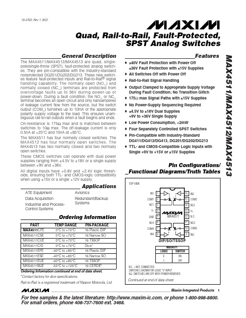
General DescriptionThe MAX4511/MAX4512/MAX4513 are quad, single-pole/single-throw (SPST), fault-protected analog switch-es. They are pin-compatible with the industry-standard nonprotected DG201/DG202/DG213. These new switch-es feature fault-protected inputs and Rail-to-Rail ®signal handling capability. The normally open (NO_) and normally closed (NC_) terminals are protected from overvoltage faults up to 36V during power-up or power-down. During a fault condition, the NO_ or NC_terminal becomes an open circuit and only nanoamperes of leakage current flow from the source, but the switch output (COM_) furnishes up to 10mA of the appropriate polarity supply voltage to the load. This ensures unam-biguous rail-to-rail outputs when a fault begins and ends.On-resistance is 175Ωmax and is matched between switches to 10Ωmax. The off-leakage current is only 0.5nA at +25°C and 10nA at +85°C.The MAX4511 has four normally closed switches. The MAX4512 has four normally open switches. The MAX4513 has two normally closed and two normally open switches.These CMOS switches can operate with dual power supplies ranging from ±4.5V to ±18V or a single supply between +9V and +36V.All digital inputs have +0.8V and +2.4V logic thresh-olds, ensuring both TTL- and CMOS-logic compatibility when using ±15V or a single +12V supply.ApplicationsFeatureso ±40V Fault Protection with Power Off±36V Fault Protection with ±15V Supplies o All Switches Off with Power Off o Rail-to-Rail Signal Handlingo Output Clamped to Appropriate Supply Voltage During Fault Condition; No Transition Glitch o 175Ωmax Signal Paths with ±15V Supplies o No Power-Supply Sequencing Required o ±4.5V to ±18V Dual Supplies +9V to +36V Single Supply o Low Power Consumption, <2mWo Four Separately Controlled SPST Switches o Pin-Compatible with Industry-StandardDG411/DG412/DG413, DG201/DG202/DG213o TTL- and CMOS-Compatible Logic Inputs with Single +9V to +15V or ±15V SuppliesFor free samples & the latest literature: , or phone 1-800-998-8800.For small orders, phone 408-737-7600 ext. 3468.MAX4511/MAX4512/MAX4513Quad, Rail-to-Rail, Fault-Protected,SPST Analog Switches________________________________________________________________Maxim Integrated Products119-4760; Rev 1; 8/02Ordering Information continued at end of data sheet.*Contact factory for dice specifications.Rail-to-Rail is a registered trademark of Nippon Motorola, Ltd.Ordering InformationPin Configurations/Functional Diagrams/Truth TablesATE Equipment Data Acquisition Industrial and Process-Control SystemsAvionicsRedundant/Backup SystemsM A X 4511/M A X 4512/M A X 4513Quad, Rail-to-Rail, Fault-Protected,SPST Analog Switches 2_______________________________________________________________________________________ABSOLUTE MAXIMUM RATINGSELECTRICAL CHARACTERISTICS—Dual Supplies(V+ = +15V, V- = -15V, GND = 0V, T A =T MIN to T MAX , unless otherwise noted. Typical values are at T A = +25°C.)Stresses beyond those listed under “Absolute Maximum Ratings” may cause permanent damage to the device. These are stress ratings only, and functional operation of the device at these or any other conditions beyond those indicated in the operational sections of the specifications is not implied. Exposure to absolute maximum rating conditions for extended periods may affect device reliability.Note 1:COM_ and IN_ pins are not fault protected. Signals on COM_ or IN_ exceeding V+ or V- are clamped by internal diodes.Limit forward diode current to maximum current rating.Note 2:NC_ and NO_ pins are fault protected. Signals on NC_ or NO_ exceeding -36V to +36V may damage the device. Theselimits apply with power applied to V+ or V-, or ±40V with V+ = V- = 0.(Voltages Referenced to GND)V+........................................................................-0.3V to +44.0V V-.........................................................................-44.0V to +0.3V V+ to V-................................................................-0.3V to +44.0V COM_, IN_ (Note 1)..............................(V- - 0.3V) to (V+ + 0.3V)NC_, NO_ (Note 2)..................................(V+ - 36V) to (V- + 36V)NC_, NO_ to COM_.................................................-36V to +36V Continuous Current into Any Terminal..............................±30mA Peak Current into Any Terminal(pulsed at 1ms, 10% duty cycle)...................................±50mAContinuous Power Dissipation (T A = +70°C) (Note 2)Plastic DIP (derate 10.53mW/°C above +70°C)...........842mW Narrow SO (derate 8.70mW/°C above +70°C).............696mW TSSOP (derate 9.4mW/°C above +70°C)..................754.7mW CERDIP (derate 10.00mW/°C above +70°C)................800mW Operating Temperature RangesMAX451_C_ E......................................................0°C to +70°C MAX451_E_ E...................................................-40°C to +85°C MAX451_MJE .................................................-55°C to +125°C Storage Temperature Range.............................-65°C to +150°C Lead Temperature (soldering, 10s).................................+300°CMAX4511/MAX4512/MAX4513Quad, Rail-to-Rail, Fault-Protected,SPST Analog Switches_______________________________________________________________________________________3ELECTRICAL CHARACTERISTICS—Dual Supplies (continued)(V+ = +15V, V- = -15V, GND = 0V, T A =T MIN to T MAX , unless otherwise noted. Typical values are at T A = +25°C.)M A X 4511/M A X 4512/M A X 4513Quad, Rail-to-Rail, Fault-Protected,SPST Analog Switches 4_______________________________________________________________________________________ELECTRICAL CHARACTERISTICS—Dual Supplies (continued)(V+ = +15V, V- = -15V, GND = 0V, T A = T MIN to T MAX , unless otherwise noted. Typical values are at T A = +25°C.)MAX4511/MAX4512/MAX4513Quad, Rail-to-Rail, Fault-Protected,SPST Analog Switches_______________________________________________________________________________________5ELECTRICAL CHARACTERISTICS—Single +12V Supply(V+ = +10.8V to +13.2V, V- = 0, T A = T MIN to T MAX , unless otherwise noted. Typical values are at T A = +25°C.)M A X 4511/M A X 4512/M A X 4513Quad, Rail-to-Rail, Fault-Protected,SPST Analog Switches 6_______________________________________________________________________________________Note 1:COM_ and IN_ pins are not fault protected. Signals on COM_ or IN_ exceeding V+ or V- are clamped by internal diodes.Limit forward diode current to maximum current rating.Note 2:NC_ and NO_ pins are fault protected. Signals on NC_ or NO_ exceeding -36V to +36V may damage the device. These limits apply with power applied to V+ or V-, or ±40V with V+ = V- = 0.Note 3:The algebraic convention is used in this data sheet; the most negative value is shown in the minimum column.Note 4:∆R ON = ∆R ON(MAX)- ∆R ON(MIN).Note 5:Leakage parameters are 100% tested at maximum rated hot temperature and guaranteed by correlation at T A = +25°C.Note 6:Guaranteed by design.Note 7:Off isolation = 20 log10 [ V COM_/ (V NC_or V NO_) ], V COM_= output, V NC_or V NO_= input to off switch.Note 8:Between any two switches.Note 9:Leakage testing for single-supply operation is guaranteed by testing with dual supplies.ELECTRICAL CHARACTERISTICS—Single +12V Supply (continued)(V+ = +10.8V to +13.2V, V- = 0, T A = T MIN to T MAX , unless otherwise noted. Typical values are at T A = +25°C.)MAX4511/MAX4512/MAX4513Quad, Rail-to-Rail, Fault-Protected,SPST Analog Switches_______________________________________________________________________________________7__________________________________________Typical Operating Characteristics(T A = +25°C, unless otherwise noted.)010050250200150300350-20-50-15-105101520SWITCH ON-RESISTANCE vs. V COM (DUAL SUPPLIES)V COM (V)S W I T C H O N -R E S I S T A N C E (Ω)80602040160140100120180200-15-50-1051015SWITCH ON-RESISTANCE vs. V COM AND TEMPERATURE (DUAL SUPPLIES)V COM (V)S W I T C H O N -R E S I S T A N C E (Ω)100010051015202530SWITCH ON-RESISTANCE vs. V COM (SINGLE SUPPLY)V COM (V)S W I T C H O N -R E S I S I T A N C E (Ω)050200150100300350250400046281012SWITCH ON-RESISTANCE vs. V COM AND TEMPERATURE (SINGLE SUPPLY)V COM (V)S W I T C H O N -R E S I S T A N C E (Ω)0300200100700800600500400900100005101520ON AND OFF TIMES vs. SUPPLY VOLTAGESUPPLY VOLTAGE (±V)t O N , t O F F (n s )1p10p100p1n10n 100n-50-25255075100125150I D(ON), I S(OFF), AND I D(OFF) LEAKAGES vs. TEMPERATURETEMPERATURE (°C)L E A K A G E (A )02810641214-15-10-5051015CHARGE INJECTION vs. V COM (DUAL SUPPLIES)V COM (V)Q (p C )010*******500400600-5025-255075100125ON AND OFF TIMES vs. TEMPERATURETEMPERATURE (°C)t O N , t O F F (n s )100300200500400600-50025-255075100125POWER-SUPPLY CURRENT vs. TEMPERATURETEMPERATURE (°C)S U P P L Y C U R R E N T (µA )M A X 4511/M A X 4512/M A X 4513Quad, Rail-to-Rail, Fault-Protected,SPST Analog Switches 8_______________________________________________________________________________________00.51.51.02.52.03.001015520253035LOGIC-LEVEL THRESHOLD vs. V+M A X 4511-10V+ (V)L O G I C -L E V E L T H R E S H O L D (V )Typical Operating Characteristics (continued)(T A = +25°C, unless otherwise noted.)0-10-20-1200.010.11101001000FREQUENCY RESPONSE-90-100-110FREQUENCY (MHz)L O S S (d B )P H A S E (D E G R E E S )-70-80-50-60-30-4012010080-120-60-80-100-20-402006040Pin Description*As long as the voltage on NO_ or NC_ does not exceed V+ or V-, NO_ (or NC_) and COM_ pins are identical and interchange-able. Either may be considered as an input or output; signals pass equally well in either direction.Detailed DescriptionOverview of Traditional Fault-Protected SwitchesThe MAX4511/MAX4512/MAX4513 are fault-protected CMOS analog switches with unusual operation and construction. Traditional fault-protected switches are constructed by three series FETs. This produces good off characteristics, but fairly high on-resistance when the signals are within about 3V of each supply rail. As the voltage on one side of the switch approaches with-in about 3V of either supply rail (a fault condition), the switch impedance becomes higher, limiting the output signal range (on the protected side of the switch) to approximately 3V less than the appropriate polarity supply voltage.During a fault condition, the output current that flows from the protected side of the switch into its load comes from the fault source on the other side of the switch. I f the switch is open or the load is extremely high impedance, the input current will be very low. I f the switch is on and the load is low impedance,enough current will flow from the source to maintain the load voltage at 3V less than the supply.MAX4511/MAX4512/MAX4513Quad, Rail-to-Rail, Fault-Protected,SPST Analog Switches_______________________________________________________________________________________9Overview of MAX4511/MAX4512/MAX4513The MAX4511/MAX4512/MAX4513 differ considerably from traditional fault-protection switches, with several advantages. First, they are constructed with two paral-lel FETs, allowing very low on-resistance when the switch is on. Second, they allow signals on the NC_ or NO_ pins that are within or slightly beyond the supply rails to be passed through the switch to the COM termi-nal, allowing rail-to-rail signal operation. Third, when a signal on NC_ or NO_ exceeds the supply rails by about 50mV (a fault condition), the voltage on COM_ is limited to the appropriate polarity supply voltage.Operation is identical for both fault polarities. The fault-protection extends to ±36V from GND.During a fault condition, the NO_ or NC_ input pin becomes high impedance regardless of the switch state or load resistance. If the switch is on, the COM_output current is furnished from the V+ or V- pin by “booster” FETs connected to each supply pin. These FETs can typically source or sink up to 10mA.When power is removed, the fault protection is still in effect. In this case, the NO_ or NC_ terminals are a vir-tual open circuit. The fault can be up to ±40V.The COM_ pins are not fault protected; they act as nor-mal CMOS switch pins. If a voltage source is connect-ed to any COM_ pin, it should be limited to the supply voltages. Exceeding the supply voltage will cause high currents to flow through the ESD protection diodes,possibly damaging the device (see Absolute Maximum Ratings ).Pin CompatibilityThese switches have identical pinouts to common non-fault-protected CMOS switches. Care should be exer-cised in considering them for direct replacements in existing printed circuit boards, however, since only the NO_ and NC_ pins of each switch are fault protected.Internal ConstructionInternal construction is shown in Figure 1, with the ana-log signal paths shown in bold. A single normally openFigure 1. Block DiagramM A X 4511/M A X 4512/M A X 4513Quad, Rail-to-Rail, Fault-Protected,SPST Analog Switches 10______________________________________________________________________________________(NO) switch is shown; the normally closed (NC) config-uration is identical except the logic-level translator becomes an inverter. The analog switch is formed by the parallel combination of N-channel FET N1 and P-channel FET P1, which are driven on and off simultane-ously according to the input fault condition and the logic-level state.Normal OperationTwo comparators continuously compare the voltage on the NO_ (or NC_) pin with V+ and V-. When the signal on NO_ or NC_ is between V+ and V- the switch acts normally, with FETs N1 and P1 turning on and off in response to I N_ signals. The parallel combination of N1 and P1 forms a low-value resistor between NO_ (or NC_) and COM_ so that signals pass equally well in either direction.Positive Fault ConditionWhen the signal on NO_ (or NC_) exceeds V+ by about 50mV, the high-fault comparator output is high, turning off FETs N1 and P1. This makes the NO_ (or NC_) pin high impedance regardless of the switch state. I f the switch state is “off”, all FETs are turned off and both NO_ (or NC_) and COM_ are high impedance. I f the switch state is “on”, FET P2 is turned on, sourcing cur-rent from V+ to COM_.Negative Fault ConditionWhen the signal on NO_ (or NC_) exceeds V- by about 50mV, the low-fault comparator output is high, turning off FETs N1 and P1. This makes the NO_ (or NC_) pin high impedance regardless of the switch state. I f the switch state is “off,” all FETs are turned off and both NO_ (or NC_) and COM_ are high impedance. I f the switch state is “on,” FET N2 is turned on, sinking cur-rent from COM_ to V-.Transient Fault Response and RecoveryWhen a fast rise-time and fall-time transient on I N_exceeds V+ or V-, the output (COM_) follows the input (I N_) to the supply rail with only a few nanoseconds delay. This delay is due to the switch on-resistance and circuit capacitance to ground. When the input transient returns to within the supply rails, however, there is a longer output recovery time delay. For positive faults, the recovery time is typically 3.5µs. For negative faults, the recovery time is typically 1.3µs. These values depend on the COM_ output resistance and capacitance, and are not production tested or guaranteed. The delays are not dependent on the fault amplitude. Higher COM_ output resistance and capacitance increase recovery times.COM_ and IN_ PinsFETs N2 and P2 can source about ±10mA from V+ or V-to the COM_ pin in the fault condition. Ensure that if the COM_ pin is connected to a low-resistance load, the absolute maximum current rating of 30mA is never exceeded, both in normal and fault conditions.The GND, COM_, and IN_ pins do not have fault protec-tion. Reverse ESD-protection diodes are internally con-nected between GND, COM_, IN_ and both V+ and V-. If a signal on GND, COM_, or I N_ exceeds V+ or V- by more than 300mV, one of these diodes will conduct heavily. During normal operation these reverse-biased ESD diodes leak a few nanoamps of current to V+ and V-.Fault-Protection Voltage and Power OffThe maximum fault voltage on the NC_ or NO_ pins is ±36V with power applied and ±40V with power off.Failure ModesThe MAX4511/MAX4512/MAX4513 are not lightning arrestors or surge protectors.Exceeding the fault-protection voltage limits on NO_ or NC_, even for very short periods, can cause the device to fail. The failure modes may not be obvious, and fail-ure in one switch may or may not affect other switches in the same package.GroundThere is no connection between the analog signal paths and GND. The analog signal paths consist of an N-channel and P-channel MOSFET with their sources and drains paralleled and their gates driven out of phase to V+ and V- by the logic-level translators.V+ and GND power the internal logic and logic-level translators and set the input logic thresholds. The logic-level translators convert the logic levels to switched V+and V- signals to drive the gates of the analog switch-es. This drive signal is the only connection between the power supplies and the analog signals. GND, IN_, and COM_ have ESD-protection diodes to V+ and V-.IN_ Logic-Level ThresholdsThe logic-level thresholds are CMOS and TTL compati-ble when V+ is +15V. As V+ is raised the threshold increases slightly, and when V+ reaches 25V the level threshold is about 2.8V—above the TTL output high level minimum of 2.4V, but still compatible with CMOS outputs (see Typical Operating Characteristics ).Increasing V- has no effect on the logic-level thresholds,but it does increase the gate-drive voltage to the signal FETs, reducing their on-resistance.MAX4511/MAX4512/MAX4513Quad, Rail-to-Rail, Fault-Protected,SPST Analog Switches______________________________________________________________________________________11Bipolar SuppliesThe MAX4511/MAX4512/MAX4513 operate with bipolar supplies between ±4.5V and ±18V. The V+ and V- sup-plies need not be symmetrical, but their difference can not exceed the absolute maximum rating of 44V.Single SupplyThe MAX4511/MAX4512/MAX4513 operate from a sin-gle supply between +9V and +36V when V- is connect-ed to GND.High-Frequency PerformanceIn 50Ωsystems, signal response is reasonably flat up to 50MHz (see Typical Operating Characteristics ). Above20MHz, the on-response has several minor peaks that are highly layout dependent. The problem with high-fre-quency operation is not turning the switch on, but turn-ing it off. The off-state switch acts like a capacitor and passes higher frequencies with less attenuation. At 10MHz, off isolation is about -42dB in 50Ωsystems,becoming worse (approximately 20dB per decade) as frequency increases. Higher circuit impedances also make off isolation worse. Adjacent channel attenuation is about 3dB above that of a bare IC socket and is due entirely to capacitive coupling.Figure 2. Switch Turn-On/Turn-Off TimesTest Circuits/Timing DiagramsFigure 3. MAX4513 Break-Before-Make IntervalM A X 4511/M A X 4512/M A X 4513Quad, Rail-to-Rail, Fault-Protected,SPST Analog Switches 12______________________________________________________________________________________Figure 4. Charge InjectionFigure 5. COM_, NO_, NC_ CapacitanceTest Circuits/Timing Diagrams (continued)MAX4511/MAX4512/MAX4513Quad, Rail-to-Rail, Fault-Protected,SPST Analog Switches______________________________________________________________________________________13Figure 6. Frequency Response, Off Isolation, and CrosstalkTest Circuits/Timing Diagrams (continued)Pin Configurations/Functional Diagrams/Truth Tables (continued)M A X 4511/M A X 4512/M A X 4513Quad, Rail-to-Rail, Fault-Protected,SPST Analog Switches 14______________________________________________________________________________________V-GNDNC4COM4IN4IN3COM30.086"(2.261mm)MAX4511NO1NO2COM1IN1IN2COM2COM4NO4IN4IN3NO3COM30.086"(2.261mm)MAX4512Ordering Information (continued)Chip TopographiesV-GNDCOM4NO4IN4IN3NC3COM3MAX45130.086"(2.261mm)TRANSISTOR COUNT: 139SUBSTRATE CONNECTED TO:V+*Contact factory for dice specifications.MAX4511/MAX4512/MAX4513Quad, Rail-to-Rail, Fault-Protected,SPST Analog Switches______________________________________________________________________________________15Package Information(The package drawing(s) in this data sheet may not reflect the most current specifications. For the latest package outline information,go to /packages .)M A X 4511/M A X 4512/M A X 4513Quad, Rail-to-Rail, Fault-Protected,SPST Analog Switches 16______________________________________________________________________________________Package Information (continued)(The package drawing(s) in this data sheet may not reflect the most current specifications. For the latest package outline information,go to /packages.)MAX4511/MAX4512/MAX4513Quad, Rail-to-Rail, Fault-Protected,SPST Analog SwitchesMaxim cannot assume responsibility for use of any circuitry other than circuitry entirely embodied in a Maxim product. No circuit patent licenses are implied. Maxim reserves the right to change the circuitry and specifications without notice at any time.Maxim Integrated Products, 120 San Gabriel Drive, Sunnyvale, CA 94086 408-737-7600______________________17©2002 Maxim Integrated ProductsPrinted USAis a registered trademark of Maxim Integrated Products.Package Information (continued)(The package drawing(s) in this data sheet may not reflect the most current specifications. For the latest package outline information,go to /packages .)。
MAX3222E中文材料
MAX3222E/MAX3232E/MAX3237E/MAX3241E/MAX3246E为+3.0V供电的EIA/TIA-232和V.28/V.24通信接口芯片,具有低功耗、高数据速率、增强型ESD保护等特性。
增强型ESD结构为所有发送器输出和接收器输入提供保护,可承受±15kV IEC 1000-4-2气隙放电、±8kV IEC 1000-4-2接触放电(MAX3246E为±9kV)和±15kV人体放电模式。
MAX3237E的逻辑引脚及接收器I/O引脚均提供上述保护,而它的发送器输出引脚提供±15kV人体放电模式的保护。
采用专有的低压差发送输出级,+3.0V至+5.5V供电时利用内部双电荷泵提供真正的RS-232性能。
工作于+3.3V电源时,荷泵仅需要四个0.1µF的小电容。
每款器件保证在250kbps数据速率下维持RS-232输出电平。
MAX3237E确保标准工作模式下提供250kbps的数据速率、在MegaBaud™工作模式下速率高达1Mbps。
MAX3222E/MAX3232E包括两个发送器和两个接收器;MAX3222E具有1µA关断模式,可降低电池供电便携式系统的功耗。
关断模式下,MAX3222E接收器仍保持有效状态,允许监视外设,而且仅消耗1µA的电源电流。
MAX3222E和MAX3232E的引脚、封装和功能分别兼容于工业标准的MAX242和MAX232。
MAX3241E/MAX3246E提供完备的串口(3个驱动器/5个接收器),专为笔记本电脑和亚笔记本电脑设计。
MAX3237E (5个驱动器/3个接收器)非常适合要求高速数据传输的外围设备。
这些器件都具有关断模式,此模式下所有接收器仍保持有效状态,而且仅消耗1µA (MAX3241E/MAX3246E)或10nA (MAX3237E)的电流。
MAX3222E、MAX3232E和MAX3241E都具有节省空间的SO、SSOP、TQFN及TSSOP封装,MAX3237E提供SSOP封装,MAX3246E提供超小型6 x 6 UCSP™封装。
MAX4211EEUE+中文资料
25:1
IOUT POUT
1.21V REFERENCE INHIBIT
REF
CIN1+
COUT1 CIN1LE CIN2+ COUT2
µMAX is a registered trademark of Maxim Integrated Products, Inc. Pin Configurations and Selector Guide appear at end of data sheet.
Stresses beyond those listed under “Absolute Maximum Ratings” may cause permanent damage to the device. These are stress ratings only, and functional operation of the device at these or any other conditions beyond those indicated in the operational sections of the specifications is not implied. Exposure to absolute maximum rating conditions for extended periods may affect device reliability.
Functional Diagrams
+
VSENSE RSENSE LOAD RS+ VCC 2.7V TO 5.5V RS-
-
Applications
Overpower Circuit Breakers Smart Battery Packs/Chargers Smart Peripheral Control Short-Circuit Protection Power-Supply Displays Measurement Instrumentation Baseband Analog Multipliers VGA Circuits Power-Level Detectors
MAX211ECWI+中文资料

________________________________________________________________Maxim Integrated Products 1General DescriptionThe MAX202E–MAX213E, MAX232E/MAX241E line drivers/receivers are designed for RS-232 and V.28communications in harsh environments. Each transmitter output and receiver input is protected against ±15kV electrostatic discharge (ESD) shocks, without latchup.The various combinations of features are outlined in the Selector Guide.The drivers and receivers for all ten devices meet all EIA/TIA-232E and CCITT V.28specifications at data rates up to 120kbps, when loaded in accordance with the EIA/TIA-232E specification.The MAX211E/MAX213E/MAX241E are available in 28-pin SO packages, as well as a 28-pin SSOP that uses 60% less board space. The MAX202E/MAX232E come in 16-pin TSSOP, narrow SO, wide SO, and DIP packages. The MAX203E comes in a 20-pin DIP/SO package, and needs no external charge-pump capacitors. The MAX205E comes in a 24-pin wide DIP package, and also eliminates external charge-pump capacitors. The MAX206E/MAX207E/MAX208E come in 24-pin SO, SSOP, and narrow DIP packages. The MAX232E/MAX241E operate with four 1µF capacitors,while the MAX202E/MAX206E/MAX207E/MAX208E/MAX211E/MAX213E operate with four 0.1µF capacitors,further reducing cost and board space.________________________ApplicationsNotebook, Subnotebook, and Palmtop Computers Battery-Powered Equipment Hand-Held EquipmentNext-Generation Device Featureso For Low-Voltage ApplicationsMAX3222E/MAX3232E/MAX3237E/MAX3241E/MAX3246E: ±15kV ESD-Protected Down to10nA, +3.0V to +5.5V, Up to 1Mbps, True RS-232Transceivers (MAX3246E Available in a UCSP™Package)o For Low-Power ApplicationsMAX3221/MAX3223/MAX3243: 1µA SupplyCurrent, True +3V to +5.5V RS-232 Transceivers with Auto-Shutdown™o For Space-Constrained ApplicationsMAX3233E/MAX3235E: ±15kV ESD-Protected,1µA, 250kbps, +3.0V/+5.5V, Dual RS-232Transceivers with Internal Capacitorso For Low-Voltage or Data Cable ApplicationsMAX3380E/MAX3381E: +2.35V to +5.5V, 1µA,2Tx/2Rx RS-232 Transceivers with ±15kV ESD-Protected I/O and Logic PinsMAX202E–MAX213E, MAX232E/MAX241E±15kV ESD-Protected, +5V RS-232 TransceiversSelector Guide19-0175; Rev 6; 3/05Pin Configurations and Typical Operating Circuits appear at end of data sheet.YesPARTNO. OF RS-232DRIVERSNO. OF RS-232RECEIVERSRECEIVERS ACTIVE IN SHUTDOWNNO. OF EXTERNAL CAPACITORS(µF)LOW-POWER SHUTDOWNTTL TRI-STATE MAX202E 220 4 (0.1)No No MAX203E 220None No No MAX205E 550None Yes Yes MAX206E 430 4 (0.1)Yes Yes MAX207E 530 4 (0.1)No No MAX208E 440 4 (0.1)No No MAX211E 450 4 (0.1)Yes Yes MAX213E 452 4 (0.1)Yes Yes MAX232E 220 4 (1)No No MAX241E454 (1)YesFor pricing, delivery, and ordering information,please contact Maxim/Dallas Direct!at 1-888-629-4642, or visit Maxim’s website at .AutoShutdown and UCSP are trademarks of Maxim Integrated Products, Inc.Ordering InformationOrdering Information continued at end of data sheet.2_______________________________________________________________________________________M A X 202E –M A X 213E , M A X 232E /M A X 241EABSOLUTE MAXIMUM RATINGSV CC ..........................................................................-0.3V to +6V V+................................................................(V CC - 0.3V) to +14V V-............................................................................-14V to +0.3V Input VoltagesT_IN............................................................-0.3V to (V+ + 0.3V)R_IN...................................................................................±30V Output VoltagesT_OUT.................................................(V- - 0.3V) to (V+ + 0.3V)R_OUT......................................................-0.3V to (V CC + 0.3V)Short-Circuit Duration, T_OUT....................................Continuous Continuous Power Dissipation (T A = +70°C)16-Pin Plastic DIP (derate 10.53mW/°C above +70°C)....842mW 16-Pin Narrow SO (derate 8.70mW/°C above +70°C).....696mW 16-Pin Wide SO (derate 9.52mW/°C above +70°C)......762mW 16-Pin TSSOP (derate 9.4mW/°C above +70°C)...........755mW20-Pin Plastic DIP (derate 11.11mW/°C above +70°C)...889mW 20-Pin SO (derate 10.00mW/°C above +70°C).............800mW 24-Pin Narrow Plastic DIP(derate 13.33mW/°C above +70°C) ...............................1.07W 24-Pin Wide Plastic DIP(derate 14.29mW/°C above +70°C)................................1.14W 24-Pin SO (derate 11.76mW/°C above +70°C).............941mW 24-Pin SSOP (derate 8.00mW/°C above +70°C)..........640mW 28-Pin SO (derate 12.50mW/°C above +70°C)....................1W 28-Pin SSOP (derate 9.52mW/°C above +70°C)..........762mW Operating Temperature RangesMAX2_ _EC_ _.....................................................0°C to +70°C MAX2_ _EE_ _...................................................-40°C to +85°C Storage Temperature Range.............................-65°C to +165°C Lead Temperature (soldering, 10s).................................+300°CELECTRICAL CHARACTERISTICS(V CC = +5V ±10% for MAX202E/206E/208E/211E/213E/232E/241E; V CC = +5V ±5% for MAX203E/205E/207E; C1–C4 = 0.1µF for MAX202E/206E/207E/208E/211E/213E; C1–C4 = 1µF for MAX232E/241E; T A = T MIN to T MAX ; unless otherwise noted. Typical values are at T A = +25°C.)Stresses beyond those listed under “Absolute Maximum Ratings” may cause permanent damage to the device. These are stress ratings only, and functional operation of the device at these or any other conditions beyond those indicated in the operational sections of the specifications is not implied. Exposure to absolute maximum rating conditions for extended periods may affect device reliability.ELECTRICAL CHARACTERISTICS (continued)MAX202E–MAX213E, MAX232E/MAX241E (V CC= +5V ±10% for MAX202E/206E/208E/211E/213E/232E/241E; V CC= +5V ±5% for MAX203E/205E/207E; C1–C4 = 0.1µF forMAX202E/206E/207E/208E/211E/213E; C1–C4 = 1µF for MAX232E/241E; T A= T MIN to T MAX; unless otherwise noted. Typical valuesare at T A= +25°C.)Note 1:MAX211EE_ _ tested with V CC= +5V ±5%._______________________________________________________________________________________34______________________________________________________________________________________M A X 202E –M A X 213E , M A X 232E /M A X 241E__________________________________________Typical Operating Characteristics(Typical Operating Circuits, V CC = +5V, T A = +25°C, unless otherwise noted.)5.00MAX211E/MAX213ETRANSMITTER OUTPUT VOLTAGEvs. LOAD CAPACITANCELOAD CAPACITANCE (pF)V O H , -V O L (V )5.56.06.57.07.58.0100020003000400050000MAX211E/MAX213E/MAX241E TRANSMITTER SLEW RATE vs. LOAD CAPACITANCELOAD CAPACITANCE (pF)S L E W R A T E ( V /µs )5101520253010002000300040005000_______________________________________________________________________________________5MAX202E–MAX213E, MAX232E/MAX241E____________________________Typical Operating Characteristics (continued)(Typical Operating Circuits, V CC = +5V, T A = +25°C, unless otherwise noted.)2MAX202E/MAX203E/MAX232E TRANSMITTER SLEW RATE vs. LOAD CAPACITANCELOAD CAPACITANCE (pF)S L E W R A T E ( V /µs )468101214100020003000400050005.07.5-7.53000MAX205E–MAX208ETRANSMITTER OUTPUT VOLTAGEvs. LOAD CAPACITANCE-5.02.5LOAD CAPACITANCE (pF)O U T P U T V O L T A G E (V )10002000400050000-2.54550203000MAX205E–MAX208E SUPPLY CURRENT vs. LOAD CAPACITANCE2540LOAD CAPACITANCE (pF)S U P P L Y C U R R E N T (m A )100020004000500035302.55.0-10.0180MAX205E –MAX208EOUTPUT VOLTAGE vs. DATA RATE-7.50DATA RATE (kbps)O U T P U T V O L T A G E (V )601202401503090210-2.5-5.010.07.56_______________________________________________________________________________________M A X 202E –M A X 213E , M A X 232E /M A X 241EMAX203EMAX205E_____________________________________________________________Pin DescriptionsMAX202E/MAX232E_______________________________________________________________________________________7MAX202E–MAX213E, MAX232E/MAX241EMAX208E________________________________________________Pin Descriptions (continued)MAX206EMAX207E8_______________________________________________________________________________________M A X 202E –M A X 213E , M A X 232E /M A X 241EMAX211E/MAX213E/MAX241E)(MAX205E/MAX206E/MAX211E/MAX213E/MAX241E)________________________________________________Pin Descriptions (continued)MAX211E/MAX213E/MAX241EFigure 3. Transition Slew-Rate Circuit_______________Detailed Description The MAX202E–MAX213E, MAX232E/MAX241E consist of three sections: charge-pump voltage converters, drivers (transmitters), and receivers. These E versions provide extra protection against ESD. They survive ±15kV discharges to the RS-232 inputs and outputs, tested using the Human Body Model. When tested according to IEC1000-4-2, they survive ±8kV contact-discharges and ±15kV air-gap discharges. The rugged E versions are intended for use in harsh environments or applications where the RS-232 connection is frequently changed (such as notebook computers). The standard (non-“E”) MAX202, MAX203, MAX205–MAX208, MAX211, MAX213, MAX232, and MAX241 are recommended for applications where cost is critical.+5V to ±10V Dual Charge-PumpVoltage Converter The +5V to ±10V conversion is performed by dual charge-pump voltage converters (Figure 4). The first charge-pump converter uses capacitor C1 to double the +5V into +10V, storing the +10V on the output filter capacitor, C3. The second uses C2 to invert the +10V into -10V, storing the -10V on the V- output filter capacitor, C4.In shutdown mode, V+ is internally connected to V CC by a 1kΩpull-down resistor, and V- is internally connected to ground by a 1kΩpull up resistor.RS-232 Drivers With V CC= 5V, the typical driver output voltage swing is ±8V when loaded with a nominal 5kΩRS-232 receiver. The output swing is guaranteed to meet EIA/TIA-232E and V.28 specifications that call for ±5V minimum output levels under worst-case conditions. These include a 3kΩload, minimum V CC, and maximum operating temperature. The open-circuit output voltage swings from (V+ - 0.6V) to V-.Input thresholds are CMOS/TTL compatible. The unused drivers’ inputs on the MAX205E–MAX208E, MAX211E, MAX213E, and MAX241E can be left unconnected because 400kΩpull up resistors to V CC are included on-chip. Since all drivers invert, the pull up resistors force the unused drivers’ outputs low. The MAX202E, MAX203E, and MAX232E do not have pull up resistors on the transmitter inputs._______________________________________________________________________________________9MAX202E–MAX213E, MAX232E/MAX241E10______________________________________________________________________________________M A X 202E –M A X 213E , M A X 232E /M A X 241E±15kV ESD-Protected, +5V RS-232 Transceivers When in low-power shutdown mode, the MAX205E/MAX206E/MAX211E/MAX213E/MAX241E driver outputs are turned off and draw only leakage currents—even if they are back-driven with voltages between 0V and 12V. Below -0.5V in shutdown, the transmitter output is diode-clamped to ground with a 1k Ωseries impedance.RS-232 ReceiversThe receivers convert the RS-232 signals to CMOS-logic output levels. The guaranteed 0.8V and 2.4V receiver input thresholds are significantly tighter than the ±3V thresholds required by the EIA/TIA-232E specification.This allows the receiver inputs to respond to TTL/CMOS-logic levels, as well as RS-232 levels.The guaranteed 0.8V input low threshold ensures that receivers shorted to ground have a logic 1 output. The 5k Ωinput resistance to ground ensures that a receiver with its input left open will also have a logic 1 output. Receiver inputs have approximately 0.5V hysteresis.This provides clean output transitions, even with slow rise/fall-time signals with moderate amounts of noise and ringing.In shutdown, the MAX213E’s R4 and R5 receivers have no hysteresis.Shutdown and Enable Control (MAX205E/MAX206E/MAX211E/MAX213E/MAX241E)In shutdown mode, the charge pumps are turned off,V+ is pulled down to V CC , V- is pulled to ground, and the transmitter outputs are disabled. This reduces supply current typically to 1µA (15µA for the MAX213E).The time required to exit shutdown is under 1ms, as shown in Figure 5.ReceiversAll MAX213E receivers, except R4 and R5, are put into a high-impedance state in shutdown mode (see Tables 1a and 1b). The MAX213E’s R4 and R5 receivers still function in shutdown mode. These two awake-in-shutdown receivers can monitor external activity while maintaining minimal power consumption.The enable control is used to put the receiver outputs into a high-impedance state, to allow wire-OR connection of two EIA/TIA-232E ports (or ports of different types) at the UART. It has no effect on the RS-232 drivers or the charge pumps.N ote: The enabl e control pin is active l ow for the MAX211E/MAX241E (EN ), but is active high for the MAX213E (EN). The shutdown control pin is active high for the MAX205E/MAX206E/MAX211E/MAX241E (SHDN), but is active low for the MAX213E (SHDN ).Figure 4. Charge-Pump DiagramMAX202E–MAX213E, MAX232E/MAX241EV+V-200µs/div3V 0V 10V 5V 0V -5V -10VSHDNMAX211EFigure 5. MAX211E V+ and V- when Exiting Shutdown (0.1µF capacitors)X = Don't care.*Active = active with reduced performanceSHDN E N OPERATION STATUS Tx Rx 00Normal Operation All Active All Active 01Normal Operation All Active All High-Z 1XShutdownAll High-ZAll High-ZTable 1a. MAX205E/MAX206E/MAX211E/MAX241E Control Pin ConfigurationsTable 1b. MAX213E Control Pin ConfigurationsThe MAX213E’s receiver propagation delay is typically 0.5µs in normal operation. In shutdown mode,propagation delay increases to 4µs for both rising and falling transitions. The MAX213E’s receiver inputs have approximately 0.5V hysteresis, except in shutdown,when receivers R4 and R5 have no hysteresis.When entering shutdown with receivers active, R4 and R5 are not valid until 80µs after SHDN is driven low.When coming out of shutdown, all receiver outputs are invalid until the charge pumps reach nominal voltage levels (less than 2ms when using 0.1µF capacitors).±15kV ESD ProtectionAs with all Maxim devices, ESD-protection structures are incorporated on all pins to protect against electrostatic discharges encountered during handling and assembly. The driver outputs and receiver inputs have extra protection against static electricity. Maxim’s engineers developed state-of-the-art structures to protect these pins against ESD of ±15kV without damage. The ESD structures withstand high ESD in all states: normal operation, shutdown, and powered down. After an ESD event, Maxim’s E versions keep working without latchup, whereas competing RS-232products can latch and must be powered down to remove latchup.ESD protection can be tested in various ways; the transmitter outputs and receiver inputs of this product family are characterized for protection to the following limits:1)±15kV using the Human Body Model2)±8kV using the contact-discharge method specifiedin IEC1000-4-23)±15kV using IEC1000-4-2’s air-gap method.ESD Test ConditionsESD performance depends on a variety of conditions.Contact Maxim for a reliability report that documents test set-up, test methodology, and test results.Human Body ModelFigure 6a shows the Human Body Model, and Figure 6b shows the current waveform it generates when discharged into a low impedance. This model consists of a 100pF capacitor charged to the ESD voltage of interest, which is then discharged into the test device through a 1.5k Ωresistor.S H D N ENOPERATION STATUS Tx 1–400Shutdown All High-Z 01Shutdown All High-Z 10Normal Operation 11Normal OperationAll ActiveAll Active Active1–34, 5High-Z ActiveHigh-Z High-Z High-Z Active*High-Z RxM A X 202E –M A X 213E , M A X 232E /M A X 241EIEC1000-4-2The IEC1000-4-2 standard covers ESD testing and performance of finished equipment; it does not specifically refer to integrated circuits. The MAX202E/MAX203E–MAX213E, MAX232E/MAX241E help you design equipment that meets level 4 (the highest level) of IEC1000-4-2, without the need for additional ESD-protection components.The major difference between tests done using the Human Body Model and IEC1000-4-2 is higher peak current in IEC1000-4-2, because series resistance is lower in the IEC1000-4-2 model. Hence, the ESD withstand voltage measured to IEC1000-4-2 is generally lower than that measured using the Human Body Model. Figure 7b shows the current waveform for the 8kV IEC1000-4-2 level-four ESD contact-discharge test.The air-gap test involves approaching the device with a charged probe. The contact-discharge method connects the probe to the device before the probe is energized.Machine ModelThe Machine Model for ESD tests all pins using a 200pF storage capacitor and zero discharge resistance. Its objective is to emulate the stress caused by contact that occurs with handling and assembly during manufacturing. Of course, all pins require this protection during manufacturing, not just RS-232 inputs and outputs. Therefore,after PC board assembly,theMachine Model is less relevant to I/O ports.Figure 7a. IEC1000-4-2 ESD Test ModelFigure 7b. IEC1000-4-2 ESD Generator Current WaveformFigure 6a. Human Body ESD Test ModelFigure 6b. Human Body Model Current Waveform__________Applications InformationCapacitor Selection The capacitor type used for C1–C4 is not critical for proper operation. The MAX202E, MAX206–MAX208E, MAX211E, and MAX213E require 0.1µF capacitors, and the MAX232E and MAX241E require 1µF capacitors, although in all cases capacitors up to 10µF can be used without harm. Ceramic, aluminum-electrolytic, or tantalum capacitors are suggested for the 1µF capacitors, and ceramic dielectrics are suggested for the 0.1µF capacitors. When using the minimum recommended capacitor values, make sure the capacitance value does not degrade excessively as the operating temperature varies. If in doubt, use capacitors with a larger (e.g., 2x) nominal value. The capacitors’ effective series resistance (ESR), which usually rises at low temperatures, influences the amount of ripple on V+ and V-.Use larger capacitors (up to 10µF) to reduce the output impedance at V+ and V-. This can be useful when “stealing” power from V+ or from V-. The MAX203E and MAX205E have internal charge-pump capacitors. Bypass V CC to ground with at least 0.1µF. In applications sensitive to power-supply noise generated by the charge pumps, decouple V CC to ground with a capacitor the same size as (or larger than) the charge-pump capacitors (C1–C4).V+ and V- as Power Supplies A small amount of power can be drawn from V+ and V-, although this will reduce both driver output swing and noise margins. Increasing the value of the charge-pump capacitors (up to 10µF) helps maintain performance when power is drawn from V+ or V-.Driving Multiple Receivers Each transmitter is designed to drive a single receiver. Transmitters can be paralleled to drive multiple receivers.Driver Outputs when Exiting Shutdown The driver outputs display no ringing or undesirable transients as they come out of shutdown.High Data Rates These transceivers maintain the RS-232 ±5.0V minimum driver output voltages at data rates of over 120kbps. For data rates above 120kbps, refer to the Transmitter Output Voltage vs. Load Capacitance graphs in the Typical Operating Characteristics. Communication at these high rates is easier if the capacitive loads on the transmitters are small; i.e., short cables are best.Table 2. Summary of EIA/TIA-232E, V.28 SpecificationsMAX202E–MAX213E, MAX232E/MAX241EM A X 202E –M A X 213E , M A X 232E /M A X 241E____________Pin Configurations and Typical Operating Circuits (continued)Table 3. DB9 Cable ConnectionsCommonly Used for EIA/TIAE-232E and V.24 Asynchronous Interfaces____________Pin Configurations and Typical Operating Circuits (continued)MAX202E–MAX213E, MAX232E/MAX241EM A X 202E –M A X 213E , M A X 232E /M A X 241E____________Pin Configurations and Typical Operating Circuits (continued)MAX202E–MAX213E, MAX232E/MAX241E____________Pin Configurations and Typical Operating Circuits (continued)M A X 202E –M A X 213E , M A X 232E /M A X 241E____________Pin Configurations and Typical Operating Circuits (continued)MAX202E–MAX213E, MAX232E/MAX241E____________Pin Configurations and Typical Operating Circuits (continued)M A X 202E –M A X 213E , M A X 232E /M A X 241E____________Pin Configurations and Typical Operating Circuits (continued)______________________________________________________________________________________21MAX202E–MAX213E, MAX232E/MAX241E Ordering Information (continued)*Dice are specified at T A= +25°C.M A X 202E –M A X 213E , M A X 232E /M A X 241E22________________________________________________________________________________________________________________________________________________Chip Topographies___________________Chip InformationC1-V+C1+V CC R2INT2OUT R2OUT0.117"(2.972mm)0.080"(2.032mm)V-C2+ C2-T2IN T1OUT R1INR1OUT T1INGNDR5INV-C2-C2+C1-V+C1+V CC T4OUTR3IN T3OUTT1OUT 0.174"(4.420mm)0.188"(4.775mm)T4IN R5OUT R4OUT T3IN R4IN EN (EN) SHDN (SHDN)R3OUT T2OUT GNDR1IN R1OUT T2IN R2OUTR2IN T1IN ( ) ARE FOR MAX213E ONLYTRANSISTOR COUNT: 123SUBSTRATE CONNECTED TO GNDTRANSISTOR COUNT: 542SUBSTRATE CONNECTED TO GNDMAX202E/MAX232EMAX211E/MAX213E/MAX241EMAX205E/MAX206E/MAX207E/MAX208E TRANSISTOR COUNT: 328SUBSTRATE CONNECTED TO GNDMAX202E–MAX213E, MAX232E/MAX241E Package InformationM A X 202E –M A X 213E , M A X 232E /M A X 241EPackage Information (continued)MAX202E–MAX213E, MAX232E/MAX241E±15kV ESD-Protected, +5V RS-232 TransceiversMaxim cannot assume responsibility for use of any circuitry other than circuitry entirely embodied in a Maxim product. No circuit patent licenses are implied. Maxim reserves the right to change the circuitry and specifications without notice at any time.Maxim Integrated Products, 120 San Gabriel Drive, Sunnyvale, CA 94086 408-737-7600 ____________________25©2005 Maxim Integrated ProductsPrinted USAis a registered trademark of Maxim Integrated Products, Inc.Package Information (continued)(The package drawing(s) in this data sheet may not reflect the most current specifications. For the latest package outline information go to /packages .)。
MAX262中文资料
M A X262中文资料(总5页) -CAL-FENGHAI.-(YICAI)-Company One1-CAL-本页仅作为文档封面,使用请直接删除在电子电路中,滤波器是不可或缺的部分,其中有源滤波器更为常用。
一般有源滤波器由运算放大器和RC元件组成,对元器件的参数精度要求比较高,设计和调试也比较麻烦。
美国Maxim公司生产的可编程滤波器芯片MAX262可以通过编程对各种低频信号实现低通、高通、带通、带阻以及全通滤波处理,且滤波的特性参数如中心频率、品质因数等,可通过编程进行设置,电路的外围器件也少。
本文介绍MAX262的情况以及由它构成的程控滤波器电路。
1 MAX262芯片介绍MAX262芯片是Maxim公司推出的双二阶通用开关电容有源滤波器,可通过微处理器精确控制滤波器的传递函数(包括设置中心频率、品质因数和工作方式)。
它采用CMOS工艺制造,在不需外部元件的情况下就可以构成各种带通、低通、高通、陷波和全通滤波器。
图1是它的引脚排列情况。
图1 MAX262引脚V+ ——正电源输入端。
V- ——负电源输入端。
GND ——模拟地。
CLKA ——外接晶体振荡器和滤波器A 部分的时钟输入端,在滤波器内部,时钟频率被2分频。
CLKB ——滤波器B 部分的时钟输入端,同样在滤波器内部,时钟频率被2分频。
CLKOUT ——晶体振荡器和R-C振荡的时钟输出端。
OSCOUT ——与晶体振荡器或R-C振荡器相连,用于自同步。
INA、INB ——滤波器的信号输入端。
BPA、BPB——带通滤波器输出端。
LPA、LPB——低通滤波器输出端。
HPA、HPB——高通、带阻、全通滤波器输出端。
WR ——写入有效输入端。
接V+时,输人数据不起作用;接V-时,数据可通过逻辑接口进入一个可编程的内存之中,以完成滤波器的工作模式、f0及Q的设置。
此外,还可以接收TTL电平信号,并上升沿锁存输人数据。
A0、A1、A2、A3 ——地址输人端,可用来完成对滤波器工作模式、f0和Q的相应设置。
MAX1228BCEP+;MAX1228BEEP+;MAX1230BEEG+;MAX1230BETI+;MAX1230BCEG+;中文规格书,Datasheet资料

o Accuracy: ±1 LSB INL, ±1 LSB DNL, No Missing Codes Over Temperature
o Scan Mode, Internal Averaging, and Internal Clock o Low-Power Single +5V Operation
(derate 20.8mW/°C above +70°C) ........................1667mW
Operating Temperature Ranges MAX12__C__.......................................................0°C to +70°C MAX12__E__ ....................................................-40°C to +85°C
Offset Error Gain Error
(Note 2)
MAX1986ETE中文资料

MAX1984/MAX1985/MAX1986
The MAX1984/MAX1985/MAX1986 are white light-emitting diode (LED) drivers that use individual regulators to control the current of up to eight LEDs. A high-efficiency step-up regulator generates just enough voltage to keep all the current regulators in regulation. A versatile dimming interface accommodates analog, digitally adjusted pulse-width modulation (DPWM), or parallel control. The individual current regulators allow good current matching between LEDs. Open or shorted LEDs cannot affect the performance of other LEDs. The step-up regulator achieves high efficiency by using synchronous rectification. The internal N-channel switch and P-channel synchronous rectifier eliminate the need for external MOSFETs and diodes. The 1MHz switching frequency allows the use of low-profile inductors and ceramic capacitors. The brightness can be easily adjusted using a multimode dimming interface, which allows brightness control through a DPWM signal, a 2- or 3-bit parallel control interface, or an analog signal. The DPWM signal can be connected directly to the control pin without the need for an external RC filter if its frequency is 10kHz or above. The MAX1984 drives up to eight LEDs, the MAX1985 drives up to six LEDs, and the MAX1986 drives up to four LEDs. Each device has an LED select pin (SEL) that allows one subset, the other subset, or all LEDs to be illuminated. All three devices are available in a 4mm ✕ 4mm thin QFN package.
MAX3232EEAE中文资料

MAX3222EEPN -40°C to +85°C 18 Plastic DIP —
MAX3232ECAE 0°C to +70°C 16 SSOP
—
MAX3232ECWE 0°C to +70°C 16 Wide SO —
MAX3232ECPE 0°C to +70°C 16 Plastic DIP —
General Description
The MAX3222E/MAX3232E/MAX3237E/MAX3241E/ MAX3246E +3.0V-powered EIA/TIA-232 and V.28/V.24 communications interface devices feature low power consumption, high data-rate capabilities, and enhanced electrostatic-discharge (ESD) protection. The enhanced ESD structure protects all transmitter outputs and receiver inputs to ±15kV using IEC 1000-4-2 Air-Gap Discharge, ±8kV using IEC 1000-4-2 Contact Discharge (±9kV for MAX3246E), and ±15kV using the Human Body Model. The logic and receiver I/O pins of the MAX3237E are protected to the above standards, while the transmitter output pins are protected to ±15kV using the Human Body Model.
- 1、下载文档前请自行甄别文档内容的完整性,平台不提供额外的编辑、内容补充、找答案等附加服务。
- 2、"仅部分预览"的文档,不可在线预览部分如存在完整性等问题,可反馈申请退款(可完整预览的文档不适用该条件!)。
- 3、如文档侵犯您的权益,请联系客服反馈,我们会尽快为您处理(人工客服工作时间:9:00-18:30)。
D0/D8 9 INT 10 RD 11 WR 12
0°C to +70°C -40°C to +85°C 28 QSOP -40°C to +85°C 28 QSOP
QSOP
Pin Configurations continued at end of data sheet. Typical Operating Circuits appear at end of data sheet.
Features
MAX1262/MAX1264
Pin Configurations
TOP VIEW
HBEN 1 D7 2 24 VLOGIC 23 VDD 22 REF 21 REFADJ 20 GND
Applications
Industrial Control Systems Energy Management Data-Acquisition Systems Data Logging Patient Monitoring Touch Screens
ELECTRICAL CHARACTERISTICS
(VDD = VLOGIC = +5V ±10%, COM = GND, REFADJ = VDD, VREF = +2.5V, 4.7µF capacitor at REF pin, fCLK = 7.6MHz (50% duty cycle), TA = TMIN to TMAX, unless otherwise noted. Typical values are at TA = +25°C.) PARAMETER DC ACCURACY (Note 1) Resolution Relative Accuracy (Note 2) Differential Nonlinearity Offset Error Gain Error Gain Temperature Coefficient Channel-to-Channel Offset Matching Signal-to-Noise Plus Distortion Total Harmonic Distortion (Including 5th-Order Harmonic) Spurious-Free Dynamic Range Intermodulation Distortion Channel-to-Channel Crosstalk Full-Linear Bandwidth Full-Power Bandwidth CONVERSION RATE External clock mode Conversion Time (Note 5) T/H Acquisition Time Aperture Delay Aperture Jitter External Clock Frequency Duty Cycle 2 fCLK tCONV tACQ External acquisition or external clock mode External acquisition or external clock mode Internal acquisition/internal clock mode 0.1 30 25 <50 <200 7.6 70 External acquisition/internal clock mode Internal acquisition/internal clock mode 2.1 2.5 3.2 3.0 3.6 3.5 4 400 ns ns ps MHz % µs SINAD THD SFDR IMD fIN1 = 49kHz, fIN2 = 52kHz fIN = 175kHz, VIN = 2.5VP-P (Note 4) SINAD > 68dB -3dB rolloff 80 76 -78 350 6 67 (Note 3) ±2 ±0.2 RES INL DNL MAX126_A MAX126_B No missing codes over temperature 12 ±0.5 ±1 ±1 ±4 ±4 Bits LSB LSB LSB LSB ppm/°C LSB SYMBOL CONDITIONS MIN TYP MAX UNITS
General Description
The MAX1262/MAX1264 low-power, 12-bit analog-todigital converters (ADCs) feature a successive-approximation ADC, automatic power-down, fast wake-up (2µs), an on-chip clock, +2.5V internal reference, and a high-speed, byte-wide parallel interface. The devices operate with a single +5V analog supply and feature a VLOGIC pin that allows them to interface directly with a +2.7V to +5.5V digital supply. Power consumption is only 10mW (VDD = VLOGIC) at a 400ksps max sampling rate. Two software-selectable power-down modes enable the MAX1262/MAX1264 to be shut down between conversions; accessing the parallel interface returns them to normal operation. Powering down between conversions can cut supply current to under 10µA at reduced sampling rates. Both devices offer software-configurable analog inputs for unipolar/bipolar and single-ended/pseudo-differential operation. In single-ended mode, the MAX1262 has eight input channels and the MAX1264 has four input channels (four and two input channels, respectively, when in pseudo-differential mode). Excellent dynamic performance and low power, combined with ease of use and small package size, make these converters ideal for battery-powered and dataacquisition applications or for other circuits with demanding power consumption and space requirements. The MAX1262 is available in a 28-pin QSOP package, while the MAX1264 comes in a 24-pin QSOP. For pincompatible +3V, 12-bit versions, refer to the MAX1261/ MAX1263 data sheet. o 12-Bit Resolution, ±0.5 LSB Linearity o +5V Single-Supply Operation o User-Adjustable Logic Level (+2.7V to +5.5V) o Internal +2.5V Reference o Software-Configurable Analog Input Multiplexer 8-Channel Single Ended/ 4-Channel Pseudo-Differential (MAX1262) 4-Channel Single Ended/ 2-Channel Pseudo-Differential (MAX1264) o Software-Configurable Unipolar/Bipolar Analog Inputs o Low Current 2.5mA (400ksps) 1.0mA (100ksps) 400µA (10ksps) 2µA (Shutdown) o Internal 6MHz Full-Power Bandwidth Track/Hold o Byte-Wide Parallel (8 + 4) Interface o Small Footprint 28-Pin QSOP (MAX1262) 24-Pin QSOP (MAX1264)
Ordering Information continued at end of data sheet.
________________________________________________________________ Maxim Integrated Products
1
For pricing, delivery, and ing information, please contact Maxim/Dallas Direct! at 1-888-629-4642, or visit Maxim’s website at .
元器件交易网
400ksps, +5V, 8-/4-Channel, 12-Bit ADCs with +2.5V Reference and Parallel Interface MAX1262/MAX1264