TLOE53TF中文资料
TEFD4300F;中文规格书,Datasheet资料

Silicon PIN PhotodiodeDESCRIPTIONTEF D4300F is a silicon PIN photodiode with high radiant sensitivity in black, T-1 plastic package with daylight blocking filter. Filter bandwitdth is matched with 850 nm to 950 nm IR emitters.FEATURES•Package type: leaded •Package form: T-1•Dimensions (in mm): Ø 3•High radiant sensitivity•Daylight blocking filter matched with 850 nm to 950 nm emitters •Fast response times•Angle of half sensitivity: ϕ = ± 20°•Package matched with IR emitter series VSLB3940,TSUS4300, and TSAL4400•Compliant to RoHS Directive 2002/95/EC and in accordance to WEEE 2002/96/ECNote**Please see document “Vishay Material Category Policy”:/doc?99902APPLICATIONS•High speed photo detector for data transmission •Optical switches •Counters and sorters •Interrupters •Encoders •Position sensorsNote•Test condition see table “Basic Characteristics”Note•MOQ: minimum order quantityPRODUCT SUMMARYCOMPONENT I ra (μA)ϕ (deg)λ0.5 (nm)TEFD4300F17± 20770 to 1070ORDERING INFORMATIONORDERING CODE PACKAGINGREMARKSPACKAGE FORMTEFD4300FBulkMOQ: 5000 pcs, 5000 pcs/bulkT-1ABSOLUTE MAXIMUM RATINGS (T amb = 25 °C, unless otherwise specified)PARAMETER TEST CONDITIONSYMBOLVALUE UNIT Reverse voltage V R 60V Power dissipation T amb ≤ 25 °C P V 215mW Junction temperature T j 100°C Operating temperature range T amb - 40 to + 100°C Storage temperature range T stg - 40 to + 100°C Soldering temperaturet ≤ 3 s, 2 mm from case T sd 260°C Thermal resistance junction/ambientConnected with Cu wire, 0.14 mm 2R thJA450K/WBASIC CHARACTERISTICS (T amb = 25 °C, unless otherwise specified)Fig. 1 - Reverse Dark Current vs. Ambient TemperatureFig. 2 - Relative Reverse Light Current vs. Ambient TemperatureBASIC CHARACTERISTICS (T amb = 25 °C, unless otherwise specified)PARAMETER TEST CONDITIONSYMBOLMIN.TYP.MAX.UNIT Forward voltage I F = 50 mA V F1V Breakdown voltage I R = 100 μA, E = 0 V (BR) 60V Reverse dark current V R = 10 V, E = 0 I ro 0.153nADiode capacitance V R = 0 V, f = 1 MHz, E = 0 C D 3.3p F V R = 5 V, f = 1 MHz, E = 0 C D 1.2pF Open circuit voltage E e = 1 mW/cm 2, λ = 950 nm V OC 350mV Temperature coefficient of V O E e = 1 mW/cm 2, λ = 950 nm TK Vo- 2.6mV/K Short circuit current E e = 1 mW/cm 2, λ = 950 nm I k 15μA Temperature coefficient of I k E e = 1 mW/cm 2, λ = 950 nmTK Ik 0.1%/KReverse light current E e = 1 mW/cm 2, λ = 950 nm, V R= 5 VI ra 91727μA Angle of half sensitivity ϕ± 20deg Wavelength of peak sensitivity λp 950nmRange of spectral bandwidth λ0.57701070nm Rise time V R = 10 V, R L = 1 k Ω, λ = 820 nm t r 100ns Fall timeV R = 10 V, R L = 1 k Ω, λ = 820 nmt f 100nsFig. 3 - Reverse Light Current vs. IrradianceFig. 4 - Diode Capacitance vs. Reverse Voltage Fig. 5 - Relative Spectral Sensitivity vs. Wavelength Fig. 6 - Relative Radiant Intensity vs. Angular Displacement Fig. 7 - Dark Current vs. Reverse VoltagePACKAGE DIMENSIONS in millimetersLegal Disclaimer Notice VishayDisclaimerALL PRODU CT, PRODU CT SPECIFICATIONS AND DATA ARE SU BJECT TO CHANGE WITHOU T NOTICE TO IMPROVE RELIABILITY, FUNCTION OR DESIGN OR OTHERWISE.Vishay Intertechnology, Inc., its affiliates, agents, and employees, and all persons acting on its or their behalf (collectively,“Vishay”), disclaim any and all liability for any errors, inaccuracies or incompleteness contained in any datasheet or in any other disclosure relating to any product.Vishay makes no warranty, representation or guarantee regarding the suitability of the products for any particular purpose or the continuing production of any product. To the maximum extent permitted by applicable law, Vishay disclaims (i) any and all liability arising out of the application or use of any product, (ii) any and all liability, including without limitation special, consequential or incidental damages, and (iii) any and all implied warranties, including warranties of fitness for particular purpose, non-infringement and merchantability.Statements regarding the suitability of products for certain types of applications are based on Vishay’s knowledge of typical requirements that are often placed on Vishay products in generic applications. Such statements are not binding statements about the suitability of products for a particular application. It is the customer’s responsibility to validate that a particular product with the properties described in the product specification is suitable for use in a particular application. Parameters provided in datasheets and/or specifications may vary in different applications and performance may vary over time. All operating parameters, including typical parameters, must be validated for each customer application by the customer’s technical experts. Product specifications do not expand or otherwise modify Vishay’s terms and conditions of purchase, including but not limited to the warranty expressed therein.Except as expressly indicated in writing, Vishay products are not designed for use in medical, life-saving, or life-sustaining applications or for any other application in which the failure of the Vishay product could result in personal injury or death. Customers using or selling Vishay products not expressly indicated for use in such applications do so at their own risk and agree to fully indemnify and hold Vishay and its distributors harmless from and against any and all claims, liabilities, expenses and damages arising or resulting in connection with such use or sale, including attorneys fees, even if such claim alleges that Vishay or its distributor was negligent regarding the design or manufacture of the part. Please contact authorized Vishay personnel to obtain written terms and conditions regarding products designed for such applications.No license, express or implied, by estoppel or otherwise, to any intellectual property rights is granted by this document or by any conduct of Vishay. Product names and markings noted herein may be trademarks of their respective owners.Material Category PolicyVishay Intertechnology, Inc. hereb y certifies that all its products that are identified as RoHS-Compliant fulfill the definitions and restrictions defined under Directive 2011/65/EU of The European Parliament and of the Council of June 8, 2011 on the restriction of the use of certain hazardous substances in electrical and electronic equipment (EEE) - recast, unless otherwise specified as non-compliant.Please note that some Vishay documentation may still make reference to RoHS Directive 2002/95/EC. We confirm that all the products identified as being compliant to Directive 2002/95/EC conform to Directive 2011/65/EU.分销商库存信息: VISHAYTEFD4300F。
LED Line 1 ft 650 lm 3R HV3 April 2015 Datasheet说明

LED Line 1 ft650 lm 3R HV3April 2015DatasheetKey features and benefits• State-of-the-art LED module efficiency of up to 165 lm/W • Long life-time: >50,000 hours• High color rendering (CRI >80 and >90)• Excellent color consistency of 3 SDCM• Choice of color temperatures (3000 K, 4000 K and 5000 K)• Two lumen packages: 650 lm and 1100 lm per foot/280 mm • LED module range with 1, 2 or 3 rows of LEDs • Tunable lumen output, efficacy and lifetime • Push-in connectors enabling automated wiring • Five year system warrantyFortimo LED Line systems are designed to produce pure white light for general lighting applications with high efficiency levels. The Fortimo LED Line portfolio consists of 3 main ranges of products, which have been differentiated by the number of rows of LEDs contained on the module. Fortimo LED Linear encompasses a wide range, offering solutions for all the different types of linear luminaires.Fortimo LED Line Gen3Retail O ce IndustrySuitable for:Ordering dataCommercial product name EOC12NCFortimo LED Line 1ft 650lm 830 3R HV38718696 413104 009290 009 21306 Fortimo LED Line 1ft 650lm 840 3R HV38718696 413142 009290 009 21406 Fortimo LED Line 1ft 650lm 850 3R HV38718696 413166 009290 009 21506Drive currents and case temperaturesParameter Nominal*Life**Max***Unit I (current through the LED module)138285285mA Tc (case temperature at Tc point)357580°C* Nominal value at which typical performance is specified.** Value at which lifetime L70B50 ≥ 50,000 hour is specified.*** Maximum value for safe operation; do not operate above this value.Optical characteristics - table per color (CCT)Fortimo LED Line 1 ft 650 lm 830 3R HV3Parameter Min Typ Max Unit Correlated color temperature (CCT) 3000K Color coordinates (CIEx, CIEy)(0.434,0.402)-CRI80-Radiation angle120deg Color consistency of 3 SDCM, averaged over the module.Operation point830lm lm/W80% I-nom 110 mA Tc 25 °C507151Tc-nom 35 °C501149Tc-life 75 °C463142I-nom 138 mA Tc 25 °C624148Tc-nom 35 °C618146Tc-life 75 °C574139I-life 285 mA Tc 25 °C1236132Tc-nom 35 °C1218132Tc-life 75 °C1135125Tolerance for flux data is ±7.5%.Tolerance for efficacy data is ±10%.Fortimo LED Line 1 ft 650 lm 840 3R HV3Parameter Min Typ Max Unit Correlated color temperature (CCT) 4000K Color coordinates (CIEx, CIEy)(0.382,0.378)-CRI80-Radiation angle120deg Color consistency of 3 SDCM, averaged over the module.Operation point840lm lm/W80% I-nom 110 mA Tc 25 °C533159Tc-nom 35 °C527157Tc-life 75 °C487150I-nom 138 mA Tc 25 °C657155Tc-nom 35 °C650154Tc-life 75 °C603147I-life 285 mA Tc 25 °C1300139Tc-nom 35 °C1281139Tc-life 75 °C1193131Tolerance for flux data is ±7.5%.Tolerance for efficacy data is ±10%.Fortimo LED Line 1 ft 650 lm 850 3R HV3Parameter Min Typ Max Unit Correlated color temperature (CCT) 5000K Color coordinates (CIEx, CIEy)(0.344,0.354)-CRI80-Radiation angle120deg Color consistency of 3 SDCM, averaged over the module.L.O.R.= 1.00 Specifications stated at Tc-nom and I-nom.Performance over lifeLumen maintenanceOperation point Time x 1000 hours L70L80L90B50B20B10B50B20B10B50B20B10 80% I-nom 110 mA Tc 25 °C>70>70>70>70>70>70>706867Tc-nom 35 °C>70>70>70>70>70>70555353Tc-life 75 °C>706968444342212020 I-nom 138 mA Tc 25 °C>70>70>70>70>70>70>706867Tc-nom 35 °C>70>70>70>70>70>70555353Tc-life 75 °C>706968444342212020 I-life 285 mA Tc 25 °C>70>70>70>70>70>70>706867Tc-nom 35 °C>70>70>70>70>70>70555353Tc-life 75 °C>706968444342212020 Values in the table are based on available LM80 LED data (12000h). Lumen maintenance will be updated once additional measurement data becomes available.Parameter Min Typ Max UnitΔu'v' at 6000 hours0.007-Specifications stated while Tc < Tc-life and I < I-life.Absolute maximum ratingsParameter Min Typ Max UnitCurrent through the LED module (I-max)285mACase temperature (Tc-max)80°CPower rated at U-max and I-max10.3WESD (direct contact)8kVESD (air)15kVWorking voltage (between input to metal mounting plate)420VdcVoltage strength (Input to metal mounting plate)1840VacAmbient temperature-40°CWiringSpecification item Value Unit ConditionInput wire cross-section 0.2…0.75 mm2Solid18…24AWG0.3..0.5mm2Stranded20..22AWGInput wire strip length 7.5..8.5mmTested cable length4000mm Total length of wiring including LED modules,one wayConnector suited for robot wiring.Mechanical characteristicsParameter Min Typ Max Unit Length 279.5280280.5mm Width 54.55555.5mm Height excl. connector2 2.1 2.2mm Height incl. connector 5.6 5.86mm Warpage (IPC-TM-650)4%Bow & Twist of the PCB after production tested and released according IPC-TM-650 2.4.22.Application informationCompliance and approvalIEC / EN 62031, IEC / EN 62471Photobiological safetyRisk group: Risk group 1EnvironmentalRoHS / REACHApplication informationZhagaDesignation of the Book-7 LLE category L28W6Luminous Flux category C006CCT category3000 K, 4000 K, 5000 KCRI80The position of the temperature measurement point tp same as Tc pointThe value of tp,max 35IP rating No IP ratingOverheating protection No protectionLuminaire class IEC Class I or Class IIWarranted number of full thermal product cycles at which the survival rate of the population ≥90%, at 25 °C ambient temperature Case temperature Tc [°C]Amount of cycles3514,600404514,600505514,600606514,600707514,60080859095Flux and efficacy versus currentI [mA]Flux [%]Efficacy [%] (I-nom x 50%)7051%105%9066%104%11080%102%13094%101% (I-nom)138100%100%150108%99%170122%98%190135%96%210149%95%230162%93%250175%92% (I-life)285197%90%Flux and efficacy versus temperature at TcTc [°C]Flux [%]Efficacy [%] (Tc-life)7593%95%7094%96% (Tc-nom)35100%100%25101%101%0105%103%Tuning informationWiring schematic Examples© 2015 Royal Philips N.V. All rights reserved. Philips reserves the right to make changes in specifications and/or to discontinue any product at any time without notice or obligation and will not be liable for any consequences resulting from the use of this publication.04/2015Data subject to change /technology /fortimo /xitanium。
东芝 TLP250(INV) 导流芯片说明书

TOSHIBA PHOTOCOUPLER GaAlAs IRED & PHOTO-ICTLP250(INV)TRANSISTOR INVERTERINVERTERS FOR AIR CONDITIONER IGBT GATE DRIVEPOWER MOS FET GATE DRIVEThe TOSHIBA TLP250(INV) consists of a GaAlAs light emitting diode and a integrated photodetector. This unit is 8-lead DIP .TLP250(INV) is suitable for gate driving circuit of IGBT or power MOS FET.l Input Threshold Current : I F =5mA(MAX)l Supply Current(ICC) : 11mA(MAX)l Supply Voltage(VCC) : 10~35V l Output Current(IO) : ±2.0A(MAX)l Switching Time(tpLH/tpHL): 0.5µs(MAX)l Isolation Voltage : 2500Vrmsl UL Recognized : UL1577,File No.E67349 l Option(D4)VDE Approved : DIN VDE0884/06.92 Certificate No.76823 Maximum Operating Insulation Voltage : 630V PK Highest Permissible Over Voltage : 4000V PK (Note):When a VDE0884 approved type is needed, Please designate the “Option(D4)” l Creepage Distance : 6.4mm(MIN)Clearance : 6.4mm(MIN )TRUTH TABLETr 1 Tr 2ON ON OFF INPUT LEDOFF OFF ON1:N.C.2: ANODE 3:CATHODE 4:N.C. 5:GND6:VO(OUTPUT)7:VO 8:VCC1234VFV CC V O V O GNDConnected between pin 8 and 5(See Note 5).TOSHIBA 11−10C4 Weight: 0.54 gUnit in mmMAXIMUM RATINGS (Ta=25°C)(Note 1) : Pulse width PW≤1µs,300pps(Note 2) : Exporenential Waveform(Note 3) : Exporenential Waveform I OPH≤−1.0A (≤2.5µs) , I OPL≤+1.0A (≤2.5µs)(Note 4) : Device considerd a two terminal device : pins 1,2,3 and 4 shorted together and pins 5,6,7 and 8 shorted together.(Note 5) : A ceramic capacitor(0.1µF) should be connected from pin 8 to pin 5 to stabilize the operation of the high gain linear amplifier.Failure to provide the bypassing may impair the switching proparty.The total lead length between capacitor andcoupler should not exceed 1cm.RECOMMENDED OPERATING CONDITIONSUNITCHARACTERISTIC SYMBOLMIN TYP.MAXInput Current, ON I F (ON) 7 8 10 mAInput Voltage, OFF V F (OFF) 0 — 0.8 VSupply Voltage V CC 15 — 30 20 VPeak Output Current I OPH / I OPL — — ±0.5 AOperating Temperature T opr −2025 70 85 °C(*) : All typical values are at Ta=25°C (*1) : Duration of IO time ≤ 50µsFig.1 I OPL TEST CIRCUIT Fig.2 I OPH TEST CIRCUITV CCCCFig.3 V OH TEST CIRCUIT Fig.4 V OL TEST CIRCUITI FFig.5 t pLH 、t pHL、t r 、t f TEST CIRCUITIFVFig.6 CM H , CM L TEST CIRCUITCCCM HCM LV CMSW : A(IF=8mA)SW : B(IF=0mA)V O800(V)t r (µs)CM L =800(V)CM H =t f (µs)CML(CMH) is the maximum rate of rise(fall) of the common mode voltage that can be sustained with the output voltage in the low(high)state.· TOSHIBA is continually working to improve the quality and reliability of its products. Nevertheless, semiconductor devices in general can malfunction or fail due to their inherent electrical sensitivity and vulnerability to physical stress. It is the responsibility of the buyer, when utilizing TOSHIBA products, to comply with the standards of safety in making a safe design for the entire system, and to avoid situations in which a malfunction or failure of such TOSHIBA products could cause loss of human life, bodily injury or damage to property.In developing your designs, please ensure that TOSHIBA products are used within specified operating ranges as set forth in the most recent TOSHIBA products specifications. Also, please keep in mind the precautions and conditions set forth in the “Handling Guide for Semiconductor Devices,” or “TOSHIBA Semiconductor Reliability Handbook” etc.. · The TOSHIBA products listed in this document are intended for usage in general electronics applications (computer, personal equipment, office equipment, measuring equipment, industrial robotics, domestic appliances, etc.). These TOSHIBA products are neither intended nor warranted for usage in equipment that requires extraordinarily high quality and/or reliability or a malfunction or failure of which may cause loss of human life or bodily injury (“Unintended Usage”). Unintended Usage include atomic energy control instruments, airplane or spaceship instruments, transportation instruments, traffic signal instruments, combustion control instruments, medical instruments, all types of safety devices, etc.. Unintended Usage of TOSHIBA products listed in this document shall be made at the customer’s own risk. · Gallium arsenide (GaAs) is a substance used in the products described in this document. GaAs dust and fumes are toxic. Do not break, cut or pulverize the product, or use chemicals to dissolve them. When disposing of the products, follow the appropriate regulations. Do not dispose of the products with other industrial waste or with domestic garbage. · The products described in this document are subject to the foreign exchange and foreign trade laws.· The information contained herein is presented only as a guide for the applications of our products. No responsibility is assumed by TOSHIBA CORPORATION for any infringements of intellectual property or other rights of the third parties which may result from its use. No license is granted by implication or otherwise under any intellectual property or other rights of TOSHIBA CORPORATION or others. · The information contained herein is subject to change without notice.000707EBCRESTRICTIONS ON PRODUCT USE。
得力 标签打印机用户手册 GE530T 说明书
GE530T条码标签打印机用户手册目录手册信息 (1)安全须知 (2)第1章产品简介 (6)1.1 开箱清单 (6)1.2 打印机外观及组件 (7)1.3 产品尺寸 (9)第2章产品规格 (10)第3章使用方法 (12)3.1安装介质 (12)3.1.1 安装纸卷 (12)3.1.2 安装碳带 (14)3.1.3 安装折叠纸 (16)3.2 电源连接 (18)3.3 接口连接 (19)3.4 标签侦测 (20)3.5 操作面板 (21)3.6 基本功能使用 (23)3.6.1 开机/关机 (23)3.6.2 走纸 (23)3.6.3 暂停 (23)3.6.4 打印测试 (24)................................................................第4章接口25第5章打印机日常维护及调校 (26)5.1 清洁打印头 (26)5.2 清洁传感器、胶辊和纸张路径 (27)附录1:电子信息产品污染控制的说明 (28)手册信息本用户手册包含产品使用、安装等基本信息。
※以下手册对各种技术问题和领域有更为详细的介绍。
1.Windows驱动程序手册此手册提供了Windows驱动程序安装说明。
2.打印机实用工具手册此手册提供了本产品功能选择软件的使用、操作条件的修改等方面的信息。
3.编程手册此手册提供了标签打印机指令方面的信息。
安全须知在操作使用打印机之前,请仔细阅读下面的注意事项:1.安全警告标志警告:打印头为发热部件,打印过程中和打印刚结束,不要触摸打印头以及周边部件。
警告:不要触摸打印头和连接插件,以免因静电损坏打印头。
2.安全注意事项警告:违反以下事项可能会导致严重的伤亡事故。
1)不要同时将几个插头插入一个多孔电源插座中。
•这会导致过热和火灲。
•如果插头潮湿或者肮脏,请在使用前烘干或者擦拭干净。
•如果插头不电源插座不配套,请不要插上电源。
•只能使用标准化的多孔电源插座。
稳压管大全)
3.3V简易开关电源稳压器(1A)
LM1575T-5.0
5V简易开关电源稳压器(1A)
LM1575T-12
12V简易开关电源稳压器(1A)
LM1575T-15
15V简易开关电源稳压器(1A)
LM1575T-ADJ
简易开关电源稳压器(1A可调1.23 to 37)
LM1575HVT-3.3
LM2575HVT-ADJ
简易开关电源稳压器(1A可调1.23 to 37)
LM2576T-3.3
3.3V简易开关电源稳压器(3A)
LM2576T-5.0
5.0V简易开关电源稳压器(3A)
LM2576T-12
12V简易开关电源稳压器(3A)
LM2576T-15
15V简易开关电源稳压器(3A)
LM2576T-ADJ
79L08
-8V稳压器(100ma)
KA1L0380RB
Power Switch
KA5L0380R
Power Switch
KA78R05
Low Dropout Voltage Regulator(1A)
PQ05RD11
ASO保护功能低功耗稳压器(1A)[四端稳压]
PQ05RD21
ASO保护功能低功耗稳压器(2A)[四端稳压]
型号(规格)
功能简介
兼容型号
CA3130
高输入阻抗运算放大器
Intersil[DATA]
CA3140
高输入阻抗运算放大器
CD4573
四可编程运算放大器
MC14573
ICL7650
斩波稳零放大器
LF347(NS[DATA])
带宽四运算放大器
E53NA50中文资料

E53NA50中文资料STE53NA50N -CHANNEL ENHANCEMENT MODEFAST POWER MOS TRANSISTORs TYPICAL R DS(on)=0.075?s HIGH CURRENT POWER MODULE s AVALANCHE RUGGED TECHNOLOGYsVERY LARGE SOA -LARGE PEAK POWER CAPABILITYs EASY TO MOUNTsSAME CURRENT CAPABILITY FOR THE TWO SOURCE TERMINALSs EXTREMELY LOW Rth (Junction to case)sVERY LOW INTERNAL PARASITIC INDUCTANCEsISOLATED PACKAGE UL RECOGNIZEDAPPLICATIONS s SMPS &UPS s MOTOR CONTROL s WELDING EQUIPMENT s OUTPUT STAGE FOR PWM,ULTRASONIC CIRCUITSINTERNAL SCHEMATIC DIAGRAMFebruary 1998ABSOLUTE MAXIMUM RATINGSSymbol ParameterValue Unit V DS Drain-source Voltage (V GS =0)500V V DGR Drain-gate Voltage (R GS =20k ?)500V V GS Gate-source Voltage ±30V I D Drain Current (continuous)at T c =25oC 53A ID Drain Current (continuous)at T c =100o C 33A I DM(?)Drain Current (pulsed)212A P to t Total Dissipation at T c =25oC 460W Derating Factor 3.68W/o CT st g Storage Temperature-55to 150o C T j Max.Operating Junction Temperature 150oCV ISOInsulation Withhstand Voltage (AC-RMS)2500V (?)Pulse width limited by safe operating areaTYPE V DSS R DS(on)I D STE53NA50500V<0.085?53AISOTOP1/7THERMAL DATAR t hj-ca se R thc-h Thermal Resistance Junction-case Max Thermal Resistance Case-heatsink With ConductiveGrease Applied Max0.270.05o C/Wo C/WAVALANCHE CHARACTERISTICSSymbol Parameter Max Value UnitI AR Avalanche Current,Repetitive or Not-Repetitive(pulse width limited by T j max,δ <1%)26AE AS Single Pulse Avalanche Energy(starting T j=25o C,I D=I AR,V DD=50V)1014mJELECTRICAL CHARACTERISTICS(T case=25o C unless otherwise specified)OFFSymbol Parameter Test Conditions Min.Typ.Max.Unit V(BR)DSS Drain-sourceBreakdown VoltageI D=1mA V GS=0500VI DSS Zero Gate VoltageDrain Current(V GS=0)V DS=Max RatingV DS=Max Rating T c=125o C1001000μAμAI GSS Gate-body LeakageCurrent(V DS=0)V GS=±30V±400nA ON(?)Symbol Parameter Test Conditions Min.Typ.Max.Unit V GS(th)Gate ThresholdVoltageV DS=V GS I D=1mA 2.253 3.75VR DS(on)Static Drain-source OnResistanceV GS=10V I D=27A0.0750.085?I D(o n)On State Drain Current V DS>I D(on)x R DS(on)maxV GS=10V53A DYNAMICSymbol Parameter Test Conditions Min.Typ.Max.Unit g fs(?)ForwardTransconductanceV DS>I D(on)X RDS(on)MAX I D=27A25SC iss C oss C rss Input CapacitanceOutput CapacitanceReverse TransferCapacitanceV DS=25V f=1MHz V GS=0131500450162000650nFpFpFSTE53NA50 2/7ELECTRICAL CHARACTERISTICS(continued) SWITCHING ONSymbol Parameter Test Conditions Min.Typ.Max.Unit t d(on) t r Turn-on TimeRise TimeV DD=250V I D=27AR G=4.7 ?V GS=10V(see test circuit,figure1)579280130nsnsQ g Q gs Q gd Total Gate ChargeGate-Source ChargeGate-Drain ChargeV DD=400V I D=53A V GS=10V47054219658nCnCnCSWITCHING OFFSymbol Parameter Test Conditions Min.Typ.Max.Unit t r(Vof f) t ft c Off-voltage Rise TimeFall TimeCross-over TimeV DD=400V I D=53AR G=4.7 ?V GS=10V(see test circuit,figure3)1053614514550205nsnsnsSOURCE DRAIN DIODESymbol Parameter Test Conditions Min.Typ.Max.Unit I SD I SDM(?)Source-drain CurrentSource-drain Current(pulsed)53212AAV SD(?)Forward On Voltage I SD=53A V GS=0 1.6V t rr Q rr I RRM Reverse RecoveryTimeReverse RecoveryChargeReverse RecoveryCurrentI SD=53A di/dt=100A/μsV R=100V T j=150o C(see test circuit,figure3)100031.563nsμCA(?)Pulsed:Pulse duration=300μs,duty cycle1.5% (?)Pulse width limited by safe operating areaSafe Operating Area for Thermal ImpedanceSTE53NA503/7Output Characteristics TransconductanceGate Charge vs Gate-source Voltage Transfer Characteristics Static Drain-source On Resistance Capacitance VariationsSTE53NA50 4/7Normalized Gate Threshold Voltage vs TemperatureSource-drain Diode Forward Characteristics Fig.2:Gate Charge test Circuit Normalized On Resistance vs Temperature Fig.1:Switching Times Test Circuits For Resistive Load Fig.3:Test Circuit For Inductive Load Switching And Diode Recovery TimesSTE53NA505/7DIM.mm inch MIN.TYP.MAX.MIN.TYP.MAX.A 11.812.20.4660.480B 8.99.10.3500.358C 1.95 2.050.0760.080D 0.750.850.0290.033E 12.612.80.4960.503F 25.1525.50.990 1.003G 31.531.71.240 1.248H 40.157J 4.1 4.30.1610.169K 14.915.10.5860.594L 30.130.31.185 1.193M 37.838.21.488 1.503N 40.157O7.88.20.3070.322BEHONJ K L MFACGDISOTOP MECHANICAL DATASTE53NA506/7Information furnished is believed to be accurate and reliable.However,SGS-THOMSON Microelectronics assumes no responsability for the consequences of use of such information nor for any infringement of patents or other rights of third parties which may results from its use.No license is granted by implication or otherwise under any patent or patent rights of SGS-THOMSON Microelectronics.Specifications mentioned in this publication are subject to change without notice.This publication supersedes and replaces all information previously supplied.SGS-THOMSON Microelectronics products are not authorized for use as critical components in life support devices or systems without express written approval of SGS-THOMSON Microelectonics.1998SGS-THOMSON Microelectronics -Printed in Italy -All Rights ReservedSGS-THOMSON Microelectronics GROUP OF COMPANIESAustralia -Brazil -Canada -China -France -Germany -Italy -Japan -Korea -Malaysia -Malta -Morocco -The Netherlands -Singapore -Spain -Sweden -Switzerland -Taiwan -Thailand -United Kingdom -U.S.A...STE53NA50 7/7。
ioThinx 4530 Series 高级模块控制器说明书
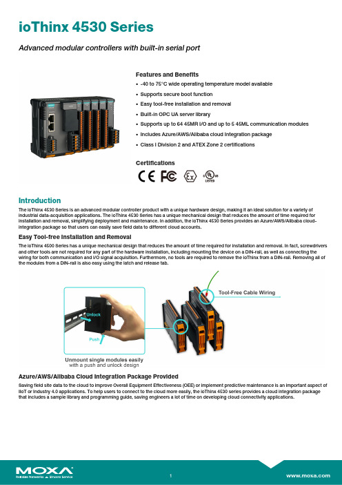
ioThinx4530SeriesAdvanced modular controllers with built-in serial portFeatures and Benefits•-40to75°C wide operating temperature model available•Supports secure boot function•Easy tool-free installation and removal•Built-in OPC UA server library•Supports up to6445MR I/O and up to545ML communication modules•Includes Azure/AWS/Alibaba cloud Integration package•Class I Division2and ATEX Zone2certificationsCertificationsIntroductionThe ioThinx4530Series is an advanced modular controller product with a unique hardware design,making it an ideal solution for a variety of industrial data-acquisition applications.The ioThinx4530Series has a unique mechanical design that reduces the amount of time required for installation and removal,simplifying deployment and maintenance.In addition,the ioThinx4530Series provides an Azure/AWS/Alibaba cloud-integration package so that users can easily save field data to different cloud accounts.Easy Tool-free Installation and RemovalThe ioThinx4500Series has a unique mechanical design that reduces the amount of time required for installation and removal.In fact,screwdrivers and other tools are not required for any part of the hardware installation,including mounting the device on a DIN-rail,as well as connecting the wiring for both communication and I/O signal acquisition.Furthermore,no tools are required to remove the ioThinx from a DIN-rail.Removing all of the modules from a DIN-rail is also easy using the latch and release tab.Azure/AWS/Alibaba Cloud Integration Package ProvidedSaving field site data to the cloud to improve Overall Equipment Effectiveness(OEE)or implement predictive maintenance is an important aspect of IIoT or Industry4.0applications.To help users to connect to the cloud more easily,the ioThinx4530series provides a cloud integration package that includes a sample library and programming guide,saving engineers a lot of time on developing cloud connectivity applications.SpecificationsComputerCPU Armv7Cortex-A7dual-core1GHzOS Linux kernel4.4(CIP,PREEMPT_RT),Debian9 Clock Real-time clock with capacitor backupDRAM512MB DDR3MRAM128kBStorage Pre-installed8GB eMMC(6GB reserved for the user) Storage Slot microSD Slots x1(up to32GB)Expansion Slots Up to64(with45MR I/O modules)Up to5(with45ML communication modules) Control LogicLanguage C/C++,PythonComputer InterfaceButtons Reset buttonInput/Output InterfaceRotary Switch0to9Ethernet Interface10/100BaseT(X)Ports(RJ45connector)Auto negotiation speedMagnetic Isolation Protection 1.5kV(built-in)Security FunctionsAuthentication Local databaseEncryption AES-256,SHA-256Security Protocols SSHv2Serial InterfaceConsole Port RS-232(TxD,RxD,GND),3-pin(115200,n,8,1)No.of Ports1x RS-232/422or2x RS-485-2wConnector Spring-type Euroblock terminalSerial Standards RS-232/422/485(software selectable)Baudrate300,600,1200,1800,2400,4800,9600,19200,38400,57600,115200bps Flow Control RTS/CTSParity None,Even,OddStop Bits1,2Data Bits7,8Serial SignalsRS-232TxD,RxD,RTS,CTS,GNDRS-422Tx+,Tx-,Rx+,Rx-,GNDRS-485-2w Data+,Data-,GNDSystem Power ParametersPower Connector Spring-type Euroblock terminalNo.of Power Inputs1Input Voltage12to48VDCPower Consumption1940mA@12VDCOver-Current Protection3A@25°COver-Voltage Protection55VDCOutput Current1A(max.)Field Power ParametersPower Connector Spring-type Euroblock terminalNo.of Power Inputs1Input Voltage12/24VDCOver-Current Protection5A@25°COver-Voltage Protection33VDCOutput Current2A(max.)Physical CharacteristicsWiring Serial cable,16to28AWGPower cable,12to26AWGStrip Length Serial cable,9to10mmPower cable,12to13mmHousing PlasticDimensions60.3x99x75mm(2.37x3.9x2.96in)Weight207.7g(0.457lb)Installation DIN-rail mountingStandards and CertificationsEMC EN55032/35EMI CISPR32,FCC Part15B Class AEMS IEC61000-4-2ESD:Contact:4kV;Air:8kVIEC61000-4-3RS:80MHz to1000MHz:3V/mIEC61000-4-4EFT:Power:2kV;Signal:1kVIEC61000-4-5Surge:Power:2kV;Signal:1kVIEC61000-4-6CS:10VIEC61000-4-8PFMFSafety UL61010-2-201Shock IEC60068-2-27Vibration IEC60068-2-6Hazardous Locations Class I Division2,ATEXMTBFTime856,064hrsStandards Telcordia SR332Environmental LimitsOperating Temperature ioThinx4533-LX:-20to60°C(-4to140°F)ioThinx4533-LX-T:-40to75°C(-40to167°F) Storage Temperature(package included)-40to85°C(-40to185°F)Ambient Relative Humidity5to95%(non-condensing)Altitude Up to4000mDeclarationGreen Product RoHS,CRoHS,WEEEWarrantyWarranty Period5yearsDetails See /warrantyPackage ContentsDevice1x ioThinx4530Series ControllerCable1x4-pin header to DB9console portInstallation Kit1x terminal block,5-pin,5.00mm1x terminal block,5-pin,3.81mm Documentation1x warranty card1x quick installation guide DimensionsTop/Side/Bottom PanelsSide CoverOrdering InformationModel NameLanguage Ethernet Interface Serial Interface No.of Support I/O Modules Operating Temp.ioThinx 4533-LXC/C++,Python 2x RJ45RS-232/RS-422/RS-48564-20to 60°C ioThinx 4533-LX-T C/C++,Python 2x RJ45RS-232/RS-422/RS-48564-40to 75°C Accessories (sold separately)I/O Modules45MR-1600Module for the ioThinx 4500Series,16DIs,24VDC,PNP,-20to 60°C operating temperature 45MR-1600-TModule for the ioThinx 4500Series,16DIs,24VDC,PNP,-40to 75°C operating temperature 45MR-1601Module for the ioThinx 4500Series,16DIs,24VDC,NPN,-20to 60°C operating temperature 45MR-1601-TModule for the ioThinx 4500Series,16DIs,24VDC,NPN,-40to 75°C operating temperature 45MR-2404Module for the ioThinx 4500Series,4relays,form A,-20to 60°C operating temperature 45MR-2404-TModule for the ioThinx 4500Series,4relays,form A,-40to 75°C operating temperature 45MR-2600Module for the ioThinx 4500Series,16DOs,24VDC,sink,-20to 60°C operating temperature 45MR-2600-TModule for the ioThinx 4500Series,16DOs,24VDC,sink,-40to 75°C operating temperature 45MR-2601Module for the ioThinx 4500Series,16DOs,24VDC,source,-20to 60°C operating temperature 45MR-2601-TModule for the ioThinx 4500Series,16DOs,24VDC,source,-40to 75°C operating temperature 45MR-2606Module for the ioThinx 4500Series,8DIs,24VDC,PNP,8DOs,24VDC,source,-20to 60°C operating temperature 45MR-2606-TModule for the ioThinx 4500Series,8DIs,24VDC,PNP,8DOs,24VDC,source,-40to 75°C operating temperature 45MR-3800Module for the ioThinx 4500Series,8AIs,0to 20mA or 4to 20mA,-20to 60°C operating temperature 45MR-3800-TModule for the ioThinx 4500Series,8AIs,0to 20mA or 4to 20mA,-40to 75°C operating temperature 45MR-3810Module for the ioThinx 4500Series,8AIs,-10to 10V or 0to 10V,-20to 60°C operating temperature 45MR-3810-T Module for the ioThinx 4500Series,8AIs,-10to 10V or 0to 10V,-40to 75°C operating temperature45MR-4420Module for the ioThinx4500Series,4AOs,0to10V or0to20mA or4to20mA,-20to60°C operatingtemperature45MR-4420-T Module for the ioThinx4500Series,4AOs,0to10V or0to20mA or4to20mA,-40to75°C operatingtemperature45MR-6600Module for the ioThinx4500Series,6RTDs,-20to60°C operating temperature45MR-6600-T Module for the ioThinx4500Series,6RTDs,-40to75°C operating temperature45MR-6810Module for the ioThinx4500Series,8TCs,-20to60°C operating temperature45MR-6810-T Module for the ioThinx4500Series,8TCs,-40to75°C operating temperaturePower Modules45MR-7210Module for the ioThinx4500Series,system and field power inputs,-20to60°C operating temperature 45MR-7210-T Module for the ioThinx4500Series,system and field power inputs,-40to75°C operating temperature 45MR-7820Module for the ioThinx4500Series,potential distributor module,-20to60°C operating temperature 45MR-7820-T Module for the ioThinx4500Series,potential distributor module,-40to75°C operating temperature Communication Modules45ML-5401Module for the ioThinx4530Series,4serial ports(RS-232/422/4853-in-1),-20to60°C operatingtemperature45ML-5401-T Module for the ioThinx4530Series,4serial ports(RS-232/422/4853-in-1),-40to75°C operatingtemperature©Moxa Inc.All rights reserved.Updated Oct17,2022.This document and any portion thereof may not be reproduced or used in any manner whatsoever without the express written permission of Moxa Inc.Product specifications subject to change without notice.Visit our website for the most up-to-date product information.。
艾特顿198950产品说明书

Eaton 198950Eaton Moeller® series Rapid Link - Speed controllers, 2.4 A, 0.75 kW, Sensor input 4, Actuator output 2, 230/277 V AC, PROFINET, HAN Q4/2, with manual override switchGeneral specificationsEaton Moeller® series Rapid Link Speed controller198950157 mm270 mm 220 mm 3.61 kgUL 61800-5-1 RoHS UL approval CEIEC/EN 61800-5-1RASP5-2422PNT-412R000S1Product NameCatalog NumberProduct Length/Depth Product Height Product Width Product Weight Certifications Catalog Notes Model Code3 fixed speeds and 1 potentiometer speedcan be switched over from U/f to (vector) speed control Connection of supply voltage via adapter cable on round or flexible busbar junction480 VIs the panel builder's responsibility. The specifications for the switchgear must be observed.400 V AC, 3-phase480 V AC, 3-phaseMeets the product standard's requirements.0.75 kW500 VMeets the product standard's requirements.-40 °C380 VSelector switch (Positions: REV - OFF - FWD)Thermo-click with safe isolationKey switch position AUTOKey switch position OFF/RESETControl unitInternal DC linkPTC thermistor monitoringTwo sensor inputs through M12 sockets (max. 150 mA) for quick stop and interlocked manual operationManual override switchKey switch position HANDPC connectionIGBT inverter2 Actuator outputs0 Hz200 %, IH, max. starting current (High Overload), For 2 seconds Generation change from RA-MO to RAMO 4.0Generation Change RASP4 to RASP5Generation change RAMO4 to RAMO5Generation change from RA-SP to RASP 4.0Configuration to Rockwell PLC for Rapid LinkGeneration Change RA-SP to RASP5Rapid Link 5 - brochureDA-SW-drivesConnect - InstallationshilfeDA-SW-Driver DX-CBL-PC-3M0DA-SW-USB Driver PC Cable DX-CBL-PC-1M5DA-SW-drivesConnect - installation helpDA-SW-USB Driver DX-COM-STICK3-KITDA-SW-drivesConnectMaterial handling applications - airports, warehouses and intra-logistics ETN.RASP5-2422PNT-412R000S1.edzIL034093ZUramo5_v31.dwgrasp5_v31.stpDA-DC-00004184.pdfDA-DC-00004514.pdfDA-DC-00003964.pdfDA-DC-00004508.pdfeaton-bus-adapter-rapidlink-speed-controller-dimensions-005.eps eaton-bus-adapter-rapidlink-speed-controller-dimensions-002.eps eaton-bus-adapter-rapidlink-speed-controller-dimensions-004.eps eaton-bus-adapter-rapidlink-speed-controller-dimensions-003.epsMains voltage - max10.11 Short-circuit ratingRated operational voltage10.4 Clearances and creepage distancesOutput at quadratic load at rated output voltage - max Output voltage - max10.2.3.1 Verification of thermal stability of enclosures Ambient storage temperature - minMains voltage - minFitted with:Output frequency - minStarting current - max Applikasjonsmerknader BrosjyrereCAD model Installeringsinstruksjoner mCAD model SertifiseringsrapporterTegningerevery 20 seconds, Power sectionRated conditional short-circuit current (Iq)10 kAAmbient operating temperature - max40 °CCommunication interfacePROFINET, optionalAssigned motor power at 115/120 V, 60 Hz, 1-phase1 HPOutput frequency - max500 HzSwitching frequency8 kHz, 4 - 32 kHz adjustable, fPWM, Power section, Main circuitFeaturesParameterization: drivesConnectParameterization: drivesConnect mobile (App) Parameterization: FieldbusParameterization: KeypadAmbient operating temperature - min-10 °CBraking current≤ 0.6 A (max. 6 A for 120 ms), Actuator for external motor brakeNumber of HW-interfaces (serial TTY)10.6 Incorporation of switching devices and componentsDoes not apply, since the entire switchgear needs to be evaluated.Nominal output current I2N2.4 A10.2.6 Mechanical impactDoes not apply, since the entire switchgear needs to be evaluated.10.3 Degree of protection of assembliesDoes not apply, since the entire switchgear needs to be evaluated.Product categorySpeed controllerRadio interference classC2, C3: depending on the motor cable length, the connected load, and ambient conditions. External radio interference suppression filters (optional) may be necessary.C1: for conducted emissions onlyHeat dissipation capacity Pdiss0 WRated control voltage (Uc)24 V DC (-15 %/+20 %, external via AS-Interface® plug) 230/277 V AC (external brake 50/60 Hz)Assigned motor power at 460/480 V, 60 Hz, 3-phase1 HPNumber of HW-interfaces (RS-422)Mains current distortion120 %ProtocolPROFINET IO10.9.2 Power-frequency electric strengthIs the panel builder's responsibility.Overvoltage categoryIIIDegree of protectionIP65NEMA 12Ambient storage temperature - max70 °CRated impulse withstand voltage (Uimp)2000 VConnectionPlug type: HAN Q4/2Overload currentAt 40 °CFor 60 s every 600 sFunctionsFor actuation of motors with mechanical brake3 fixed speeds1 potentiometer speedOutput at linear load at rated output voltage - max0.75 kWMains voltage tolerance380 - 480 V (-10 %/+10 %, at 50/60 Hz)Leakage current at ground IPE - max3.5 mAConverter typeU converter10.2.2 Corrosion resistanceMeets the product standard's requirements.Supply frequency50/60 Hz10.2.4 Resistance to ultra-violet (UV) radiationMeets the product standard's requirements.10.2.7 InscriptionsMeets the product standard's requirements.Shock resistance15 g, Mechanical, According to IEC/EN 60068-2-27, 11 ms, Half-sinusoidal shock 11 ms, 1000 shocks per shaftApplication in domestic and commercial area permittedYesNumber of inputs (analog)Number of phases (output)310.12 Electromagnetic compatibilityIs the panel builder's responsibility. The specifications for the switchgear must be observed.10.2.5 LiftingDoes not apply, since the entire switchgear needs to be evaluated.Number of HW-interfaces (RS-485)1Number of HW-interfaces (industrial ethernet)Efficiency97 % (η)System configuration typeAC voltageCenter-point earthed star network (TN-S network)Phase-earthed AC supply systems are not permitted.10.8 Connections for external conductorsIs the panel builder's responsibility.ProtectionFinger and back-of-hand proof, Protection against direct contact (BGV A3, VBG4)Braking voltage230/277 V AC -15 % / +10 %, Actuator for external motor brakeApplication in industrial area permittedYesClimatic proofingIn accordance with IEC/EN 50178< 95 %, no condensation10.9.3 Impulse withstand voltageIs the panel builder's responsibility.Overload current IL at 150% overload3.6 AInput current ILN at 150% overload2.5 ANumber of HW-interfaces (RS-232)Number of inputs (digital)4Current limitation0.2 - 2.4 A, motor, main circuitAdjustable, motor, main circuitCable lengthC2 ≤ 5 m, maximum motor cable lengthC1 ≤ 1 m, maximum motor cable lengthC3 ≤ 25 m, maximum motor cable length10.5 Protection against electric shockDoes not apply, since the entire switchgear needs to be evaluated.Mounting positionVerticalMains switch-on frequencyMaximum of one time every 60 seconds10.13 Mechanical functionThe device meets the requirements, provided the information in the instruction leaflet (IL) is observed.10.9.4 Testing of enclosures made of insulating materialIs the panel builder's responsibility.Heat dissipation per pole, current-dependent Pvid0 WElectromagnetic compatibility1st and 2nd environments (according to EN 61800-3)Resolution0.1 Hz (Frequency resolution, setpoint value)Assigned motor power at 460/480 V, 60 Hz1 HPRelative symmetric net voltage tolerance10 %Rated operational current (Ie)2.4 A at 150% overload (at an operating frequency of 8 kHz and an ambient air temperature of +40 °C)Number of outputs (analog)Rated operational power at 380/400 V, 50 Hz, 3-phase0.75 kWNumber of HW-interfaces (USB)Operating modeU/f controlBLDC motorsSynchronous reluctance motorsSensorless vector control (SLV)PM and LSPM motorsRated frequency - min45 HzDelay time< 10 ms, Off-delay< 10 ms, On-delayNumber of outputs (digital)2Power consumption32 W10.2.3.2 Verification of resistance of insulating materials to normal heatMeets the product standard's requirements.10.2.3.3 Resist. of insul. mat. to abnormal heat/fire by internal elect. effectsMeets the product standard's requirements.Number of HW-interfaces (other)Rated frequency - max66 HzVibrationResistance: 6 Hz, Amplitude 0.15 mmResistance: 10 - 150 Hz, Oscillation frequencyResistance: According to IEC/EN 60068-2-6Resistance: 57 Hz, Amplitude transition frequency on accelerationShort-circuit protection (external output circuits)Type 1 coordination via the power bus' feeder unit, Main circuit10.7 Internal electrical circuits and connectionsIs the panel builder's responsibility.Braking torqueAdjustable to 100 % (I/Ie), DC - Main circuit≤ 30 % (I/Ie)Relative symmetric net frequency tolerance10 %10.10 Temperature riseThe panel builder is responsible for the temperature rise calculation. Eaton will provide heat dissipation data for the devices.Number of HW-interfaces (parallel)Assigned motor power at 230/240 V, 60 Hz, 1-phase1 HPInterfacesNumber of slave addresses: 31 (AS-Interface®) Specification: S-7.4 (AS-Interface®)Max. total power consumption from AS-Interface® power supply unit (30 V): 250 mANumber of phases (input)3Eaton Corporation plc Eaton House30 Pembroke Road Dublin 4, Ireland © 2023 Eaton. Med enerett.Eaton is a registered trademark.All other trademarks are property of their respectiveowners./socialmedia27.5 W at 50% current and 90% speed 31.8 W at 100% current and 90% speed 33.5 W at 25% current and 50% speed 34.6 W at 50% current and 50% speed 35.1 W at 25% current and 0% speed 36.6 W at 100% current and 50% speed 36.8 W at 50% current and 0% speed 40.7 W at 100% current and 0% speed 2Max. 2000 mAbove 1000 m with 1 % performance reduction per 100 mHeat dissipation at current/speed Number of interfaces (PROFINET)Altitude。
- 1、下载文档前请自行甄别文档内容的完整性,平台不提供额外的编辑、内容补充、找答案等附加服务。
- 2、"仅部分预览"的文档,不可在线预览部分如存在完整性等问题,可反馈申请退款(可完整预览的文档不适用该条件!)。
- 3、如文档侵犯您的权益,请联系客服反馈,我们会尽快为您处理(人工客服工作时间:9:00-18:30)。
TOSHIBA InGaAℓP LEDTLRE53T(F),TLRME53T(F),TLSE53T(F),TLOE53T(F),TLYE53T(F), TLPYE53T(F),TLGE53T(F),TLFGE53T(F),TLPGE53T(F)Panel Circuit Indicators•Lead(Pb)-free products (lead: Sn-Ag-Cu)•3mm package•InGaAℓP technology•All plastic mold•Transparent lens•Lineup: 6 colors (red, orange, yellow, pure yellow, green and pure green)•High intensity light emission•Excellent low current light output•Applications: message boards, security devices and dashboarddisplaysLineupUnit: mmJEDEC ―JEITA ―TOSHIBA 4-4E1A Weight: 0.14 g(Typ.)Product Name Color Material TLRE53T(F) RedTLRME53T(F) RedTLSE53T(F) RedTLOE53T(F) OrangeTLYE53T(F) Yellow TLPYE53T(F) PureYellow TLGE53T(F) Green TLFGE53T(F) Green TLPGE53T(F) PureGreenP InGaA lAbsolute Maximum Ratings (Ta = 25°C)Product Name Forward CurrentI F (mA)Reverse VoltageV R (V)Power DissipationP D (mW)OperatingTemperatureT opr (°C)StorageTemperatureT stg (°C)TLRE53T(F) 50 4 120TLRME53T(F) 50 4 120TLSE53T(F) 50 4 120TLOE53T(F) 50 4 120TLYE53T(F) 50 4 120TLPYE53T(F) 50 4 120TLGE53T(F) 50 4 120TLFGE53T(F) 50 4 120TLPGE53T(F) 50 4 120−40~100 −40~120Note: Using continuously under heavy loads (e.g. the application of high temperature/current/voltage and the significant change in temperature, etc.) may cause this product to decrease in the reliability significantly even if the operating conditions (i.e. operating temperature/current/voltage, etc.) are within the absolute maximum ratings.Please design the appropriate reliability upon reviewing the Toshiba Semiconductor Reliability Handbook(“Handling Precautions”/“Derating Concept and Methods”) and individual reliability data (i.e. reliability testreport and estimated failure rate, etc).Electrical and Optical Characteristics (Ta = 25°C)Typ. Emission Wavelength Luminous IntensityI VForward VoltageV FReverse CurrentI RProduct NameλdλPΔλI F Min Typ.I F Typ.Max I F Max V R TLRE53T(F) 630 (644) 20 20 153 400 20 1.9 2.4 20 50 4TLRME53T(F) 626 (636) 23 20 272 600 20 1.9 2.4 20 50 4TLSE53T(F) 613 (623) 20 20 272 800 20 1.9 2.4 20 50 4TLOE53T(F) 605 (612) 20 20 272 100020 2.0 2.4 20 50 4TLYE53T(F) 587 (590) 17 20 272 800 20 2.0 2.4 20 50 4TLPYE53T(F) 580 (583) 14 20 153 450 20 2.0 2.4 20 50 4TLGE53T(F) 571 (574) 17 20 153 400 20 2.0 2.4 20 50 4TLFGE53T(F) 565 (568) 15 20 85 200 20 2.0 2.4 20 50 4TLPGE53T (F) 558 (562) 14 20 47.6130 20 2.1 2.4 20 50 4 Unit nmmAmcdmAVmAμA V PrecautionsPlease be careful of the following:•Soldering temperature: 260°C max, soldering time: 3 s max(soldering portion of lead: up to 1.6 mm from the body of the device)•If the lead is formed, the lead should be formed up to 1.6 mm from the body of the device without forming stress to the resin. Soldering should be performed after lead forming.•This visible LED lamp also emits some IR light.If a photodetector is located near the LED lamp, please ensure that it will not be affected by this IR light.R e l at i v e l u m i n o u si n t e n s i t yForward voltage V F (V) I F – V FF o r w a r d cu r r e n t I F (m A )Forward current I F (mA)I V – I FL u m i no u s i n t e n si t y I V (m c d )Case temperature Tc (°C) I V – TcR e l a t i v e l u mi n o u s in t e n s i t y I VWavelength λ (nm)Relative luminous intensity – WavelengthAmbient temperature Ta (°C)I F – TaA l l o w a b l e fo r w a r d c u r r e n t I F (m A )Radiation patternTa = 25°C30°0°60° 90° 90°30° 60° 1.00.80.6 0.4 0.2 0 80° 70° 50° 40°20°10°70° 80° 50° 40° 20° 10°20 −20 800.1310.30.5 0 4060 060040802012020406080 100R e l at i v e l u m i n o u si n t e n s i t yForward voltage V F (V) I F – V FF o r w a r d c ur r e n t I F (m A )Forward current I F (mA)I V – I FL u m i n ou s i n t e ns i t y I V (m c d )Case temperature Tc (°C) I V – TcR e l a t i v e l u mi n o u s in t e n s i t y I VWavelength λ (nm)Relative luminous intensity – WavelengthAmbient temperature Ta (°C)I F – TaA l l o w a b l e fo r w a r d c u r r e n t I F (m A )Radiation patternTa = 25°C30°0°60° 90° 90°30° 60° 1.00.80.6 0.4 0.2 0 80° 70° 50° 40°20°10°70° 80° 50° 40° 20° 10°60040802012020406080100 20 −20 800.1310.30.5 0 4060 510R e l at i v e l u m i n o u si n t e n s i t yForward voltage V F (V) I F – V FF o r w a r d cu r r e n t I F (m A )Forward current I F (mA)I V – I FL u m i no u s i n t e n si t y I V (m c d )Case temperature Tc (°C) I V – TcR e l a t i v e l u mi n o u s in t e n s i t y I VWavelength λ (nm)Relative luminous intensity – WavelengthAmbient temperature Ta (°C)I F – TaA l l o w a b l e fo r w a r d c u r r e n t I F (m A )Radiation patternTa = 25°C30°0°60° 90° 90°30° 60° 1.00.80.6 0.4 0.2 0 80° 70° 50° 40°20°10°70° 80° 50° 40° 20°10°60040802012020406080 100 20 −20 800.1310.30.5 0 4060R e l at i v e l u m i n o u si n t e n s i t yForward voltage V F (V) I F – V FF o r w a r d c ur r e n t I F (m A )Forward current I F (mA)I V – I FL u m i no u s i n t e n si t y I V (m c d )Case temperature Tc (°C) I V – TcR e l a t i v e l u mi n o u s in t e n s i t y I VWavelength λ (nm)Relative luminous intensity – WavelengthAmbient temperature Ta (°C)I F – TaA l l o w a b l e fo r w a r d c u r r e n t I F (m A )Radiation patternTa = 25°C30°0°60° 90° 90°30° 60° 1.00.80.6 0.4 0.2 0 80° 70° 50° 40°20°10°70° 80° 50° 40° 20° 10°60040802012020406080 10020 −20 800.1310.30.5 0 4060R e l at i v e l u m i n o u si n t e n s i t yForward voltage V F (V) I F – V FF o r w a r d c ur r e n t I F (m A )Forward current I F (mA)I V – I FL u m i no u s i n t e n si t y I V (m c d )Case temperature Tc (°C) I V – TcR e l a t i v e l u mi n o u s in t e n s i t y I VWavelength λ (nm)Relative luminous intensity – WavelengthAmbient temperature Ta (°C)I F – TaA l l o w a b l e fo r w a r d c u r r e n t I F (m A )Radiation patternTa = 25°C30°0°60° 90° 90°30° 60° 1.00.80.6 0.4 0.2 0 80° 70° 50° 40°20°10°70° 80° 50° 40° 20° 10°60040802012020406080 10020 −20 800.1310.30.5 0 4060100R e l a t i v e l u m i n o u s i n t e n s i t yForward voltage V F (V)I F – V FF o r w a r d c u r r e n t I F (m A )Forward current I F (mA)I V– I FL u m in o u s i n t e n s i t y I V (m c d )Case temperature Tc (°C)I V – TcR e l a t iv e l u m i n o u s i n t e n s i t y I VWavelength λ (nm)Relative luminous intensity – WavelengthAmbient temperature Ta (°C)I F – TaA l l o w a b l e f o r w a r d c u r r e n t I F (m A )Radiation patternTa = 25°C30°0°60° 90° 90°30° 60° 1.00.80.6 0.4 0.2 0 80° 70° 50° 40°20°10°70° 80° 50° 40° 20° 10°60040802012020406080 100 20 −20 805 0.131010.30.50 40 60 100R e l at i v e l u m i n o u si n t e n s i t yForward voltage V F (V) I F – V FF o r w a r d c ur r e n t I F (m A )Forward current I F (mA)I V – I FL u m i no u s i n t e n si t y I V (m c d )Case temperature Tc (°C) I V – TcR e l a t i v e l u mi n o u s in t e n s i t y I VWavelength λ (nm)Relative luminous intensity – WavelengthAmbient temperature Ta (°C)I F – TaA l l o w a b l e fo r w a r d c u r r e n t I F (m A )Radiation patternTa = 25°C30°0°60° 90° 90°30° 60° 1.00.80.6 0.4 0.2 0 80° 70° 50° 40°20°10°70° 80° 50° 40° 20° 10°60040802012020406080100 20 −20 800.1310.30.5 0 4060 5 10100R e l a t i v e l u m i n o u s i n t e n s i t yForward voltage V F (V) IF – V FFo r w a r d c u r r e n t I F (m A )Forward current I F (mA)I V – I FL u m i no u s i n t e n s i t y I V (m c d )Case temperature Tc (°C) I V – TcR e l a t i ve l u m i n o u s i n t e n s i t y I VWavelength λ (nm)Relative luminous intensity – WavelengthAmbient temperature Ta (°C)I F – TaA l l o w a b l e f o r w a r d c u r r e n t I F (m A )Radiation patternTa = 25°C30°0°60° 90° 90°30° 60° 1.00.80.6 0.4 0.2 0 80° 70° 50° 40°20°10°70° 80° 50° 40° 20° 10°60040802012020406080 100 560520640540580 600 620 20 −20805 0.131010.30.5 0 40 60 100TLPGE53T(F)R e l a t i v e l u m i n o u si n t e n s i t yForward voltage V F (V) I F – V FF o r w a r d cu r r e n t I F (m A )Forward current I F (mA)I V – I FL u m i n ou s i n t e ns i t y I V (m c d )Case temperature Tc (°C) I V – TcR e l a t i v e l u mi n o u s i n te n s i t y I VWavelength λ (nm)Relative luminous intensity – WavelengthAmbient temperature Ta (°C)I F – TaA l l o w a b l e f or w a r d c u r r e n t I F (m A )Radiation patternTa =25°C30°0°60° 90° 90°30° 60° 1.00.80.6 0.4 0.2 0 80° 70° 50° 40°20°10°70° 80° 50° 40° 20°10°60040802012020406080100 20 −20 800.1310.30.5 0 4060 5 10RESTRICTIONS ON PRODUCT USE20070701-EN •The information contained herein is subject to change without notice.•TOSHIBA is continually working to improve the quality and reliability of its products. Nevertheless, semiconductor devices in general can malfunction or fail due to their inherent electrical sensitivity and vulnerability to physical stress. It is the responsibility of the buyer, when utilizing TOSHIBA products, to comply with the standards of safety in making a safe design for the entire system, and to avoid situations in which a malfunction or failure of such TOSHIBA products could cause loss of human life, bodily injury or damage to property.In developing your designs, please ensure that TOSHIBA products are used within specified operating ranges as set forth in the most recent TOSHIBA products specifications. Also, please keep in mind the precautions and conditions set forth in the “Handling Guide for Semiconductor Devices,” or “TOSHIBA Semiconductor Reliability Handbook” etc.• The TOSHIBA products listed in this document are intended for usage in general electronics applications (computer, personal equipment, office equipment, measuring equipment, industrial robotics, domestic appliances, etc.).These TOSHIBA products are neither intended nor warranted for usage in equipment that requires extraordinarily high quality and/or reliability or a malfunction or failure of which may cause loss of human life or bodily injury (“Unintended Usage”). Unintended Usage include atomic energy control instruments, airplane or spaceship instruments, transportation instruments, traffic signal instruments, combustion control instruments, medical instruments, all types of safety devices, etc.. Unintended Usage of TOSHIBA products listed in his document shall be made at the customer’s own risk.•The products described in this document shall not be used or embedded to any downstream products of which manufacture, use and/or sale are prohibited under any applicable laws and regulations.• The information contained herein is presented only as a guide for the applications of our products. No responsibility is assumed by TOSHIBA for any infringements of patents or other rights of the third parties which may result from its use. No license is granted by implication or otherwise under any patents or other rights of TOSHIBA or the third parties.•GaAs(Gallium Arsenide) is used in this product. The dust or vapor is harmful to the human body. Do not break, cut, crush or dissolve chemically.• Please contact your sales representative for product-by-product details in this document regarding RoHS compatibility. Please use these products in this document in compliance with all applicable laws and regulations that regulate the inclusion or use of controlled substances. Toshiba assumes no liability for damage or losses occurring as a result of noncompliance with applicable laws and regulations.。