CD74HCT258EE4中文资料
74HCT0474HC04中文资料
TA =25℃
TA eb40 to 85℃
TA eb55 to 125℃
单位
典型
保证界限
tPHL,tPLH
最大传输延迟时间
2.0V
55
95
120
145
ns
4.5V
11
19
24
29
6.0V
9
16
20
24
tTLH,tTHL
Maximum Output Rise and Fall Time最大输出上升和下降时间
0.26
0.33
0.4
V
6.0V
0.2
0.26
0.33
0.4
IIN
最大输入电流
VIN=VCC or GND
6.0V
±0.1
±1.0
±1.0
μA
ICC
电源电流
VIN=VCC or GND IOUT=0 μA
6.0V
2.0
20
40
μA
交流电气特性:
Symbol 符号
Parameter 参数
条件
典型
Guaranteed Limit 保证极限
-1.5 to Vcc+1.5V
直流输出电压
-0.5 to Vcc+0.5V
钳位二极管电流
±20mA
直流输出电流,每个引脚(输出)
±25mA
功耗
600mW
建议操作条件:
Operating Conditions操作条件
最小
最大
单位
Supply Voltage电源电压(VCC)
2
6
V
DC输入或输出电压(输入电压,输出电压)
74HC系列名词解释
型号器件名称厂牌[数据表]74HC00四2输入端与非门TI[DA TA]74HC01四2输入端与非门(OC)74HC02四2输入端或非门TI[DA TA]74HC03四2输入端与非门(OC)TI[DATA]74HC04六反相器TI[DA TA]74HC05HEX INVERTERS74HC08四2输入端与门TI[DATA]74HC09QUADRUPLE 2-INPUT POSITIVE-AND 74HC10三3输入端与非门TI[DA TA]74HC11三3输入端与门TI[DATA]74HC14双4输入端与非门TI[DA TA]74HC20双4输入端与非门TI[DA TA]74HC21双4输入端与门TI[DATA]74HC27三3输入端或非门TI[DA TA]74HC308输入端与非门TI[DA TA]74HC32四2输入端或门TI[DATA]74HC424线-10线译码器(BCD输入)TI[DATA]74HC73DUAL J-K FLIP-FLOPTI[DATA]74HC74双上升沿D型触发器TI[DATA]74HC754-BIT BISTABLE LATCHTI[DA TA]74HC85A四位数值比较器TI[DATA]74HC86四2输入端异或门TI[DA TA]74HC93双4输入端与非门TI[DA TA]74HC107双主-从J-K触发器TI[DA TA]74HC109双J-K触发器TI[DA TA]74HC112双下降沿J-K触发器TI[DATA]74HC123可重触发双稳态触发器TI[DA TA]74HC125四总线缓冲器TI[DA TA]74HC126四总线缓冲器74HC132四2输入端与非门74HC13313-INPUT POSITIVE-NAND74HC137地址锁存3线-8线译码器74HC1383线-8线译码器74HC139双2线-4线译码器74HC14710线-4线优先编码器74HC1488-LINE TO 3-LINE PRIORITY ENCODERS 74HC1518-INPUT MULTIPLEXER74HC153DUAL 4-INPUT MULTIPLEXER74HC1544线-16线译码器74HC157四2选1数据选择器74HC158四2选1数据选择器74HC160DECADE COUNTER74HC1614位二进制同步计数器74HC162DECADE COUNTER74HC1634-BIT BINARY PRESETTABLE COUNTER 74HC1648位移位寄存器74HC1658位并行输入/串行输出寄存器74HC1668位并行输入/串行输出移位寄存器TI,PHI 74HC1734位D型寄存器TI74HC174HEX D-TYPE FLIP-FLOP WITH RESETTI 74HC175四上升沿D型触发器TI74HC190十进制同步加/减计数器TI74HC1914位二进制同步加/减计数器TI74HC192BCD二进制同步加/减计数器TI74HC193可预置4位二进制加/减计数器TI74HC1944位并入/串入-并出/串出移位寄存TI74HC1954位移位寄存器TI74HC221双单稳态触器TI74HC2373-8线译码器(带地址锁存)TI74HC2383-8线译码器TI74HC239双2-4线译码器74HC240八反相缓冲/线驱动/线接收器TI74HC241八缓冲/线驱动/线接收器TI74HC243四总线收发器TI74HC244八缓冲/线驱动/线接收器TI,FSC74HC245八双向总线发送/接发器TI,FSC74HC2518选1数据选择器74HC253双4选1数据选择器74HC257四2选1数据选择器74HC258四2选1数据选择器74HC2598位可寻址锁存器74HC266QUADRUPLE 2-INPUT EXCLUSIVE-NOR 74HC273八D触发器74HC2809位奇偶产生器/校验器TI74HC2834位二进制超位全加器74HC297DIGITAL PHASE-LOCKED-LOOP74HC2998位双向通用移位/存储寄存器74HC354带锁存三态8-1多路转换开关74HC365六总线驱动器74HC366六反相总线驱动器74HC367六总线驱动器74HC368六反相总线驱动器74HC373六D型锁存器74HC374六上升沿D型触发器74HC3754-BIT BISTABLE LATCH74HC377六上升沿D型触发器74HC3786-BIT D-TYPE FLIP-FLOP74HC379QUADRUPLE D-TYPE FLIP-FLOP74HC390双十进制计数器74HC393双4位二进制计数器74HC4002高速CMOS双4输入端或非门74HC4015高速CMOS双4位串入/并出移位寄存器74HC4016高速CMOS四传输门74HC4017高速CMOS十进制计数/分配器74HC4020高速CMOS14级串行二进制计数/分频器74HC4024高速CMOS7级二进制串行计数/分频器74HC4040高速CMOS12级二进制串行计数/分频器74HC4046A高速CMOS锁相环74HC4049高速CMOS六反相缓冲/变换器74HC4050高速CMOS六同相缓冲/变换器74HC4051高速CMOS八选一模拟开关74HC4052高速CMOS双4选1模拟开关74HC4053高速CMOS三组二路模拟开关74HC4059高速CMOS“N”分频计数器74HC4060高速CMOS14级二进制串行计数/分频器74HC406114-STAGE BINARY COUNTER/OSCILLATOR 74HC4066高速CMOS四传输门74HC4067高速CMOS16选1模拟开关74HC4075高速CMOS三3输入端或门74HC4078A8-INPUT OR/NOR74HC4094高速CMOS8位移位存储总线寄存器74HC40103高速CMOS8位可预置同步二进制减法计数器74HC40105高速CMOS先入先出FI-FD寄存器74HC423 双单稳态振荡器TI[DA TA]74HC4316高速CMOS四模拟开关TI74HC4351ANALOG MULTIPLEXER/DEMULTIPLEXERTI 74HC4352ANALOG MULTIPLEXER/DEMULTIPLEXERTI 74HC4511高速CMOSBCD锁存,7段译码,驱动器74HC4514高速CMOS4位锁存,4线-16线译码器74HC4515高速CMOS4位锁存,4线-16线译码器74HC4518高速CMOS双BCD同步加计数器74HC4520高速CMOS双4位二进制同步加计数器74HC4538高速CMOS精密双单稳TI,INT(HAR)74HC533三态八D锁存器74HC534三态八D锁存器74HC540八路三态收发缓冲器(反相)74HC541八路三态收发缓冲器(同相)74HC563三态八D锁存器74HC564三态八D锁存器74HC573四3选1数据选择器74HC574双4选1数据选择器74HC590A8位二进制计数器TI74HC5948位移位寄存器TI74HC5958位移位三态寄存器TI,ST[DATA],FSC,PHI 74HC5978位移位寄存器74HC651OCTAL BUS TRANSCEIVER/REGISTERTI 74HC652OCTAL BUS TRANSCEIVER/REGISTERTI 74HC664OCTAL BUS TRANSCEIVERTI74HC665OCTAL BUS TRANSCEIVERTI74HC6704-BY-4 REGISTER FILE74HC6828-BIT MAGNITUDE COMPARA TORS74HC6848-BIT MAGNITUDE COMPARA TORSTI74HC6888-BIT MAGNITUDE COMPARA TOR74HC7001QUADRUPLE POSITIVE-ANDTI74HC7002QUADRUPLE POSITIVE-NORTI74HC7032QUADRUPLE POSITIVE-ORTI74HC70746-SECTION MULTIFUNCTION CIRCUITTI 74HC7046A压控锁相环74HC7266QUAD 2-INPUT EXCLUSIVE-NOR GATE 74HCU04HEX INVERTERTI74HC4543高速CMOSBCD七段锁存译码,驱动器74HC47248-BIT ADDRESSABLE LATCHES74HC623OCTAL BUS TRANSCEIVERTI74HC640OCTAL BUS TRANSCEIVER74HC643OCTAL BUS TRANSCEIVERTI74HC645OCTAL BUS TRANSCEIVERTI74HC646OCTAL BUS TRANSCEIVER/REGISTER74HC648OCTAL BUS TRANSCEIVER/REGISTERTI。
CD74HC154M96E4,CD74HC154M96G4,CD74HC154M96,CD74HC154M96,CD74HC154M96, 规格书,Datasheet 资料
67
M (SOIC) Package (Note 2). . . . . . . . . . . . . . . . . . .
46Leabharlann Maximum Junction Temperature . . . . . . . . . . . . . . . . . . . . . . . 150oC
Maximum Storage Temperature Range . . . . . . . . . .-65oC to 150oC
1
芯天下--/
CD54HC154, CD74HC154, CD54HCT154, CD74HCT154
Functional Diagram
A0 23 A1 22 A2 21
20 A3
E1 18 E2 19
1 Y0
2 Y1
3 Y2
4 Y3
5 Y4
6 Y5
7 Y6
8 Y7
[ /Title (CD74 HC154 , CD74 HCT15 4) /Subject (High Speed CMOS Logic 4-to-16 Line Decod er/Dem
Features
• Two Enable Inputs to Facilitate Demultiplexing and Cascading Functions
Data sheet acquired from Harris Semiconductor SCHS152D
September 1997 - Revised June 2004
CD54HC154, CD74HC154, CD54HCT154, CD74HCT154
High-Speed CMOS Logic 4- to 16-Line Decoder/Demultiplexer
74HC258DB,118,74HC258DB,112,74HC258D,652,74HC258D,653,74HC258N,652, 规格书,Datasheet 资料

1.General descriptionThe 74HC258is a high-speed Si-gate CMOS device and is pin compatible with low power Schottky TTL (LSTTL). The 74HC258 is specified in compliance with JEDEC standard no.7A.The 74HC258 has four identical 2-input multiplexers with 3-state outputs, which select 4bits of data from two sources and is controlled by a common data select input (S).The data inputs from source 0(1I0to 4I0)are selected when input S is LOW and the data inputs from source 1 (1I1to 4I1) are selected when S is HIGH.Data appears at the outputs (1Y to 4Y) in inverted form from the select inputs.The 74HC258is the logic implementation of a 4-pole,2-position switch,where the position of the switch is determined by the logic levels applied to S. The outputs are forced to a high-impedance OFF-state when OE is HIGH.The logic equations for the outputs are:The 74HC258 is identical to the 74HC257 but has inverting outputs.2.FeaturesI 3-state outputs interface directly with system bus I Low-power dissipation I Inverting data pathI Complies with JEDEC standard no.7A IESD protection:N HBM JESD22-A114E exceeds 2000V N MM JESD22-A115-A exceeds 200V I Multiple package optionsI Specified from −40°C to +85°C and from −40°C to +125°C.74HC258Quad 2-input multiplexer; 3-state; invertingRev. 04 — 14 April 2008Product data sheet1Y OE 1I1S ×1I0S ×+()×=2Y OE 2I1S ×2I0S ×+()×=3Y OE 3I1S ×3I0S ×+()×=4Y OE 4I1S ×4I0S ×+()×=3.Ordering information4.Functional diagramTable 1.Ordering informationType number PackageTemperature rangeName DescriptionVersion 74HC258N −40°C to +125°C DIP16plastic dual in-line package; 16leads (300mil)SOT38-474HC258D −40°C to +125°C SO16plastic small outline package; 16leads; body width 3.9mmSOT109-174HC258DB−40°C to +125°CSSOP16plastic shrink small outline package; 16leads; bodywidth 5.3mmSOT338-1Fig 1.Functional diagram Fig 2.Logic symbol001aab9682S1I01Y 42Y 73Y 94Y 12OE11531I152I062I1113I0103I1144I0134I1SELECTOR3-ST ATE MULTIPLEXER OUTPUTS001aab9661I01I12I02I13I03I14I04I1S 1Y 2Y 3Y 4Y11297413OE151410116532Fig 3.IEC logic symbol Fig 4.Logic diagram001aab967129715EN1G11MUX41314101165321001aab9691I01I12I02I13I03I14I04I1SOE 1Y2Y3Y4Y5.Pinning information5.1Pinning5.2Pin descriptionFig 5.Pin configuration258S V CC 1I0OE 1I14I01Y 4I12I04Y 2I13I02Y 3I1GND3Y001aab90412345678109121114131615Table 2.Pin descriptionSymbol Pin DescriptionS 1common data select input 1I02data input 1 from source 01I13data input 1 from source 11Y 43-state multiplexer output 1; inverted 2I05data input 2 from source 02I16data input 2 from source 12Y 73-state multiplexer output 2; inverted GND 8ground (0V)3Y 93-state multiplexer output 3; inverted 3I110data input 3 from source 13I011data input 3 from source 04Y 123-state multiplexer output 4; inverted 4I113data input 4 from source 14I014data input 4 from source 0OE 15output enable input (active LOW)V CC16positive supply voltage6.Functional descriptionTable 3.Function table[1]Control Input OutputOE S nl0nI1nYH X X X ZL L L X HL L H X LL H X L HL H X H L[1]H=HIGH voltage level;L=LOW voltage level;X=don’t care;Z=high-impedance OFF-state.7.Limiting valuesTable 4.Limiting valuesIn accordance with the Absolute Maximum Rating System (IEC 60134). Voltages are referenced to GND (ground = 0 V). Symbol Parameter Conditions Min Max Unit V CC supply voltage−0.5+7.0VI IK input clamping current V I <−0.5V or V I>V CC+0.5 V[1]-±20mA I OK output clamping current V O<−0.5V or V O>V CC+0.5V[1]-±20mA I O output current V O =−0.5V to V CC+0.5V-±35mA I CC supply current-70mA I GND ground current−70-mA T stg storage temperature−65+150°C P tot total power dissipation T amb =−40°C to +125°CDIP16 package[2]-750mWSO16 package[3]-500mWSSOP16 package[4]-500mW[1]The input and output voltage ratings may be exceeded if the input and output current ratings are observed.[2]P tot derates linearly with 12mW/K above 70°C.[3]P tot derates linearly with 8mW/K above 70°C.[4]P tot derates linearly with 5.5mW/K above 60°C.8.Recommended operating conditions9.Static characteristicsTable 5.Recommended operating conditionsSymbol Parameter ConditionsMin Typ Max Unit V CC supply voltage 2.0 5.0 6.0V V I input voltage 0-V CC V V O output voltage 0-V CC V T amb ambient temperature−40-+125°C ∆t/∆Vinput transition rise and fall rateV CC = 2.0 V --625ns V CC = 4.5 V - 1.67139ns V CC = 6.0 V --83nsTable 6.Static characteristicsAt recommended operating conditions; voltages are referenced to GND (ground =0V).Symbol Parameter Conditions25°C −40°C to +85°C −40°C to +125°C Unit MinTyp Max Min Max Min Max V IHHIGH-level input voltageV CC =2.0V 1.5 1.2- 1.5- 1.5-V V CC =4.5V 3.15 2.4- 3.15- 3.15-V V CC =6.0V4.2 3.2- 4.2- 4.2-V V ILLOW-level input voltageV CC =2.0V -0.80.5-0.5-0.5V V CC =4.5V - 2.1 1.35- 1.35- 1.35V V CC =6.0V- 2.81.8- 1.8- 1.8VV OHHIGH-level output voltageV I =V IH or V ILI O =−20µA; V CC =2.0V 1.9 2.0- 1.9- 1.9-V I O =−20µA; V CC =4.5V 4.4 4.5- 4.4- 4.4-V I O =−20µA; V CC =6.0V 5.96.0- 5.9- 5.9-V I O =−6mA; V CC =4.5V 3.98 4.32- 3.84- 3.7-V I O =−7.8mA; V CC =6.0V5.48 5.81- 5.34- 5.2-VV OLLOW-level output voltageV I =V IH or V ILI O =20µA; V CC =2.0V -00.1-0.1-0.1V I O =20µA; V CC =4.5V -00.1-0.1-0.1V I O =20µA; V CC =6.0V -00.1-0.1-0.1V I O =6mA; V CC =4.5V -0.150.26-0.33-0.4V I O =7.8mA; V CC =6.0V-0.160.26-0.33-0.4V I I input leakage current V I =V CC or GND;V CC =6.0V--±0.1-±1.0-±1.0µA I OZ OFF-state output currentV I =V IH or V IL ; V CC =6.0V;V O =V CC or GND; I O =0A--±0.5-±5.0-±10µA I CC supply current V I =V CC or GND; I O =0A;V CC =6.0V --8-80-160µA C Iinputcapacitance- 3.5-----pF10.Dynamic characteristics[1]t pd is the same as t PHL and t PLH .[2]t en is the same as t PZH and t PZL .[3]t dis is the same as t PHZ and t PLZ .[4]t t is the same as t THL and t TLH .[5]C PD is used to determine the dynamic power dissipation (P D in µW).P D =C PD ×V CC 2×f i ×N +∑(C L ×V CC 2×f o )where:f i =input frequency in MHz;f o =output frequency in MHz;C L =output load capacitance in pF;V CC =supply voltage in V;N =number of inputs switching;∑(C L ×V CC 2×f o )= sum of outputs.Table 7.Dynamic characteristics GND =0V; for test circuit see Figure 8.SymbolParameterConditions25°C −40°C to +125°C Unit MinTypMaxMax (85°C)Max (125°C)t pdpropagation delay nl0, nI1to nY; see Figure 6[1]V CC = 2.0 V -3095120145ns V CC = 4.5 V -11192429ns V CC = 6.0 V-9162025ns V CC = 5.0 V; C L =15 pF -9---ns S to nY; see Figure 6V CC = 2.0 V -47140175210ns V CC = 4.5 V -17283542ns V CC = 6.0 V-14243036ns V CC = 5.0 V; C L =15 pF-14---ns t enenable timeOE to nY; see Figure 7[2]V CC = 2.0 V -39140175210ns V CC = 4.5 V -14283542ns V CC = 6.0 V-11243036ns t disdisable timeOE to nY; see Figure 7[3]V CC = 2.0 V -55150190225ns V CC = 4.5 V -20303845ns V CC = 6.0 V-16263338ns t ttransition timesee Figure 6[4]V CC = 2.0 V -14607590ns V CC = 4.5 V -5121518ns V CC = 6.0 V-4101315ns C PDpower dissipation capacitanceper multiplexer;V I =GND to V CC[5]-55---pF11.WaveformsMeasurement points are given in Table 8.V OL and V OH are typical output voltage levels that occur with the output load.Fig 6.Input (nI0,nI1and S) to output (nY) propagation delays and output transition times001aab970S, nI0, nI1inputnY outputV MV OHV IGNDV OLt PHLt THLt TLHt PLHV MMeasurement points are given in Table 8.V OL and V OH are typical output voltage levels that occur with the output load.Fig 7.Enable and disable times V MOE inputoutput LOW to OFF OFF to LOWoutputHIGH to OFF OFF to HIGHV M001aab971t ft rt PLZV Mt PZLt PHZt PZHV XV Youtputs enabledoutputs disabledoutputs enabledV OHV IGNDGNDV OL V CCTable 8.Measurement pointsInput Output V M V M V XV Y0.5× V CC0.5× V CC0.1× V CC0.9× V CCTest data is given in T able 9.Definitions test circuit:R T = Termination resistance should be equal to output impedance Z o of the pulse generator.C L = Load capacitance including jig and probe capacitance.R L = Load resistance.S1 = Test selection switch.Fig 8.Test circuit for measuring switching times V M V Mt Wt W10 %90 %0 VV IV I negative pulsepositive pulse0 VV MV M 90 %10 %t ft r t rt f 001aad983DUTV CCV CCV IV OR TR LS1C LopenGTable 9.Test dataSupply voltageInput Load S1V CC V I t r = t f C L R L t PZL , t PLZ t PZH , t PHZ t PHL , t PLH 2.0 V V CC 6 ns 50 pF 1 k ΩV CC GND open 4.5 V V CC 6 ns 50 pF 1 k ΩV CC GND open 6.0 V V CC 6 ns 50 pF 1 k ΩV CC GND open 5.0 VV CC6 ns15 pF1 k ΩV CCGNDopen12.Package outlineFig 9.Package outline SOT38-4 (DIP16)REFERENCESOUTLINE VERSION EUROPEAN PROJECTIONISSUE DATE IECJEDECJEITASOT38-495-01-1403-02-13M Hc(e )1M EALs e a t i n g p l a n eA 1w Mb 1b 2eDA 2Z16198Epin 1 indexb0510 mmscaleNote1. Plastic or metal protrusions of 0.25 mm (0.01 inch) maximum per side are not included.UNIT Amax.12b 1(1)(1)(1)b 2c D E e M Z H L mm DIMENSIONS (inch dimensions are derived from the original mm dimensions)A min. A max.b max.w M E e 11.731.300.530.380.360.2319.5018.55 6.486.20 3.603.050.2542.547.628.257.8010.08.30.764.20.51 3.2inches0.0680.0510.0210.0150.0140.0091.250.850.0490.0330.770.730.260.240.140.120.010.10.30.320.310.390.330.030.170.020.13DIP16: plastic dual in-line package; 16 leads (300 mil)SOT38-4Fig 10.Package outline SOT109-1 (SO16)Xw MθAA 1A 2b pD H EL pQdetail XE Z ecL v M A(A )3A89116ypin 1 indexUNIT Amax.A 1A 2A 3b p c D (1)E (1)(1)e H E L L p Q Z y w v θREFERENCESOUTLINE VERSION EUROPEAN PROJECTIONISSUE DATE IEC JEDEC JEITAmm inches1.750.250.101.451.250.250.490.360.250.1910.09.84.03.8 1.27 6.25.80.70.60.70.380oo 0.250.1DIMENSIONS (inch dimensions are derived from the original mm dimensions)Note1. Plastic or metal protrusions of 0.15 mm (0.006 inch) maximum per side are not included.1.00.4 SOT109-199-12-2703-02-19076E07MS-0120.0690.0100.0040.0570.0490.010.0190.0140.01000.00750.390.380.160.150.051.050.0410.2440.2280.0280.0200.0280.0120.010.250.010.0040.0390.0160 2.5 5 mmscaleSO16: plastic small outline package; 16 leads; body width 3.9 mm SOT109-1Fig 11.Package outline SOT338-1 (SSOP16)UNIT A 1A 2A 3b p c D (1)E (1)e H E L L p Q Z y w v θ REFERENCESOUTLINE VERSION EUROPEAN PROJECTIONISSUE DATE IECJEDEC JEITAmm0.210.051.801.650.250.380.250.200.096.46.05.45.20.651.257.97.61.030.630.90.71.000.5580oo 0.130.20.1DIMENSIONS (mm are the original dimensions)Note1. Plastic or metal protrusions of 0.25 mm maximum per side are not included.SOT338-199-12-2703-02-19(1)w Mb pD H EE Z ecv M AXAy18169θAA 1A 2L p Qdetail XL(A )3MO-150pin 1 index0 2.5 5 mmscaleSSOP16: plastic shrink small outline package; 16 leads; body width 5.3 mm SOT338-1Amax.213.Abbreviations14.Revision historyTable 10.AbbreviationsAcronym DescriptionCMOS Complementary Metal Oxide Semiconductor DUT Device Under Test ESD ElectroStatic Discharge HBM Human Body Model MM Machine ModelTTLT ransistor-Transistor LogicTable 11.Revision historyDocument ID Release date Data sheet status Change notice Supersedes 74HC258_420080414Product data sheet-74HC258_3Modifications:•The format of this data sheet has been redesigned to comply with the new identity guidelines of NXP Semiconductors.•Legal texts have been adapted to the new company name where appropriate.•Pin assignment corrected for pins 10, 11, 13 and 14 in Figure 1,Figure 2,Figure 5 and Table 2.74HC258_320041112Product data sheet -74HC_HCT258_CNV_274HC_HCT258_CNV_219990902Product specification -74HC_HCT258_174HC_HCT258_119901201Product specification--15.Legal information15.1Data sheet status[1]Please consult the most recently issued document before initiating or completing a design.[2]The term ‘short data sheet’ is explained in section “Definitions”.[3]The product status of device(s)described in this document may have changed since this document was published and may differ in case of multiple devices.The latest product status information is available on the Internet at URL .15.2DefinitionsDraft —The document is a draft version only. The content is still under internal review and subject to formal approval, which may result in modifications or additions. NXP Semiconductors does not give any representations or warranties as to the accuracy or completeness ofinformation included herein and shall have no liability for the consequences of use of such information.Short data sheet —A short data sheet is an extract from a full data sheet with the same product type number(s)and title.A short data sheet is intended for quick reference only and should not be relied upon to contain detailed and full information. For detailed and full information see the relevant full data sheet, which is available on request via the local NXP Semiconductors sales office. In case of any inconsistency or conflict with the short data sheet, the full data sheet shall prevail.15.3DisclaimersGeneral —Information in this document is believed to be accurate andreliable.However,NXP Semiconductors does not give any representations or warranties,expressed or implied,as to the accuracy or completeness of such information and shall have no liability for the consequences of use of such information.Right to make changes —NXP Semiconductors reserves the right to make changes to information published in this document, including withoutlimitation specifications and product descriptions, at any time and without notice.This document supersedes and replaces all information supplied prior to the publication hereof.Suitability for use —NXP Semiconductors products are not designed,authorized or warranted to be suitable for use in medical, military, aircraft,space or life support equipment, nor in applications where failure ormalfunction of an NXP Semiconductors product can reasonably be expected to result in personal injury, death or severe property or environmentaldamage. NXP Semiconductors accepts no liability for inclusion and/or use of NXP Semiconductors products in such equipment or applications and therefore such inclusion and/or use is at the customer’s own risk.Applications —Applications that are described herein for any of these products are for illustrative purposes only. NXP Semiconductors makes no representation or warranty that such applications will be suitable for the specified use without further testing or modification.Limiting values —Stress above one or more limiting values (as defined in the Absolute Maximum Ratings System of IEC 60134)may cause permanent damage to the device.Limiting values are stress ratings only and operation of the device at these or any other conditions above those given in theCharacteristics sections of this document is not implied. Exposure to limiting values for extended periods may affect device reliability.Terms and conditions of sale —NXP Semiconductors products are sold subject to the general terms and conditions of commercial sale,as published at /profile/terms , including those pertaining to warranty,intellectual property rights infringement and limitation of liability, unless explicitly otherwise agreed to in writing by NXP Semiconductors. In case of any inconsistency or conflict between information in this document and such terms and conditions, the latter will prevail.No offer to sell or license —Nothing in this document may be interpreted or construed as an offer to sell products that is open for acceptance or the grant,conveyance or implication of any license under any copyrights,patents or other industrial or intellectual property rights.15.4TrademarksNotice:All referenced brands,product names,service names and trademarks are the property of their respective owners.16.Contact informationFor more information, please visit:For sales office addresses, please send an email to:salesaddresses@Document status [1][2]Product status [3]DefinitionObjective [short] data sheet Development This document contains data from the objective specification for product development.Preliminary [short] data sheet Qualification This document contains data from the preliminary specification.Product [short] data sheetProductionThis document contains the product specification.17.Contents1General description. . . . . . . . . . . . . . . . . . . . . . 12Features . . . . . . . . . . . . . . . . . . . . . . . . . . . . . . . 13Ordering information. . . . . . . . . . . . . . . . . . . . . 24Functional diagram . . . . . . . . . . . . . . . . . . . . . . 25Pinning information. . . . . . . . . . . . . . . . . . . . . . 35.1Pinning . . . . . . . . . . . . . . . . . . . . . . . . . . . . . . . 35.2Pin description . . . . . . . . . . . . . . . . . . . . . . . . . 36Functional description . . . . . . . . . . . . . . . . . . . 47Limiting values. . . . . . . . . . . . . . . . . . . . . . . . . . 48Recommended operating conditions. . . . . . . . 59Static characteristics. . . . . . . . . . . . . . . . . . . . . 510Dynamic characteristics . . . . . . . . . . . . . . . . . . 611Waveforms . . . . . . . . . . . . . . . . . . . . . . . . . . . . . 712Package outline . . . . . . . . . . . . . . . . . . . . . . . . . 913Abbreviations. . . . . . . . . . . . . . . . . . . . . . . . . . 1214Revision history. . . . . . . . . . . . . . . . . . . . . . . . 1215Legal information. . . . . . . . . . . . . . . . . . . . . . . 1315.1Data sheet status . . . . . . . . . . . . . . . . . . . . . . 1315.2Definitions. . . . . . . . . . . . . . . . . . . . . . . . . . . . 1315.3Disclaimers. . . . . . . . . . . . . . . . . . . . . . . . . . . 1315.4T rademarks. . . . . . . . . . . . . . . . . . . . . . . . . . . 1316Contact information. . . . . . . . . . . . . . . . . . . . . 1317Contents. . . . . . . . . . . . . . . . . . . . . . . . . . . . . . 14Please be aware that important notices concerning this document and the product(s)described herein, have been included in section ‘Legal information’.© NXP B.V.2008.All rights reserved.For more information, please visit: For sales office addresses, please send an email to: salesaddresses@Date of release: 14 April 2008。
74HC245详细中文资料
74HC245详细中文资料74HC245是一款高速CMOS器件,74HC2 45引脚兼容低功耗肖特基TTL(LSTTL)系列。
74HC245译码器可接受3位二进制加权地址输入(A0, A1和A2),并当使能时,提供8个互斥的低有效输出(Y0至Y7)。
74HC245特有3个使能输入端:两个低有效(E1和E2)和一个高有效(E3)。
除非E1和E2置低且E3置高,否则74HC138将保持所有输出为高。
利用这种复合使能特性,仅需4片74HC 245芯片和1个反相器,即可轻松实现并行扩展,组合成为一个1-32(5线到3 2线)译码器。
任选一个低有效使能输入端作为数据输入,而把其余的使能输入端作为选通端,则74HC245亦可充当一个8输出多路分配器,未使用的使能输入端必须保持绑定在各自合适的高有效或低有效状态。
74HC245与74HC 238逻辑功能一致,只不过74HC138为反相输出。
功能CD74HC245 ,CD74HC238和CD74HCT245,CD74HCT238是高速硅栅CMOS解码器,适合内存地址解码或数据路由应用。
74HC245作用原理于高性能的存贮译码或要求传输延迟时间短的数据传输系统,在高性能存贮器系统中,用这种译码器可以提高译码系统的效率。
将快速赋能电路用于高速存贮器时,译码器的延迟时间和存贮器的赋能时间通常小于存贮器的典型存取时间,这就是说由肖特基钳位的系统译码器所引起的有效系统延迟可以忽略不计。
HC138 按照三位二进制输入码和赋能输入条件,从8 个输出端中译出一个低电平输出。
两个低电平有效的赋能输入端和一个高电平有效的赋能输入端减少了扩展所需要的外接门或倒相器,扩展成24 线译码器不需外接门;扩展成32 线译码器,只需要接一个外接倒相器。
在解调器应用中,赋能输入端可用作数据输入端。
特性复合使能输入,轻松实现扩展兼容JEDEC标准no.7A 存储器芯片译码选择的理想选择低有效互斥输出ESD保护HBM EIA/JESD22-A114-C超过20 00 V MM EIA/JESD22-A115-A超过200 V 温度范围-40~+85 ℃-40~+12 5 ℃多路分配功能 74HC245是一款高速CMOS器件,74HC245引脚兼容低功耗肖特基TTL(LSTTL)系列。
74LS系列 74hc系列 CD系列芯片功能
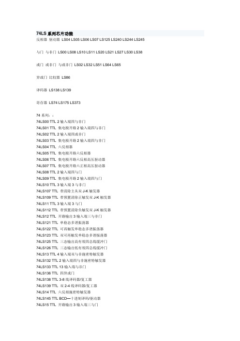
74LS系列芯片功能反相器驱动器LS04 LS05 LS06 LS07 LS125 LS240 LS244 LS245 与门与非门LS00 LS08 LS10 LS11 LS20 LS21 LS27 LS30 LS38 或门或非门与或非门LS02 LS32 LS51 LS64 LS65异或门比较器LS86译码器LS138 LS139寄存器LS74 LS175 LS37374系列::74LS00 TTL 2输入端四与非门74LS01 TTL 集电极开路2输入端四与非门74LS02 TTL 2输入端四或非门74LS03 TTL 集电极开路2输入端四与非门74LS04 TTL 六反相器74LS05 TTL 集电极开路六反相器74LS06 TTL 集电极开路六反相高压驱动器74LS07 TTL 集电极开路六正相高压驱动器74LS08 TTL 2输入端四与门74LS09 TTL 集电极开路2输入端四与门74LS10 TTL 3输入端3与非门74LS107 TTL 带清除主从双J-K触发器74LS109 TTL 带预置清除正触发双J-K触发器74LS11 TTL 3输入端3与门74LS112 TTL 带预置清除负触发双J-K触发器74LS12 TTL 开路输出3输入端三与非门74LS121 TTL 单稳态多谐振荡器74LS122 TTL 可再触发单稳态多谐振荡器74LS123 TTL 双可再触发单稳态多谐振荡器74LS125 TTL 三态输出高有效四总线缓冲门74LS126 TTL 三态输出低有效四总线缓冲门74LS13 TTL 4输入端双与非施密特触发器74LS132 TTL 2输入端四与非施密特触发器74LS133 TTL 13输入端与非门74LS136 TTL 四异或门74LS138 TTL 3-8线译码器/复工器74LS139 TTL 双2-4线译码器/复工器74LS14 TTL 六反相施密特触发器74LS145 TTL BCD—十进制译码/驱动器74LS15 TTL 开路输出3输入端三与门74LS150 TTL 16选1数据选择/多路开关74LS151 TTL 8选1数据选择器74LS153 TTL 双4选1数据选择器74LS154 TTL 4线—16线译码器74LS155 TTL 图腾柱输出译码器/分配器74LS156 TTL 开路输出译码器/分配器74LS157 TTL 同相输出四2选1数据选择器74LS158 TTL 反相输出四2选1数据选择器74LS16 TTL 开路输出六反相缓冲/驱动器74LS160 TTL 可预置BCD异步清除计数器74LS161 TTL 可予制四位二进制异步清除计数器74LS162 TTL 可预置BCD同步清除计数器74LS163 TTL 可予制四位二进制同步清除计数器74LS164 TTL 八位串行入/并行输出移位寄存器74LS165 TTL 八位并行入/串行输出移位寄存器74LS166 TTL 八位并入/串出移位寄存器74LS169 TTL 二进制四位加/减同步计数器74LS17 TTL 开路输出六同相缓冲/驱动器74LS170 TTL 开路输出4×4寄存器堆74LS173 TTL 三态输出四位D型寄存器74LS174 TTL 带公共时钟和复位六D触发器74LS175 TTL 带公共时钟和复位四D触发器74LS180 TTL 9位奇数/偶数发生器/校验器74LS181 TTL 算术逻辑单元/函数发生器74LS185 TTL 二进制—BCD代码转换器74LS190 TTL BCD同步加/减计数器74LS191 TTL 二进制同步可逆计数器74LS192 TTL 可预置BCD双时钟可逆计数器74LS193 TTL 可预置四位二进制双时钟可逆计数器74LS194 TTL 四位双向通用移位寄存器74LS195 TTL 四位并行通道移位寄存器74LS196 TTL 十进制/二-十进制可预置计数锁存器74LS197 TTL 二进制可预置锁存器/计数器74LS20 TTL 4输入端双与非门74LS21 TTL 4输入端双与门74LS22 TTL 开路输出4输入端双与非门74LS221 TTL 双/单稳态多谐振荡器74LS240 TTL 八反相三态缓冲器/线驱动器74LS241 TTL 八同相三态缓冲器/线驱动器74LS243 TTL 四同相三态总线收发器74LS244 TTL 八同相三态缓冲器/线驱动器74LS245 TTL 八同相三态总线收发器74LS247 TTL BCD—7段15V输出译码/驱动器74LS248 TTL BCD—7段译码/升压输出驱动器74LS249 TTL BCD—7段译码/开路输出驱动器74LS251 TTL 三态输出8选1数据选择器/复工器74LS253 TTL 三态输出双4选1数据选择器/复工器74LS256 TTL 双四位可寻址锁存器74LS257 TTL 三态原码四2选1数据选择器/复工器74LS258 TTL 三态反码四2选1数据选择器/复工器74LS259 TTL 八位可寻址锁存器/3-8线译码器74LS26 TTL 2输入端高压接口四与非门74LS260 TTL 5输入端双或非门74LS266 TTL 2输入端四异或非门74LS27 TTL 3输入端三或非门74LS273 TTL 带公共时钟复位八D触发器74LS279 TTL 四图腾柱输出S-R锁存器74LS28 TTL 2输入端四或非门缓冲器74LS283 TTL 4位二进制全加器74LS290 TTL 二/五分频十进制计数器74LS293 TTL 二/八分频四位二进制计数器74LS295 TTL 四位双向通用移位寄存器74LS298 TTL 四2输入多路带存贮开关74LS299 TTL 三态输出八位通用移位寄存器74LS30 TTL 8输入端与非门74LS32 TTL 2输入端四或门74LS322 TTL 带符号扩展端八位移位寄存器74LS323 TTL 三态输出八位双向移位/存贮寄存器74LS33 TTL 开路输出2输入端四或非缓冲器74LS347 TTL BCD—7段译码器/驱动器74LS352 TTL 双4选1数据选择器/复工器74LS353 TTL 三态输出双4选1数据选择器/复工器74LS365 TTL 门使能输入三态输出六同相线驱动器74LS365 TTL 门使能输入三态输出六同相线驱动器74LS366 TTL 门使能输入三态输出六反相线驱动器74LS367 TTL 4/2线使能输入三态六同相线驱动器74LS368 TTL 4/2线使能输入三态六反相线驱动器74LS37 TTL 开路输出2输入端四与非缓冲器74LS373 TTL 三态同相八D锁存器74LS374 TTL 三态反相八D锁存器74LS375 TTL 4位双稳态锁存器74LS377 TTL 单边输出公共使能八D锁存器74LS378 TTL 单边输出公共使能六D锁存器74LS379 TTL 双边输出公共使能四D锁存器74LS38 TTL 开路输出2输入端四与非缓冲器74LS380 TTL 多功能八进制寄存器74LS39 TTL 开路输出2输入端四与非缓冲器74LS390 TTL 双十进制计数器74LS393 TTL 双四位二进制计数器74LS40 TTL 4输入端双与非缓冲器74LS42 TTL BCD—十进制代码转换器74LS352 TTL 双4选1数据选择器/复工器74LS353 TTL 三态输出双4选1数据选择器/复工器74LS365 TTL 门使能输入三态输出六同相线驱动器74LS366 TTL 门使能输入三态输出六反相线驱动器74LS367 TTL 4/2线使能输入三态六同相线驱动器74LS368 TTL 4/2线使能输入三态六反相线驱动器74LS37 TTL 开路输出2输入端四与非缓冲器74LS373 TTL 三态同相八D锁存器74LS374 TTL 三态反相八D锁存器74LS375 TTL 4位双稳态锁存器74LS377 TTL 单边输出公共使能八D锁存器74LS378 TTL 单边输出公共使能六D锁存器74LS379 TTL 双边输出公共使能四D锁存器74LS38 TTL 开路输出2输入端四与非缓冲器74LS380 TTL 多功能八进制寄存器74LS39 TTL 开路输出2输入端四与非缓冲器74LS390 TTL 双十进制计数器74LS393 TTL 双四位二进制计数器74LS40 TTL 4输入端双与非缓冲器74LS42 TTL BCD—十进制代码转换器74LS447 TTL BCD—7段译码器/驱动器74LS45 TTL BCD—十进制代码转换/驱动器74LS450 TTL 16:1多路转接复用器多工器74LS451 TTL 双8:1多路转接复用器多工器74LS453 TTL 四4:1多路转接复用器多工器74LS46 TTL BCD—7段低有效译码/驱动器74LS460 TTL 十位比较器74LS461 TTL 八进制计数器74LS465 TTL 三态同相2与使能端八总线缓冲器74LS466 TTL 三态反相2与使能八总线缓冲器74LS467 TTL 三态同相2使能端八总线缓冲器74LS468 TTL 三态反相2使能端八总线缓冲器74LS469 TTL 八位双向计数器74LS47 TTL BCD—7段高有效译码/驱动器74LS48 TTL BCD—7段译码器/内部上拉输出驱动74LS490 TTL 双十进制计数器74LS491 TTL 十位计数器74LS498 TTL 八进制移位寄存器74LS50 TTL 2-3/2-2输入端双与或非门74LS502 TTL 八位逐次逼近寄存器74LS503 TTL 八位逐次逼近寄存器74LS51 TTL 2-3/2-2输入端双与或非门74LS533 TTL 三态反相八D锁存器74LS534 TTL 三态反相八D锁存器74LS54 TTL 四路输入与或非门74LS540 TTL 八位三态反相输出总线缓冲器74LS55 TTL 4输入端二路输入与或非门74LS563 TTL 八位三态反相输出触发器74LS564 TTL 八位三态反相输出D触发器74LS573 TTL 八位三态输出触发器74LS574 TTL 八位三态输出D触发器74LS645 TTL 三态输出八同相总线传送接收器74LS670 TTL 三态输出4×4寄存器堆74LS73 TTL 带清除负触发双J-K触发器74LS74 TTL 带置位复位正触发双D触发器74LS76 TTL 带预置清除双J-K触发器74LS83 TTL 四位二进制快速进位全加器74LS85 TTL 四位数字比较器74LS86 TTL 2输入端四异或门74LS90 TTL 可二/五分频十进制计数器74LS93 TTL 可二/八分频二进制计数器74LS95 TTL 四位并行输入\输出移位寄存器74LS97 TTL 6位同步二进制乘法器反相器:Vcc 6A 6Y 5A 5Y 4A 4Y 六非门74LS04┌┴—┴—┴—┴—┴—┴—┴┐ 六非门(OC门) 74LS05 _ │14 13 12 11 10 9 8│ 六非门(OC高压输出) 74LS06 Y = A )││ 1 2 3 4 5 6 7│└┬—┬—┬—┬—┬—┬—┬┘1A 1Y 2A 2Y 3A 3Y GND驱动器:Vcc 6A 6Y 5A 5Y 4A 4Y┌┴—┴—┴—┴—┴—┴—┴┐│14 13 12 11 10 9 8│Y = A )│ 六驱动器(OC高压输出) 74LS07│ 1 2 3 4 5 6 7│└┬—┬—┬—┬—┬—┬—┬┘1A 1Y 2A 2Y 3A 3Y GNDVcc -4C 4A 4Y -3C 3A 3Y┌┴—┴—┴—┴—┴—┴—┴┐_ │14 13 12 11 10 9 8│Y =A+C )│ 四总线三态门74LS125│ 1 2 3 4 5 6 7│└┬—┬—┬—┬—┬—┬—┬┘-1C 1A 1Y -2C 2A 2Y GNDVcc -G B1 B2 B3 B4 B8 B6 B7 B8┌┴—┴—┴—┴—┴—┴—┴—┴—┴—┴┐ 8位总线驱动器74LS245│20 19 18 17 16 15 14 13 12 11│)│ DIR=1 A=>B│ 1 2 3 4 5 6 7 8 9 10│ DIR=0 B=>A└┬—┬—┬—┬—┬—┬—┬—┬—┬—┬┘DIR A1 A2 A3 A4 A5 A6 A7 A8 GND页首非门,驱动器与门,与非门或门,或非门异或门,比较器译码器寄存器正逻辑与门,与非门:Vcc 4B 4A 4Y 3B 3A 3Y┌┴—┴—┴—┴—┴—┴—┴┐│14 13 12 11 10 9 8│Y = AB )│ 2输入四正与门74LS08│ 1 2 3 4 5 6 7│└┬—┬—┬—┬—┬—┬—┬┘1A 1B 1Y 2A 2B 2Y GNDVcc 4B 4A 4Y 3B 3A 3Y┌┴—┴—┴—┴—┴—┴—┴┐__ │14 13 12 11 10 9 8│Y = AB )│ 2输入四正与非门74LS00│ 1 2 3 4 5 6 7│└┬—┬—┬—┬—┬—┬—┬┘1A 1B 1Y 2A 2B 2Y GNDVcc 1C 1Y 3C 3B 3A 3Y┌┴—┴—┴—┴—┴—┴—┴┐___ │14 13 12 11 10 9 8│Y = ABC )│ 3输入三正与非门74LS10│ 1 2 3 4 5 6 7│└┬—┬—┬—┬—┬—┬—┬┘1A 1B 2A 2B 2C 2Y GNDVcc H G Y┌┴—┴—┴—┴—┴—┴—┴┐│14 13 12 11 10 9 8│)│ 8输入与非门74LS30│ 1 2 3 4 5 6 7│ ________└┬—┬—┬—┬—┬—┬—┬┘ Y = ABCDEFGHA B C D E F GND页首非门,驱动器与门,与非门或门,或非门异或门,比较器译码器寄存器正逻辑或门,或非门:Vcc 4B 4A 4Y 3B 3A 3Y┌┴—┴—┴—┴—┴—┴—┴┐ 2输入四或门74LS32│14 13 12 11 10 9 8│)│ Y = A+B│ 1 2 3 4 5 6 7│└┬—┬—┬—┬—┬—┬—┬┘1A 1B 1Y 2A 2B 2Y GNDVcc 4Y 4B 4A 3Y 3B 3A┌┴—┴—┴—┴—┴—┴—┴┐ 2输入四或非门74LS02│14 13 12 11 10 9 8│ ___)│ Y = A+B│ 1 2 3 4 5 6 7│└┬—┬—┬—┬—┬—┬—┬┘1Y 1A 1B 2Y 2A 2B GNDVcc 2Y 2B 2A 2D 2E 1F┌┴—┴—┴—┴—┴—┴—┴┐ 双与或非门74S51│14 13 12 11 10 9 8│ _____)│ 2Y = AB+DE│ 1 2 3 4 5 6 7│ _______└┬—┬—┬—┬—┬—┬—┬┘ 1Y = ABC+DEF1Y 1A 1B 1C 1D 1E GNDVcc D C B K J Y┌┴—┴—┴—┴—┴—┴—┴┐ 4-2-3-2与或非门74S64 74S65(OC门)│14 13 12 11 10 9 8│ ______________)│ Y = ABCD+EF+GHI+JK│ 1 2 3 4 5 6 7│└┬—┬—┬—┬—┬—┬—┬┘A E F G H I GND页首非门,驱动器与门,与非门或门,或非门异或门,比较器译码器寄存器2输入四异或门74LS86Vcc 4B 4A 4Y 3Y 3B 3A┌┴—┴—┴—┴—┴—┴—┴┐│14 13 12 11 10 9 8│)│ _ _│ 1 2 3 4 5 6 7│ Y=AB+AB└┬—┬—┬—┬—┬—┬—┬┘1A 1B 1Y 2Y 2A 2B GND8*2输入比较器74LS688_Vcc Y B8 A8 B7 A7 B6 A6 B5 A5┌┴—┴—┴—┴—┴—┴—┴—┴—┴—┴┐ 8*2输入比较器74LS688│20 19 18 17 16 15 14 13 12 11│)││ 1 2 3 4 5 6 7 8 9 10│└┬—┬—┬—┬—┬—┬—┬—┬—┬—┬┘CE A1 B1 A2 B2 A3 B3 A4 B4 GND_Y=A1⊙B1+A2⊙B2+A3⊙B3+A4⊙B4+A5⊙B5+A6⊙B6+A7⊙B7+A8⊙B8 页首非门,驱动器与门,与非门或门,或非门异或门,比较器译码器寄存器3-8译码器74LS138Vcc -Y0 -Y1 -Y2 -Y3 -Y4 -Y5 -Y6 __ _ _ _ __ _ _ __ _ _ __ _┌┴—┴—┴—┴—┴—┴—┴—┴┐ Y0=A B C Y1=A B B Y2=A B C Y3=A B C │16 15 14 13 12 11 10 9 │)│ __ _ _ __ _ __ _ __│ 1 2 3 4 5 6 78│ Y4=A B C Y5=A B C Y6=A B C Y7=A B C└┬—┬—┬—┬—┬—┬—┬—┬┘A B C -CS0 -CS1 CS2 -Y7 GND双2-4译码器74LS139Vcc -2G 2A 2B -Y0 -Y1 -Y2 -Y3 __ __ __ __ __ __ __ __┌┴—┴—┴—┴—┴—┴—┴—┴┐ Y0=2A 2B Y1=2A 2B Y2=2A 2B Y3=2A 2B │16 15 14 13 12 11 10 9 │)│ __ __ __ __ __ __ __ __│ 1 2 3 4 5 6 7 8│ Y0=1A 1B Y1=1A 1B Y2=1A 1B Y3=1A 1B└┬—┬—┬—┬—┬—┬—┬—┬┘-1G 1A 1B -Y0 -Y1 -Y2 -Y3 GND8*2输入比较器74LS688_Vcc Y B8 A8 B7 A7 B6 A6 B5 A5┌┴—┴—┴—┴—┴—┴—┴—┴—┴—┴┐ 8*2输入比较器74LS688│20 19 18 17 16 15 14 13 12 11│)││ 1 2 3 4 5 6 7 8 9 10│└┬—┬—┬—┬—┬—┬—┬—┬—┬—┬┘CE A1 B1 A2 B2 A3 B3 A4 B4 GND_Y=A1⊙B1+A2⊙B2+A3⊙B3+A4⊙B4+A5⊙B5+A6⊙B6+A7⊙B7+A8⊙B8寄存器:Vcc 2CR 2D 2Ck 2St 2Q -2Q┌┴—┴—┴—┴—┴—┴—┴┐ 双D触发器74LS74│14 13 12 11 10 9 8 │)││ 1 2 3 4 5 6 7│└┬—┬—┬—┬—┬—┬—┬┘1Cr 1D 1Ck 1St 1Q -1Q GNDVcc 8Q 8D 7D 7Q 6Q 6D 5D 5Q ALE┌┴—┴—┴—┴—┴—┴—┴—┴—┴—┴┐ 8位锁存器74LS373│20 19 18 17 16 15 14 13 12 11│)││ 1 2 3 4 5 6 7 8 9 10│└┬—┬—┬—┬—┬—┬—┬—┬—┬—┬┘-OE 1Q 1D 2D 2Q 3Q 3D 4D 4Q GND74HC系列功能表集成电路-74HC系列型号器件名称厂牌[数据表] 74HC00 四2输入端与非门 TI74HC01 四2输入端与非门(OC)74HC02 四2输入端或非门 TI74HC03 四2输入端与非门(OC) TI74HC04 六反相器 TI74HC05 HEX INVERTERS74HC08 四2输入端与门 TI74HC09 QUADRUPLE 2-INPUT POSITIVE-AND74HC10 三3输入端与非门 TI74HC11 三3输入端与门 TI74HC14 双4输入端与非门 TI74HC20 双4输入端与非门 TI74HC21 双4输入端与门 TI74HC27 三3输入端或非门 TI74HC30 8输入端与非门 TI74HC32 四2输入端或门 TI74HC42 4线-10线译码器(BCD输入) TI74HC73 DUAL J-K FLIP-FLOP TI74HC74 双上升沿D型触发器 TI74HC75 4-BIT BISTABLE LATCH TI74HC85A 四位数值比较器 TI74HC86 四2输入端异或门 TI74HC93 双4输入端与非门 TI74HC107 双主-从J-K触发器 TI74HC109 双J-K触发器 TI74HC112 双下降沿J-K触发器 TI型号器件名称厂牌[数据表]74HC123 可重触发双稳态触发器 TI74HC125 四总线缓冲器 TI74HC126 四总线缓冲器74HC132 四2输入端与非门74HC133 13-INPUT POSITIVE-NAND74HC137 地址锁存3线-8线译码器74HC138 3线-8线译码器74HC139 双2线-4线译码器74HC147 10线-4线优先编码器74HC148 8-LINE TO 3-LINE PRIORITY ENCODERS74HC151 8-INPUT MULTIPLEXER74HC153 DUAL 4-INPUT MULTIPLEXER74HC154 4线-16线译码器74HC157 四2选1数据选择器74HC158 四2选1数据选择器74HC160 DECADE COUNTER74HC161 4位二进制同步计数器74HC162 DECADE COUNTER74HC163 4-BIT BINARY PRESETTABLE COUNTER74HC164 8位移位寄存器74HC165 8位并行输入/串行输出寄存器74HC166 8位并行输入/串行输出移位寄存器 TI,PHI 74HC173 4位D型寄存器 TI74HC174 HEX D-TYPE FLIP-FLOP WITH RESET TI74HC175 四上升沿D型触发器 TI74HC190 十进制同步加/减计数器 TI74HC191 4位二进制同步加/减计数器 TI74HC192 BCD二进制同步加/减计数器 TI型号器件名称厂牌[数据表]74HC193 可预置4位二进制加/减计数器 TI74HC194 4位并入/串入-并出/串出移位寄存 TI74HC195 4位移位寄存器 TI74HC221 双单稳态触器 TI74HC237 3-8线译码器(带地址锁存) TI74HC238 3-8线译码器 TI74HC239 双2-4线译码器74HC240 八反相缓冲/线驱动/线接收器 TI74HC241 八缓冲/线驱动/线接收器 TI74HC243 四总线收发器 TI74HC244 八缓冲/线驱动/线接收器 TI,FSC74HC245 八双向总线发送/接发器 TI,FSC74HC251 8选1数据选择器74HC253 双4选1数据选择器74HC257 四2选1数据选择器74HC258 四2选1数据选择器74HC259 8位可寻址锁存器74HC266 QUADRUPLE 2-INPUT EXCLUSIVE-NOR74HC273 八D触发器74HC280 9位奇偶产生器/校验器 TI74HC283 4位二进制超位全加器74HC297 DIGITAL PHASE-LOCKED-LOOP74HC299 8位双向通用移位/存储寄存器型号器件名称厂牌[数据表]74HC354 带锁存三态8-1多路转换开关74HC365 六总线驱动器74HC366 六反相总线驱动器74HC367 六总线驱动器74HC368 六反相总线驱动器74HC373 六D型锁存器74HC374 六上升沿D型触发器74HC375 4-BIT BISTABLE LATCH74HC377 六上升沿D型触发器74HC378 6-BIT D-TYPE FLIP-FLOP74HC379 QUADRUPLE D-TYPE FLIP-FLOP74HC390 双十进制计数器74HC393 双4位二进制计数器74HC4002 高速CMOS双4输入端或非门74HC4015 高速CMOS双4位串入/并出移位寄存器74HC4016 高速CMOS四传输门74HC4017 高速CMOS十进制计数/分配器74HC4020 高速CMOS14级串行二进制计数/分频器74HC4024 高速CMOS7级二进制串行计数/分频器74HC4040 高速CMOS12级二进制串行计数/分频器74HC4046A 高速CMOS锁相环74HC4049 高速CMOS六反相缓冲/变换器74HC4050 高速CMOS六同相缓冲/变换器CD系列芯片功能CD4000 双3输入端或非门+单非门TICD4001 四2输入端或非门HIT/NSC/TI/GOLCD4002 双4输入端或非门NSCCD4006 18位串入/串出移位寄存器NSCCD4007 双互补对加反相器NSCCD4008 4位超前进位全加器NSCCD4009 六反相缓冲/变换器NSCCD4010 六同相缓冲/变换器NSCCD4011 四2输入端与非门HIT/TICD4012 双4输入端与非门NSCCD4013 双主-从D型触发器FSC/NSC/TOSCD4014 8位串入/并入-串出移位寄存器NSCCD4015 双4位串入/并出移位寄存器TICD4016 四传输门FSC/TICD4017 十进制计数/分配器FSC/TI/MOTCD4018 可预制1/N计数器NSC/MOTCD4019 四与或选择器PHICD4020 14级串行二进制计数/分频器FSCCD4021 08位串入/并入-串出移位寄存器PHI/NSCCD4022 八进制计数/分配器NSC/MOTCD4023 三3输入端与非门NSC/MOT/TICD4024 7级二进制串行计数/分频器NSC/MOT/TICD4025 三3输入端或非门NSC/MOT/TICD4026 十进制计数/7段译码器NSC/MOT/TICD4027 双J-K触发器NSC/MOT/TICD4028 BCD码十进制译码器NSC/MOT/TICD4029 可预置可逆计数器NSC/MOT/TICD4030 四异或门NSC/MOT/TI/GOLCD4031 64位串入/串出移位存储器NSC/MOT/TICD4032 三串行加法器NSC/TICD4033 十进制计数/7段译码器NSC/TICD4034 8位通用总线寄存器NSC/MOT/TICD4035 4位并入/串入-并出/串出移位寄存NSC/MOT/TI CD4038 三串行加法器NSC/TICD4040 12级二进制串行计数/分频器NSC/MOT/TICD4041 四同相/反相缓冲器NSC/MOT/TICD4042 四锁存D型触发器NSC/MOT/TICD4043 4三态R-S锁存触发器("1"触发) NSC/MOT/TI CD4044 四三态R-S锁存触发器("0"触发) NSC/MOT/TI CD4046 锁相环NSC/MOT/TI/PHICD4047 无稳态/单稳态多谐振荡器NSC/MOT/TICD4048 4输入端可扩展多功能门NSC/HIT/TICD4049 六反相缓冲/变换器NSC/HIT/TICD4050 六同相缓冲/变换器NSC/MOT/TICD4051 八选一模拟开关NSC/MOT/TICD4052 双4选1模拟开关NSC/MOT/TICD4053 三组二路模拟开关NSC/MOT/TICD4054 液晶显示驱动器NSC/HIT/TICD4055 BCD-7段译码/液晶驱动器NSC/HIT/TI CD4056 液晶显示驱动器NSC/HIT/TICD4059 “N”分频计数器NSC/TICD4060 14级二进制串行计数/分频器NSC/TI/MOT CD4063 四位数字比较器NSC/HIT/TICD4066 四传输门NSC/TI/MOTCD4067 16选1模拟开关NSC/TICD4068 八输入端与非门/与门NSC/HIT/TICD4069 六反相器NSC/HIT/TICD4070 四异或门NSC/HIT/TICD4071 四2输入端或门NSC/TICD4072 双4输入端或门NSC/TICD4073 三3输入端与门NSC/TICD4075 三3输入端或门NSC/TICD4076 四D寄存器CD4077 四2输入端异或非门HITCD4078 8输入端或非门/或门CD4081 四2输入端与门NSC/HIT/TICD4082 双4输入端与门NSC/HIT/TICD4085 双2路2输入端与或非门CD4086 四2输入端可扩展与或非门CD4089 二进制比例乘法器CD4093 四2输入端施密特触发器NSC/MOT/ST CD4094 8位移位存储总线寄存器NSC/TI/PHICD4095 3输入端J-K触发器CD4096 3输入端J-K触发器CD4097 双路八选一模拟开关CD4098 双单稳态触发器NSC/MOT/TICD4099 8位可寻址锁存器NSC/MOT/STCD40100 32位左/右移位寄存器CD40101 9位奇偶较验器CD40102 8位可预置同步BCD减法计数器CD40103 8位可预置同步二进制减法计数器CD40104 4位双向移位寄存器CD40105 先入先出FI-FD寄存器CD40106 六施密特触发器NSC\TICD40107 双2输入端与非缓冲/驱动器HAR\TICD40108 4字×4位多通道寄存器CD40109 四低-高电平位移器CD40110 十进制加/减,计数,锁存,译码驱动STCD40147 10-4线编码器NSC\MOTCD40160 可预置BCD加计数器NSC\MOTCD40161 可预置4位二进制加计数器NSC\MOTCD40162 BCD加法计数器NSC\MOTCD40163 4位二进制同步计数器NSC\MOTCD40174 六锁存D型触发器NSC\TI\MOTCD40175 四D型触发器NSC\TI\MOTCD40181 4位算术逻辑单元/函数发生器CD40182 超前位发生器CD40192 可预置BCD加/减计数器(双时钟) NSC\TI CD40193 可预置4位二进制加/减计数器NSC\TICD40194 4位并入/串入-并出/串出移位寄存NSC\MOT CD40195 4位并入/串入-并出/串出移位寄存NSC\MOT CD40208 4×4多端口寄存器型号器件名称厂牌备注CD4501 4输入端双与门及2输入端或非门CD4502 可选通三态输出六反相/缓冲器CD4503 六同相三态缓冲器CD4504 六电压转换器CD4506 双二组2输入可扩展或非门CD4508 双4位锁存D型触发器CD4510 可预置BCD码加/减计数器CD4511 BCD锁存,7段译码,驱动器CD4512 八路数据选择器CD4513 BCD锁存,7段译码,驱动器(消隐)CD4514 4位锁存,4线-16线译码器CD4515 4位锁存,4线-16线译码器CD4516 可预置4位二进制加/减计数器CD4517 双64位静态移位寄存器CD4518 双BCD同步加计数器CD4519 四位与或选择器CD4520 双4位二进制同步加计数器CD4521 24级分频器CD4522 可预置BCD同步1/N计数器CD4526 可预置4位二进制同步1/N计数器CD4527 BCD比例乘法器CD4528 双单稳态触发器CD4529 双四路/单八路模拟开关CD4530 双5输入端优势逻辑门CD4531 12位奇偶校验器CD4532 8位优先编码器CD4536 可编程定时器CD4538 精密双单稳CD4539 双四路数据选择器CD4541 可编程序振荡/计时器CD4543 BCD七段锁存译码,驱动器CD4544 BCD七段锁存译码,驱动器CD4547 BCD七段译码/大电流驱动器CD4549 函数近似寄存器CD4551 四2通道模拟开关CD4553 三位BCD计数器CD4555 双二进制四选一译码器/分离器CD4556 双二进制四选一译码器/分离器CD4558 BCD八段译码器CD4560 "N"BCD加法器CD4561 "9"求补器CD4573 四可编程运算放大器CD4574 四可编程电压比较器CD4575 双可编程运放/比较器CD4583 双施密特触发器CD4584 六施密特触发器CD4585 4位数值比较器CD4599 8位可寻址锁存器。
CD74HC259中文资料

[ /Title (CD74 HC259 , CD74 HCT25 9) /Subject (High Speed CMOS Logic 8-Bit Addres sable Latch)
Features
Description
• Buffered Inputs and Outputs
• Four Operating Modes
•
Typical Propagation Delay CL = 15pF, TA = 25oC
of
15ns
at
VCC
=
5V,
• Fanout (Over Temperature Range)
- Standard Outputs . . . . . . . . . . . . . . . 10 LSTTL Loads
The Harris CD74HC259 and CD74HCT259 Addressable Latch features the low-power consumption associated with CMOS circuitry and has speeds comparable to low-power Schottky.
115
Maximum Junction Temperature . . . . . . . . . . . . . . . . . . . . . . . 150oC
Maximum Storage Temperature Range . . . . . . . . . .-65oC to 150oC
2. Wafer or die for this part number is available which meets all electrical specifications. Please contact your local sales office or Harris customer service for ordering information.
74HC245详细中文资料

74HC245详细中文资料74HC245是一款高速CMOS器件,74HC2 45引脚兼容低功耗肖特基TTL(LSTTL)系列。
74HC245译码器可接受3位二进制加权地址输入(A0, A1和A2),并当使能时,提供8个互斥的低有效输出(Y0至Y7)。
74HC245特有3个使能输入端:两个低有效(E1和E2)和一个高有效(E3)。
除非E1和E2置低且E3置高,否则74HC138将保持所有输出为高。
利用这种复合使能特性,仅需4片7 4HC245芯片和1个反相器,即可轻松实现并行扩展,组合成为一个1-32(5线到32线)译码器。
任选一个低有效使能输入端作为数据输入,而把其余的使能输入端作为选通端,则74HC245亦可充当一个8输出多路分配器,未使用的使能输入端必须保持绑定在各自合适的高有效或低有效状态。
74HC245与74HC 238逻辑功能一致,只不过74HC138为反相输出。
功能CD74HC245 ,CD74HC238和CD74HCT245, CD74HCT238是高速硅栅CMO S解码器,适合内存地址解码或数据路由应用。
74HC245作用原理于高性能的存贮译码或要求传输延迟时间短的数据传输系统,在高性能存贮器系统中,用这种译码器可以提高译码系统的效率。
将快速赋能电路用于高速存贮器时,译码器的延迟时间和存贮器的赋能时间通常小于存贮器的典型存取时间,这就是说由肖特基钳位的系统译码器所引起的有效系统延迟可以忽略不计。
HC138 按照三位二进制输入码和赋能输入条件,从8 个输出端中译出一个低电平输出。
两个低电平有效的赋能输入端和一个高电平有效的赋能输入端减少了扩展所需要的外接门或倒相器,扩展成24 线译码器不需外接门;扩展成32 线译码器,只需要接一个外接倒相器。
在解调器应用中,赋能输入端可用作数据输入端。
特性复合使能输入,轻松实现扩展兼容JEDEC标准no.7A 存储器芯片译码选择的理想选择低有效互斥输出 ESD保护 HBM EIA/JESD22-A114-C超过2000 V MM EIA/JESD22-A115-A超过200 V 温度范围 -40~+85 ℃ -40~+125 ℃多路分配功能74HC245是一款高速CMOS器件,74HC245引脚兼容低功耗肖特基T TL(LSTTL)系列。
- 1、下载文档前请自行甄别文档内容的完整性,平台不提供额外的编辑、内容补充、找答案等附加服务。
- 2、"仅部分预览"的文档,不可在线预览部分如存在完整性等问题,可反馈申请退款(可完整预览的文档不适用该条件!)。
- 3、如文档侵犯您的权益,请联系客服反馈,我们会尽快为您处理(人工客服工作时间:9:00-18:30)。
PACKAGING INFORMATIONOrderable Device Status (1)Package Type Package DrawingPins Package Qty Eco Plan (2)Lead/Ball Finish MSL Peak Temp (3)5962-8970801EA ACTIVE CDIP J 161TBD A42SNPB N /A for Pkg Type CD54HCT258F3A ACTIVE CDIP J 161TBD A42SNPB N /A for Pkg Type CD74HCT258E ACTIVE PDIP N 1625Pb-Free (RoHS)CU NIPDAU N /A for Pkg Type CD74HCT258EE4ACTIVEPDIPN1625Pb-Free (RoHS)CU NIPDAUN /A for Pkg Type(1)The marketing status values are defined as follows:ACTIVE:Product device recommended for new designs.LIFEBUY:TI has announced that the device will be discontinued,and a lifetime-buy period is in effect.NRND:Not recommended for new designs.Device is in production to support existing customers,but TI does not recommend using this part in a new design.PREVIEW:Device has been announced but is not in production.Samples may or may not be available.OBSOLETE:TI has discontinued the production of the device.(2)Eco Plan -The planned eco-friendly classification:Pb-Free (RoHS),Pb-Free (RoHS Exempt),or Green (RoHS &no Sb/Br)-please check /productcontent for the latest availability information and additional product content details.TBD:The Pb-Free/Green conversion plan has not been defined.Pb-Free (RoHS):TI's terms "Lead-Free"or "Pb-Free"mean semiconductor products that are compatible with the current RoHS requirements for all 6substances,including the requirement that lead not exceed 0.1%by weight in homogeneous materials.Where designed to be soldered at high temperatures,TI Pb-Free products are suitable for use in specified lead-free processes.Pb-Free (RoHS Exempt):This component has a RoHS exemption for either 1)lead-based flip-chip solder bumps used between the die and package,or 2)lead-based die adhesive used between the die and leadframe.The component is otherwise considered Pb-Free (RoHS compatible)as defined above.Green (RoHS &no Sb/Br):TI defines "Green"to mean Pb-Free (RoHS compatible),and free of Bromine (Br)and Antimony (Sb)based flame retardants (Br or Sb do not exceed 0.1%by weight in homogeneous material)(3)MSL,Peak Temp.--The Moisture Sensitivity Level rating according to the JEDEC industry standard classifications,and peak solder temperature.Important Information and Disclaimer:The information provided on this page represents TI's knowledge and belief as of the date that it is provided.TI bases its knowledgeand belief on information provided by third parties,and makes no representation or warranty as to the accuracy of such information.Efforts are underway to better integrate information from third parties.TI has taken and continues to take reasonable steps to provide representative and accurate information but may not have conducted destructive testing or chemical analysis on incoming materials and chemicals.TI and TI suppliers consider certain information to be proprietary,and thus CAS numbers and other limited information may not be available for release.In no event shall TI's liability arising out of such information exceed the total purchase price of the TI part(s)at issue in this document sold by TI to Customer on an annual basis.PACKAGE OPTION ADDENDUM18-Sep-2008Addendum-Page 1IMPORTANT NOTICETexas Instruments Incorporated and its subsidiaries(TI)reserve the right to make corrections,modifications,enhancements,improvements, and other changes to its products and services at any time and to discontinue any product or service without notice.Customers should obtain the latest relevant information before placing orders and should verify that such information is current and complete.All products are sold subject to TI’s terms and conditions of sale supplied at the time of order acknowledgment.TI warrants performance of its hardware products to the specifications applicable at the time of sale in accordance with TI’s standard warranty.Testing and other quality control techniques are used to the extent TI deems necessary to support this warranty.Except where mandated by government requirements,testing of all parameters of each product is not necessarily performed.TI assumes no liability for applications assistance or customer product design.Customers are responsible for their products and applications using TI components.To minimize the risks associated with customer products and applications,customers should provide adequate design and operating safeguards.TI does not warrant or represent that any license,either express or implied,is granted under any TI patent right,copyright,mask work right, or other TI intellectual property right relating to any combination,machine,or process in which TI products or services are rmation published by TI regarding third-party products or services does not constitute a license from TI to use such products or services or a warranty or endorsement e of such information may require a license from a third party under the patents or other intellectual property of the third party,or a license from TI under the patents or other intellectual property of TI.Reproduction of TI information in TI data books or data sheets is permissible only if reproduction is without alteration and is accompanied by all associated warranties,conditions,limitations,and notices.Reproduction of this information with alteration is an unfair and deceptive business practice.TI is not responsible or liable for such altered rmation of third parties may be subject to additional restrictions.Resale of TI products or services with statements different from or beyond the parameters stated by TI for that product or service voids all express and any implied warranties for the associated TI product or service and is an unfair and deceptive business practice.TI is not responsible or liable for any such statements.TI products are not authorized for use in safety-critical applications(such as life support)where a failure of the TI product would reasonably be expected to cause severe personal injury or death,unless officers of the parties have executed an agreement specifically governing such use.Buyers represent that they have all necessary expertise in the safety and regulatory ramifications of their applications,and acknowledge and agree that they are solely responsible for all legal,regulatory and safety-related requirements concerning their products and any use of TI products in such safety-critical applications,notwithstanding any applications-related information or support that may be provided by TI.Further,Buyers must fully indemnify TI and its representatives against any damages arising out of the use of TI products in such safety-critical applications.TI products are neither designed nor intended for use in military/aerospace applications or environments unless the TI products are specifically designated by TI as military-grade or"enhanced plastic."Only products designated by TI as military-grade meet military specifications.Buyers acknowledge and agree that any such use of TI products which TI has not designated as military-grade is solely at the Buyer's risk,and that they are solely responsible for compliance with all legal and regulatory requirements in connection with such use. TI products are neither designed nor intended for use in automotive applications or environments unless the specific TI products are designated by TI as compliant with ISO/TS16949requirements.Buyers acknowledge and agree that,if they use any non-designated products in automotive applications,TI will not be responsible for any failure to meet such requirements.Following are URLs where you can obtain information on other Texas Instruments products and application solutions:Products ApplicationsAmplifiers AudioData Converters AutomotiveDSP BroadbandClocks and Timers Digital ControlInterface MedicalLogic MilitaryPower Mgmt Optical NetworkingMicrocontrollers SecurityRFID TelephonyRF/IF and ZigBee®Solutions Video&ImagingWirelessMailing Address:Texas Instruments,Post Office Box655303,Dallas,Texas75265Copyright©2008,Texas Instruments Incorporated。