MAX5123BEEE+中文资料
MAX3444EESA+中文资料

General DescriptionThe MAX3440E–MAX3444E fault-protected RS-485 and J1708 transceivers feature ±60V protection from signal faults on communication bus lines. Each device contains one differential line driver with three-state output and one differential line receiver with three-state input. The 1/4-unit-load receiver input impedance allows up to 128 trans-ceivers on a single bus. The devices operate from a 5V supply at data rates of up to 10Mbps. True fail-safe inputs guarantee a logic-high receiver output when the receiver inputs are open, shorted, or connected to an idle data line.Hot-swap circuitry eliminates false transitions on the data bus during circuit initialization or connection to a live backplane. Short-circuit current-limiting and ther-mal shutdown circuitry protect the driver against exces-sive power dissipation, and on-chip ±15kV ESD protection eliminates costly external protection devices.The MAX3440E–MAX3444E are available in 8-pin SO and PDIP packages and are specified over industrial and automotive temperature ranges.ApplicationsRS-422/RS-485 Communications Truck and Trailer Applications Industrial NetworksTelecommunications Systems Automotive Applications Features♦±15kV ESD Protection ♦±60V Fault Protection♦Guaranteed 10Mbps Data Rate (MAX3441E/MAX3443E)♦Hot Swappable for Telecom Applications ♦True Fail-Safe Receiver Inputs♦Enhanced Slew-Rate-Limiting Facilitates Error-Free Data Transmission(MAX3440E/MAX3442E/MAX3444E)♦Allow Up to 128 Transceivers on the Bus ♦-7V to +12V Common-Mode Input Range♦Automotive Temperature Range (-40°C to +125°C)♦Industry-Standard PinoutMAX3440E–MAX3444E±15kV ESD-Protected, ±60V Fault-Protected,10Mbps, Fail-Safe RS-485/J1708 Transceivers________________________________________________________________Maxim Integrated Products 1Pin Configurations and Typical Operating CircuitsOrdering Information19-2666; Rev 1; 12/05For pricing, delivery, and ordering information, please contact Maxim Direct at 1-888-629-4642,or visit Maxim’s website at .Ordering Information continued at end of data sheet.M A X 3440E –M A X 3444E±15kV ESD-Protected, ±60V Fault-Protected,10Mbps, Fail-Safe RS-485/J1708 Transceivers 2_______________________________________________________________________________________ABSOLUTE MAXIMUM RATINGSStresses beyond those listed under “Absolute Maximum Ratings” may cause permanent damage to the device. These are stress ratings only, and functional operation of the device at these or any other conditions beyond those indicated in the operational sections of the specifications is not implied. Exposure to absolute maximum rating conditions for extended periods may affect device reliability.Voltages Referenced to GNDV CC ........................................................................................+7V FAULT, DE/RE, RE , DE, DE , DI, TXD..........-0.3V to (V CC + 0.3V)A, B (Note 1)........................................................................±60V RO..............................................................-0.3V to (V CC + 0.3V)Short-Circuit Duration (RO, A, B)...............................Continuous Continuous Power Dissipation (T A = +70°C)8-Pin SO (derate 5.9mW/°C above +70°C)..................471mW 8-Pin PDIP (derate 9.09mW/°C above +70°C).............727mWOperating Temperature RangesMAX344_EE_ _...............................................-40°C to +85°C MAX344_EA_ _.............................................-40°C to +125°C Storage Temperature Range.............................-65°C to +150°C Junction Temperature......................................................+150°C Lead Temperature (soldering, 10s).................................+300°CDC ELECTRICAL CHARACTERISTICSNote 1:A, B must be terminated with 54Ωor 100Ωto guarantee ±60V fault protection.MAX3440E–MAX3444E±15kV ESD-Protected, ±60V Fault-Protected,10Mbps, Fail-Safe RS-485/J1708 TransceiversDC ELECTRICAL CHARACTERISTICS (continued)(V = +4.75V to +5.25V, T = T to T , unless otherwise noted. Typical values are at V = +5V and T = +25°C.)M A X 3440E –M A X 3444E±15kV ESD-Protected, ±60V Fault-Protected,10Mbps, Fail-Safe RS-485/J1708 Transceivers 4_______________________________________________________________________________________SWITCHING CHARACTERISTICS (MAX3440E/MAX3442E/MAX3444E)MAX3440E–MAX3444E±15kV ESD-Protected, ±60V Fault-Protected,10Mbps, Fail-Safe RS-485/J1708 Transceivers_______________________________________________________________________________________5SWITCHING CHARACTERISTICS (MAX3441E/MAX3443E)(V CC = +4.75V to +5.25V, T A = T MIN to T MAX , unless otherwise noted. Typical values are at V CC = +5V and T A = +25°C.)Note 3:The short-circuit output current applies to peak current just before foldback current limiting; the short-circuit foldback outputcurrent applies during current limiting to allow a recovery from bus contention.M A X 3440E –M A X 3444E±15kV ESD-Protected, ±60V Fault-Protected,10Mbps, Fail-Safe RS-485/J1708 Transceivers 6_______________________________________________________________________________________RECEIVER OUTPUT CURRENT vs. OUTPUT LOW VOLTAGEM A X 3443E t o c 04OUTPUT LOW VOLTAGE (V)R E C E I V E R O U T P U T C U R R E N T (m A )5.04.50.5 1.0 1.5 2.5 3.0 3.52.0 4.051015202530354000RECEIVER OUTPUT CURRENT vs. OUTPUT HIGH VOLTAGEM A X 3443E t o c 05OUTPUT HIGH VOLTAGE (V)R E C E I V E R O U T P U T C U R R E N T (m A )5.04.50.5 1.0 1.5 2.5 3.0 3.52.0 4.051015202530354000RECEIVER OUTPUT VOLTAGEvs. TEMPERATURETEMPERATURE (°C)R E C E I V E R O U T P U T V O L T A G E (V )110956580-105203550-250.51.01.52.02.53.03.54.04.55.0-40125DRIVER OUTPUT CURRENTvs. DIFFERENTIAL OUTPUT VOLTAGEDIFFERENTIAL OUTPUT VOLTAGE (V A - V B ) (V)D R I VE R O U T P U T C U R R E N T (m A )0.51.0 1.52.53.0 3.52.010203040506070800DIFFERENTIAL OUTPUT VOLTAGEvs. TEMPERATURETEMPERATURE (°C)D I F FE R E N T I A L O U T P U T V O L T A G E (V )110956580-105203550-250.51.01.52.02.53.03.50-40125Typical Operating Characteristics(V CC = +5V, T A = +25°C, unless otherwise noted.)NO-LOAD SUPPLY CURRENTvs. TEMPERATURETEMPERATURE (°C)S U P P L Y C U R R E N T (m A )1109580655035205-10-251234560-40125NO-LOAD SUPPLY CURRENTvs. TEMPERATURETEMPERATURE (°C)S U P P L Y C U R R E N T (m A )1109580655035205-10-2548121620240-40125SHUTDOWN SUPPLY CURRENTvs. TEMPERATURETEMPERATURE (°C)S U P P L Y C U R R E N T (μA )1109580655035205-10-250.11100.01-40125A, B CURRENTvs. A, B VOLTAGE (TO GROUND)A, B VOLTAGE (V)A ,BC U R R E N T (μA )40306050-50-40-30-10010-2020-800-400-1600-2000-12000400800120016002000-60MAX3440E–MAX3444E±15kV ESD-Protected, ±60V Fault-Protected,10Mbps, Fail-Safe RS-485/J1708 TransceiversOD OCFigure 3. Driver Propagation TimesTest Circuits and WaveformsM A X 3440E –M A X 3444E±15kV ESD-Protected, ±60V Fault-Protected,10Mbps, Fail-Safe RS-485/J1708 Transceivers 8_______________________________________________________________________________________Figure 7. Receiver Propagation DelayFigure 5. Driver Enable and Disable TimesMAX3440E–MAX3444E±15kV ESD-Protected, ±60V Fault-Protected,10Mbps, Fail-Safe RS-485/J1708 Transceivers_______________________________________________________________________________________9Note 4:The input pulse is supplied by a generator with the following characteristics: f = 5MHz, 50% duty cycle; tr ≤6ns; Z 0= 50Ω.Note 5:C L includes probe and stray capacitance.M A X 3440E –M A X 3444E±15kV ESD-Protected, ±60V Fault-Protected,10Mbps, Fail-Safe RS-485/J1708 Transceivers 10______________________________________________________________________________________MAX3440E–MAX3444E±15kV ESD-Protected, ±60V Fault-Protected,10Mbps, Fail-Safe RS-485/J1708 Transceivers______________________________________________________________________________________11Table 5. MAX3440E/MAX3441E (RS-485/RS-422)Detailed DescriptionThe MAX3440E–MAX3444E fault-protected transceivers for RS-485/RS-422 and J1708 communication contain one driver and one receiver. These devices feature fail-safe circuitry, which guarantees a logic-high receiver output when the receiver inputs are open or shorted, or when they are connected to a terminated transmission line with all drivers disabled (see the True Fail-Safe section). All devices have a hot-swap input structure that prevents disturbances on the differential signal lines when a circuit board is plugged into a hot back-plane (see the Hot-Swap Capability section). The MAX3440E/MAX3442E/MAX3444E feature a reduced slew-rate driver that minimizes EMI and reduces reflec-tions caused by improperly terminated cables, allowing error-free data transmission up to 250kbps (see the Reduced EMI and Reflections section). The MAX3441E/MAX3443E drivers are not slew-rate limited, allowing transmit speeds up to 10Mbps.DriverThe driver accepts a single-ended, logic-level input (DI) and transfers it to a differential, RS-485/RS-422level output (A and B). Deasserting the driver enable places the driver outputs (A and B) into a high-imped-ance state.ReceiverThe receiver accepts a differential, RS-485/RS-422level input (A and B), and transfers it to a single-ended,logic-level output (RO). Deasserting the receiver enable places the receiver inputs (A and B) into a high-imped-ance state (see Tables 1–7).Low-Power Shutdown(MAX3442E/MAX3443E/MAX3444E)The MAX3442E/MAX3443E/MAX3444E offer a low-power shutdown mode. Force DE low and RE high to shut down the MAX3442E/MAX3443E. Force DE and RE high to shut down the MAX3444E. A time delay of 50ns prevents the device from accidentally entering shutdown due to logic skews when switching between transmit and receive modes. Holding DE low and RE high for at least 800ns guarantees that the MAX3442E/MAX3443E enter shutdown. In shutdown, the devices consume a maxi-mum 20µA supply current.±60V Fault ProtectionThe driver outputs/receiver inputs of RS-485 devices in industrial network applications often experience voltage faults resulting from shorts to the power grid that exceed the -7V to +12V range specified in the EIA/TIA-485 standard. In these applications, ordinary RS-485devices (typical absolute maximum -8V to +12.5V)require costly external protection devices. To reduce system complexity and eliminate this need for external protection, the driver outputs/receiver inputs of the MAX3440E–MAX3444E withstand voltage faults up to ±60V with respect to ground without damage.Protection is guaranteed regardless whether the device is active, shut down, or without power.True Fail-SafeThe MAX3440E–MAX3444E use a -50mV to -200mV differential input threshold to ensure true fail-safe receiver inputs. This threshold guarantees the receiver outputs a logic high for shorted, open, or idle data lines. The -50mV to -200mV threshold complies with the ±200mV threshold EIA/TIA-485 standard.M A X 3440E –M A X 3444E±15kV ESD-Protected, ±60V Fault-Protected,10Mbps, Fail-Safe RS-485/J1708 Transceivers 12______________________________________________________________________________________±15kV ESD ProtectionAs with all Maxim devices, ESD-protection structures are incorporated on all pins to protect against ESD encountered during handling and assembly. The MAX3440E–MAX3444E receiver inputs/driver outputs (A, B) have extra protection against static electricity found in normal operation. Maxim’s engineers have developed state-of-the-art structures to protect these pins against ±15kV ESD without damage. After an ESD event, the MAX3440E–MAX3444E continue working without latchup.ESD protection can be tested in several ways. The receiver inputs are characterized for protection to ±15kV using the Human Body Model.ESD Test ConditionsESD performance depends on a number of conditions.Contact Maxim for a reliability report that documents test setup, methodology, and results.Human Body ModelFigure 9a shows the Human Body Model, and Figure 9b shows the current waveform it generates when dis-charged into a low impedance. This model consists of a 100pF capacitor charged to the ESD voltage of inter-est, which is then discharged into the device through a 1.5k Ωresistor.Driver Output ProtectionTwo mechanisms prevent excessive output current and power dissipation caused by faults or bus contention.The first, a foldback current limit on the driver output stage, provides immediate protection against short cir-cuits over the whole common-mode voltage range. The second, a thermal shutdown circuit, forces the driver out-puts into a high-impedance state if the die temperature exceeds +160°C. Normal operation resumes when the die temperature cools to +140°C, resulting in a pulsed output during continuous short-circuit conditions.MAX3440E–MAX3444E±15kV ESD-Protected, ±60V Fault-Protected,10Mbps, Fail-Safe RS-485/J1708 Transceivers______________________________________________________________________________________13Figure 9a. Human Body ESD Test ModelM A X 3440E –M A X 3444E±15kV ESD-Protected, ±60V Fault-Protected,10Mbps, Fail-Safe RS-485/J1708 Transceivers 14______________________________________________________________________________________Hot-Swap CapabilityHot-Swap InputsInserting circuit boards into a hot, or powered, back-plane may cause voltage transients on DE, DE/RE, RE ,and receiver inputs A and B that can lead to data errors.For example, upon initial circuit board insertion, the processor undergoes a power-up sequence. During this period, the high-impedance state of the output drivers makes them unable to drive the MAX3440E–MAX3444E enable inputs to a defined logic level. Meanwhile, leak-age currents of up to 10µA from the high-impedance out-put, or capacitively coupled noise from V CC or G ND,could cause an input to drift to an incorrect logic state.To prevent such a condition from occurring, the MAX3440E–MAX3443E feature hot-swap input circuitry on DE, DE/RE, and RE to guard against unwanted dri-ver activation during hot-swap situations. The MAX3444E has hot-swap input circuitry only on RE .When V CC rises, an internal pulldown (or pullup for RE )circuit holds DE low for at least 10µs, and until the cur-rent into DE exceeds 200µA. After the initial power-up sequence, the pulldown circuit becomes transparent,resetting the hot-swap tolerable input.Hot-Swap Input CircuitryAt the driver-enable input (DE), there are two NMOS devices, M1 and M2 (Figure 10). When V CC ramps from zero, an internal 15µs timer turns on M2 and sets the SR latch, which also turns on M1. Transistors M2, a 2mA current sink, and M1, a 100µA current sink, pull DE to GND through a 5.6k Ωresistor. M2 pulls DE to the disabled state against an external parasitic capaci-tance up to 100pF that may drive DE high. After 15µs,the timer deactivates M2 while M1 remains on, holding DE low against three-state leakage currents that may drive DE high. M1 remains on until an external current source overcomes the required input current. At this time, the SR latch resets M1 and turns off. When M1turns off, DE reverts to a standard, high-impedance CMOS input. Whenever V CC drops below 1V, the input is reset.A complementary circuit for RE uses two PMOS devices to pull RE to V CC .__________Applications Information128 Transceivers on the BusThe MAX3440E–MAX3444E transceivers 1/4-unit-load receiver input impedance (48k Ω) allows up to 128transceivers connected in parallel on one communica-tion line. Connect any combination of these devices,and/or other RS-485 devices, for a maximum of 32-unit loads to the line.Reduced EMI and ReflectionsThe MAX3440E/MAX3442E/MAX3444E are slew-rate limited, minimizing EMI and reducing reflections caused by improperly terminated cables. Figure 11shows the driver output waveform and its Fourier analy-sis of a 125kHz signal transmitted by a MAX3443E.High-frequency harmonic components with large ampli-tudes are evident.Figure 12 shows the same signal displayed for a MAX3442E transmitting under the same conditions.Figure 12’s high-frequency harmonic components are much lower in amplitude, compared with Figure 11’s,and the potential for EMI is significantly reduced.Figure 10. Simplified Structure of the Driver Enable Pin (DE)In general, a transmitter’s rise time relates directly to the length of an unterminated stub, which can be dri-ven with only minor waveform reflections. The following equation expresses this relationship conservatively:Length = t RISE / (10 x 1.5ns/ft)where t RISE is the transmitter’s rise time.For example, the MAX3442E’s rise time is typically 800ns, which results in excellent waveforms with a stub length up to 53ft. A system can work well with longer unterminated stubs, even with severe reflections, if the waveform settles out before the UART samples them.RS-485 ApplicationsThe MAX3440E–MAX3443E transceivers provide bidi-rectional data communications on multipoint bus trans-mission lines. Figures 13 and 14show a typical network applications circuit. The RS-485 standard covers line lengths up to 4000ft. To minimize reflections and reduce data errors, terminate the signal line at both ends in its characteristic impedance, and keep stub lengths off the main line as short as possible.J1708 ApplicationsThe MAX3444E is designed for J1708 applications. To configure the MAX3444E, connect DE and RE to G ND.Connect the signal to be transmitted to TXD. Terminate the bus with the load circuit as shown in Figure 15. The drivers used by SAE J1708 are used in a dominant-mode application. DE is active low; a high input on DE places the outputs in high impedance. When the driver is disabled (TXD high or DE high), the bus is pulled high by external bias resistors R1 and R2. Therefore, a logic level high is encoded as recessive. When all transceivers are idle in this configuration, all receivers output logic high because of the pullup resistor on A and pulldown resistor on B. R1 and R2 provide the bias for the recessive state.C1 and C2 combine to form a 6MHz lowpass filter, effec-tive for reducing FM interference. R2, C1, R4, and C2combine to form a 1.6MHz lowpass filter, effective for reducing AM interference. Because the bus is untermi-nated, at high frequencies, R3 and R4 perform a pseudotermination. This makes the implementation more flexible, as no specific termination nodes are required at the ends of the bus.MAX3440E–MAX3444E±15kV ESD-Protected, ±60V Fault-Protected,10Mbps, Fail-Safe RS-485/J1708 Transceivers______________________________________________________________________________________155.00MHz 500kHz/div 020dB/div Figure 11. Driver Output Waveform and FFT Plot of MAX3443E Transmitting a 125kHz Signal 5.00MHz500kHz/div 020dB/divFigure 12. Driver Output Waveform and FFT Plot of MAX3442E Transmitting a 125kHz SignalM A X 3440E –M A X 3444E±15kV ESD-Protected, ±60V Fault-Protected,10Mbps, Fail-Safe RS-485/J1708 Transceivers 16______________________________________________________________________________________Figure 13. MAX3440E/MAX3441E Typical RS-485 NetworkFigure 14. MAX3442E/MAX3443E Typical RS-485 NetworkMAX3440E–MAX3444E±15kV ESD-Protected, ±60V Fault-Protected,10Mbps, Fail-Safe RS-485/J1708 TransceiversFigure 15. J1708 Application CircuitChip InformationTRANSISTOR COUNT: 310PROCESS: BiCMOSPin Configurations and Typical Operating Circuits (continued)M A X 3440E –M A X 3444E±15kV ESD-Protected, ±60V Fault-Protected,10Mbps, Fail-Safe RS-485/J1708 Transceivers 18______________________________________________________________________________________Ordering Information (continued)MAX3440E–MAX3444E±15kV ESD-Protected, ±60V Fault-Protected,10Mbps, Fail-Safe RS-485/J1708 Transceivers______________________________________________________________________________________19Package Information(The package drawing(s) in this data sheet may not reflect the most current specifications. For the latest package outline information,go to /packages .)M A X 3440E –M A X 3444E±15kV ESD-Protected, ±60V Fault-Protected,10Mbps, Fail-Safe RS-485/J1708 Transceivers Maxim cannot assume responsibility for use of any circuitry other than circuitry entirely embodied in a Maxim product. N o circuit patent licenses are implied. Maxim reserves the right to change the circuitry and specifications without notice at any time.20____________________Maxim Integrated Products, 120 San Gabriel Drive, Sunnyvale, CA 94086 408-737-7600©2005 Maxim Integrated ProductsPrinted USAis a registered trademark of Maxim Integrated Products.Package Information (continued)(The package drawing(s) in this data sheet may not reflect the most current specifications. For the latest package outline information,go to /packages .)____________________Revision HistoryPages changed at Rev 1: 1, 6, 11。
MAX4053CSE+中文资料

MAX4053CSE+中文资料General DescriptionThe MAX4051/MAX4052/MAX4053 and MAX4051A/MAX4052A/MAX4053A are low-voltage, CMOS analog ICs configured as an 8-channel multiplexer (MAX4051/A),two 4-channel multiplexers (MAX4052/A), and three sin-gle-pole/double-throw (SPDT) switches (MAX4053/A).The A-suffix parts are fully characterized for on-resistance match, on-resistance flatness, and low leakage.These CMOS devices can operate continuously with dual power supplies ranging from ±2.7V to ±8V or a single supply between +2.7V and +16V. Each switch can handle rail-to-rail analog signals. The off-leakage current is only 0.1nA at +25°C or 5nA at +85°C (MAX4051A/MAX4052A/MAX4053A).All digital inputs have 0.8V to 2.4V logic thresholds,ensuring TTL/CMOS-logic compatibility when using ±5V or a single +5V supply.________________________ApplicationsBattery-Operated Equipment Audio and Video Signal Routing Low-Voltage Data-Acquisition Systems Communications Circuits____________________________FeaturesPin Compatible with Industry-Standard74HC4051/74HC4052/74HC4053?Guaranteed On-Resistance:100?with ±5V SuppliesGuaranteed Match Between Channels:6?(MAX4051A–MAX4053A)12?(MAX4051–MAX4053)?Guaranteed Low Off-Leakage Currents:0.1nA at +25°C (MAX4051A–MAX4053A)1nA at +25°C (MAX4051–MAX4053)?Guaranteed Low On-Leakage Currents:0.1nA at +25°C (MAX4051A–MAX4053A)1nA at +25°C (MAX4051–MAX4053)?Single-Supply Operation from +2.0V to +16V Dual-Supply Operation from ±2.7V to ±8V ?TTL/CMOS-Logic Compatible ?Low Distortion: < 0.04% (600?)?Low Crosstalk: < -90dB (50?)?High Off-Isolation: < -90dB (50?)MAX4051/A, MAX4052/A, MAX4053/ALow-Voltage, CMOS AnalogMultiplexers/Switches________________________________________________________________ Maxim Integrated Products1___________________________________PinConfigurations/Functional Diagrams19-0463; Rev 2; 10/05Ordering Information continued at end of data sheet.For pricing, delivery, and ordering information,pleasecontact Maxim/Dallas Direct!at 1-888-629-4642, or visit Maxim’s website at .M A X 4051/A , M A X 4052/A , M A X 4053/ALow-Voltage, CMOS Analog Multiplexers/Switches 2___________________________________________________________________ ____________________ABSOLUTE MAXIMUM RATINGSELECTRICAL CHARACTERISTICS—Dual Supplies(V+ = +4.5V to +5.5V, V- = -4.5V to -5.5V, T A = T MIN to T MAX , unless otherwise noted. Typical values are at T A = +25°C.) Stresses beyond those listed under “Absolute Maximum Ratings” may cause permanent damage to the device. These are stress ratings only, and functional operation of the device at these or any other conditions beyond those indicated in the operational sections of the specifications is not implied. Exposure to absolute maximum rating conditions for extended periods may affect device reliability.Voltages Referenced to GNDV+........................................................................-0.3V to +17V V-..........................................................................+0.3V to -17V V+ toV-................................................................-0.3V to +17V Voltage into Any Terminal (Note 1)..........(V- - 2V) to (V+ + 2V)or 30mA (whichever occurs first)Continuous Current into Any Terminal..............................±30mA Peak Current, NO or COM(pulsed at 1ms, 10% duty cycle).................................±100mAContinuous Power Dissipation (T A = +70°C)Plastic DIP (derate 10.53m W/°C above +70°C)............842mW Narrow SO (derate 8.70mW/°C above +70°C)..............696mW QSOP (derate 8.00mW/°C above +70°C).....................640mW CERDIP (derate 10.00mW/°C above +70°C)................800mW Operating Temperature RangesMAX405_C_ E/MAX405_AC_E.............................0°C to +70°C MAX405_E_ E/MAX405_AE_E...........................-40°C to +85°C MAX405_MJE/MAX405_AMJE........................-55°C to +125°C Storage Temperature Range.............................-65°C to +150°C Lead Temperature (soldering, 10s).................................+300°CNote 1:Signals on any terminal exceeding V+ or V- are clamped by internal diodes. Limit forward-diode current to maximumcurrent rating.ELECTRICAL CHARACTERISTICS—Dual Supplies (continued) MAX4051/A, MAX4052/A, MAX4053/A Low-Voltage, CMOS Analog Multiplexers/Switches(V+ = +4.5V to +5.5V, V- = -4.5V to -5.5V, T A= T MIN to T MAX, unless otherwise noted. Typical values are at T A= +25°C.)M A X 4051/A , M A X 4052/A , M A X 4053/ALow-Voltage, CMOS Analog Multiplexers/Switches 4___________________________________________________________________ ____________________Note 2:The algebraic convention is used in this data sheet; the most negative value is shown in the minimum column.Note 3:?R ON = R ON(MAX)- R ON(MIN).Note 4:Flatness is defined as the difference between the maximum and minimum value of on-resistance as measured over thespecified analog signal ranges; i.e., V NO = 3V to 0V and 0V to -3V.Note 5:Leakage parameters are 100% tested at maximum-rated hot operating temperature, and guaranteed by correlation atT A = +25°C.Note 6:Guaranteed by design, not production tested.ELECTRICAL CHARACTERISTICS—Dual Supplies (continued) (V+ = +4.5V to +5.5V, V- = -4.5V to -5.5V, T A = T MIN to T MAX , unless otherwise noted. Typical values are at T A = +25°C.) ELECTRICAL CHARACTERISTICS—Single +5V SupplyMAX4051/A, MAX4052/A, MAX4053/A Low-Voltage, CMOS Analog Multiplexers/Switches(V+ = +4.5V to +5.5V, V- = 0V, T A= T MIN to T MAX, unless otherwise noted. Typical values are at T A= +25°C.)M A X 4051/A , M A X 4052/A , M A X 4053/ALow-Voltage, CMOS Analog Multiplexers/Switches 6___________________________________________________________________ ____________________ELECTRICAL CHARACTERISTICS—Single +5V Supply (continued)(V+ = +4.5V to +5.5V, V- = 0V, T A = T MIN to T MAX , unless otherwise noted. Typical values are at T A = +25°C.)Note 2:The algebraic convention is used in this data sheet; the most negative value is shown in the minimum column.Note 3:?R ON = R ON(MAX)- R ON(MIN).Note 4:Flatness is defined as the difference between the maximum and minimum value of on-resistance as measured over thespecified analog signal ranges; i.e., V NO = 3V to 0V and 0V to -3V.Note 5:Leakage parameters are 100% tested at maximum-rated hot operating temperature, and guaranteed by correlation atT A = +25°C.Note 6:Guaranteed by design, not production tested.ELECTRICAL CHARACTERISTICS—Single +3V SupplyMAX4051/A, MAX4052/A, MAX4053/A Low-Voltage, CMOS Analog Multiplexers/Switches(V+ = +3.0V to +3.6V, V- = 0V, T A= T MIN to T MAX, unless otherwise noted. Typical values are at T A= +25°C.)M A X 4051/A , M A X 4052/A , M A X 4053/ALow-Voltage, CMOS Analog Multiplexers/Switches 8_______________________________________________________________________________________ELECTRICAL CHARACTERISTICS—Single +3V Supply (continued)(V+ = +3.0V to +3.6V, V- = 0V, T A = T MIN to T MAX , unless otherwise noted. Typical values are at T A = +25°C.)Note 2:The algebraic convention is used in this data sheet; the most negative value is shown in the minimum column.Note 3:?R ON = R ON(MAX)- R ON(MIN).Note 4:Flatness is defined as the difference between the maximum and minimum value of on-resistance as measured over thespecified analog signal ranges; i.e., V NO = 3V to 0V and 0V to -3V.Note 5:Leakage parameters are 100% tested at maximum-rated hot operating temperature, and guaranteed by correlation atT A = +25°C.Note 6:Guaranteed by design, not production tested.MAX4051/A, MAX4052/A, MAX4053/ALow-Voltage, CMOS AnalogMultiplexers/Switches________________________________________________________________ _______________________911030-5-31ON-RESISTANCE vs. V COM(DUAL SUPPLIES)5090V COM (V)R O N (?)-13701004080605-40-22411030-5-31ON-RESISTANCE vs. V COM AND TEMPERATURE (DUAL SUPPLIES) 5090V COM (V)R O N (?)-137********605-40-2243005002ON-RESISTANCE vs. V COM (SINGLE SUPPLY)100200V COM (V)R O N (?) 4150250275225 7517512515318002ON-RESISTANCE vs. V COMAND TEMPERATURE (SINGLE SUPPLY) 100V COM (V)R O N (?)4601401601208040153-5-31CHARGE INJECTION vs. V COM-55V COM (V)Q j (p C )-135-40-2240.1OFF-LEAKAGE vs.TEMPERATURE 1000TEMPERATURE (°C)O F F -L E A K A G E (p A )101100-5012525-25075501000.1ON-LEAKAGE vs.TEMPERATURE100010,000TEMPERATURE (°C)O N -L E A K A G E (p A )101100-5012525-25075501000.1SUPPLY CURRENT vs.TEMPERATURE10TEMPERATURE (°C)I +, I - (n A )1-5012525-2507550100__________________________________________Typical Operating Characteristics(V+ = +5V, V- = -5V, GND = 0V, T A = +25°C, unlessotherwise noted.)M A X 4051/A , M A X 4052/A , M A X 4053/ALow-Voltage, CMOS Analog Multiplexers/Switches 10________________________________________________________________ __________________________________________________Typical Operating Characteristics (continued)(V+ = +5V, V- = -5V, GND = 0V, T A = +25°C, unless otherwise noted.)_____________________________________________________________Pi n Descriptions67————31, 2, 4, 5——Note:NO, NC, and COM pins are identical and interchangeable. Any may be considered an input or output; signals pass equallywell in both directions.67123515NO0B–NO3B ———MAX4052/MAX4052AMAX4053/MAX4053A0.01101001k10kTOTAL HARMONIC DISTORTIONvs. FREQUENCY0.1FREQUENCY (Hz)T H D (%)110100PIN0-10-900.010.1110100300FREQUENCY RESPONSE-80-70FREQUENCY (MHz)L O S S (d B )P H A S E (D E G R E E S )-50-60-40-20-3050-40-35-30-20-25-15-5-10INSERTION LOSS50? IN/OUT OFF-ISOLATIONON PHASE__________Applications InformationPower-Supply ConsiderationsOverviewThe MAX4051/MAX4052/MAX4053 and MAX4051A/MAX4052A/MAX4053A construction is typical of most CMOS analog switches. They have three supply pins:V+, V-,and GND. V+ and V- are used to drive the inter-nal CMOS switches and set the limits of the analog volt-age on any switch. Reverse ESD-protection diodes are internally connected between each analog signal pin and both V+ and V-. If any analog signal exceeds V+ or V-, one of these diodes will conduct. During normal operation, these (and other) reverse-biased ESD diodes leak, forming the only current drawn from V+ or V-.Virtually all the analog leakage current comes from the ESD diodes. Although the ESD diodes on a given signal pin are identical, and therefore fairly well balanced,they are reverse biased differently. Each is biased by either V+ or V- and the analog signal. This means their leakages will vary as the signal varies. The difference in the two diode leakages to the V+ and V- pins consti-tutes the analog signal path leakage current. All analog leakage current flows between each pin and one of the supply terminals, not to the other switch terminal. This is why both sides of a given switch can show leakage cur-rents of either the same or opposite polarity.There is no connection between the analog signal paths and GND.MAX4051/A, MAX4052/A, MAX4053/ALow-Voltage, CMOS AnalogMultiplexers/Switches________________________________________________________________ ______________________11Table 1. Truth Table/Switch ProgrammingX = Don’t care * ADDC not present on MAX4052.Note:NO and COM pins are identical and interchangeable. Either may be considered an input or output; signals pass equally wellin either direction.M A X 4051/A , M A X 4052/A , M A X 4053/AV+ and G ND power the internal logic and logic-level translators, and set both the input and output logic lim-its. The logic-level translators convert the logic levels into switched V+ and V- signals to drive the gates of the analog signals. This drive signal is the only connec-tion between the logic supplies (and signals) and the analog supplies. V+ and V- have ESD-protection diodes to GND.The logic-level thresholds are TTL/CMOS compatible when V+ is +5V. As V+ rises, the threshold increases slightly, so when V+ reaches +12V, the threshold is about 3.1V; above the TTL-guaranteed high-level mini-mum of 2.8V, but still compatible with CMOS outputs.Bipolar SuppliesThe se devices operate with bipolar supplies between ±3.0V and ±8V. The V+ and V- supplies need not be symmetrical, buttheir sum cannot exceed the absolute maximum rating of +17V.Single SupplyThese devices operate from a single supply between +3V and +16V when V- is connected to GND. All of the bipolar precautions must be observed. At room temper-ature, they actually “work” with a single supply at near or below +1.7V, although as supply voltage decreases,switch on-resistance and switching times become very high.Overvoltage ProtectionProper power-supply sequencing is recommended for all CMOS devices. Do not exceed the absolute maxi-mum ratings, because stresses beyond the listed rat-ings can cause permanent damage to the devices.Always sequence V+ on first, then V-, followed by the logic inputs (NO) and by COM. If power-supply sequencing is not possible, add two small signal diodes (D1, D2) in series with the supply pins for overvoltage protection (Figure 1).Adding diodes reduces the analog signal range to one diode drop below V+ and one diode drop above V-, but does not affect the devices’ low switch resistance and low leakage characteristics. Device operation is unchanged, and the difference between V+ and V-should not exceed 17V. These protection diodes are not recommended when using a single supply if signal levels must extend to ground.High-Frequency PerformanceIn 50?systems, signal response is reasonably flat up to 50MHz (see Typical Operating Characteristics ).Above 20MHz, the on response has several minor peaks which are highly layout dependent. The problem is not turning the switch on, but turning it off. The off-state switch acts like a capacitor, and passes higherfrequencies with less attenuation. At 10MHz, off isola-tion is about -45dB in 50?systems, becoming worse (approximately 20dB per decade) as frequency increases. Higher circuit impedances also make off iso-lation worse. Adjacent channel attenuation is about 3dB above that of a bare IC socket, and is entirely due to capacitive coupling.Low-Voltage, CMOS Analog Multiplexers/Switches 12__________________________________________________________________ ____________________Figure 1. Overvoltage Protection Using External Blocking DiodesMAX4051/A, MAX4052/A, MAX4053/ALow-Voltage, CMOS AnalogMultiplexers/Switches________________________________________________________________ ______________________13Figure 2. Address Transition Time______________________________________________T est Circuits/Timing DiagramsFigure 3. Enable Switching TimeM A X 4051/A , M A X 4052/A , M A X 4053/ALow-Voltage, CMOS Analog Multiplexers/Switches 14__________________________________________________________________ ____________________MAX4051/A, MAX4052/A, MAX4053/ALow-Voltage, CMOS AnalogMultiplexers/Switches________________________________________________________________ ______________________15Figure 4. Break-Before-Make Interval Figure 5. Charge InjectionM A X 4051/A , M A X 4052/A , M A X 4053/ALow-Voltage, CMOS Analog Multiplexers/Switches 16________________________________________________________________ ______________________Figure 6. Off-Isolation, On-Loss, and CrosstalkFigure 7. NO/COM CapacitanceMAX4051/A, MAX4052/A, MAX4053/ALow-Voltage, CMOS AnalogMultiplexers/Switches________________________________________________________________ ______________________17Chip InformationTRANSISTOR COUNT: 161SUBSTRATE CONNECTED TO V+.___________________________________________Ordering Information (continued)M A X 4051/A , M A X 4052/A , M A X 4053/ALow-Voltage, CMOS Analog Multiplexers/SwitchesPackage Information(The package drawing(s) in this data sheet may not reflect the most current specifications. For the latest package outline information,go to /packages .)Maxim cannot assume responsibility for use of any circuitry other than circuitry entirely embodied in a Maxim product. No circuit patent licenses are implied. Maxim reserves the right to change the circuitry and specifications without notice at any time.Maxim Integrated Products, 120 San Gabriel Drive, Sunnyvale,CA 94086 (408) 737-7600___________________19?2005 Maxim Integrated ProductsPrinted USAis a registered trademark of Maxim Integrated Products.Package Information (continued)(The package drawing(s) in this data sheet may not reflect the most current specifications. For the latest package outlineinformation,go to /packages .) MAX4051/A, MAX4052/A, MAX4053/ALow-Voltage, CMOS AnalogMultiplexers/Switches。
美信芯片中文数据资料
iButton 1024位EEPROM
DS1982
iButton 1K位只添加
DS1990A
iButton序列号
DS1990R, DS1990R-F3, DS1990R-F5
序列号iButton
DS1991
iButton多密钥
DS2129
LVD SCSI 27线调节器
DS2401
硅序列号
具有以太网和CAN接口的网络微控制器
DS8102
双通道Σ-Δ调制器与编码器
DS8113
智能卡接口
DS8113-KIT
DS8113 EMV评估板
DS8313, DS8314
智能卡接口
DS89C430, DS89C440, DS89C450
超高速闪存微控制器
DS89C450-KIT
DS89C450评估套件
12位、多通道ADC/DAC,带有FIFO、温度传感器和GPIO端口
MAX1224, MAX1225
1.5Msps、单电源、低功耗、真差分、12位ADC
MAX1258EVC16, MAX1258EVKIT
MAX1057、MAX1058、MAX1257和MAX1258评估板/评估系统
MAX1274, MAX1275
MAX1034, MAX1035
8/4通道、±VREF多量程输入、串行14位ADC
MAX1072, MAX1075
1.8Msps、单电源、低功耗、真差分、10位ADC
MAX1076, MAX1078
1.8Msps、单电源、低功耗、真差分、10位ADC,内置电压基准
MAX11014, MAX11015
DS9490B, DS9490R
MAX3232中文资料zhuanzai

MAX3222/MAX3232/MAX3237/MAX32413.0V至5.5V、低功耗、1Mbps、真RS-232收发器,使用四只0.1µF外部电容________________________________________________________________Maxim Integrated Products119-0273; Rev 7; 1/07MegaBaud和UCSP是Maxim Integrated Products, Inc.的商标。
本页已使用福昕阅读器进行编辑。
M A X 3222/M A X 3232/M A X 3237/M A X 32413.0V至5.5V、低功耗、1Mbps、真RS-232收发器,使用四只0.1µF外部电容2_______________________________________________________________________________________ABSOLUTE MAXIMUM RATINGSELECTRICAL CHARACTERISTICS(V CC = +3.0V to +5.5V, C1–C4 = 0.1µF (Note 2), T A = T MIN to T MAX , unless otherwise noted. Typical values are at T A = +25°C.)Stresses beyond those listed under “Absolute Maximum Ratings” may cause permanent damage to the device. These are stress ratings only, and functional operation of the device at these or any other conditions beyond those indicated in the operational sections of the specifications is not implied. Exposure to absolute maximum rating conditions for extended periods may affect device reliability.Note 1:V+ and V- can have a maximum magnitude of 7V, but their absolute difference cannot exceed 13V.V CC ...........................................................................-0.3V to +6V V+ (Note 1)...............................................................-0.3V to +7V V- (Note 1)................................................................+0.3V to -7V V+ + V- (Note 1)...................................................................+13V Input VoltagesT_IN, SHDN , EN ...................................................-0.3V to +6V MBAUD...................................................-0.3V to (V CC + 0.3V)R_IN.................................................................................±25V Output VoltagesT_OUT...........................................................................±13.2V R_OUT....................................................-0.3V to (V CC + 0.3V)Short-Circuit DurationT_OUT....................................................................ContinuousContinuous Power Dissipation (T A = +70°C)16-Pin TSSOP (derate 6.7mW/°C above +70°C).............533mW 16-Pin Narrow SO (derate 8.70mW/°C above +70°C)....696mW 16-Pin Wide SO (derate 9.52mW/°C above +70°C)........762mW 16-Pin Plastic DIP (derate 10.53mW/°C above +70°C)...842mW 18-Pin SO (derate 9.52mW/°C above +70°C)..............762mW 18-Pin Plastic DIP (derate 11.11mW/°C above +70°C)..889mW 20-Pin SSOP (derate 7.00mW/°C above +70°C).........559mW 20-Pin TSSOP (derate 8.0mW/°C above +70°C).............640mW 28-Pin TSSOP (derate 8.7mW/°C above +70°C).............696mW 28-Pin SSOP (derate 9.52mW/°C above +70°C).........762mW 28-Pin SO (derate 12.50mW/°C above +70°C).....................1W Operating Temperature RangesMAX32_ _C_ _.....................................................0°C to +70°C MAX32_ _E_ _ .................................................-40°C to +85°C Storage Temperature Range.............................-65°C to +150°C Lead Temperature (soldering, 10s).................................+300°CMAX3222/MAX3232/MAX3237/MAX32413.0V至5.5V、低功耗、1Mbps、真RS-232收发器,使用四只0.1µF外部电容_______________________________________________________________________________________3TIMING CHARACTERISTICS—MAX3222/MAX3232/MAX3241(V CC = +3.0V to +5.5V, C1–C4 = 0.1µF (Note 2), T A = T MIN to T MAX , unless otherwise noted. Typical values are at T A = +25°C.)ELECTRICAL CHARACTERISTICS (continued)(V CC = +3.0V to +5.5V, C1–C4 = 0.1µF (Note 2), T A = T MIN to T MAX , unless otherwise noted. Typical values are at T A = +25°C.)M A X 3222/M A X 3232/M A X 3237/M A X 32413.0V至5.5V、低功耗、1Mbps、真RS-232收发器,使用四只0.1µF外部电容4________________________________________________________________________________________________________________________________________________________________典型工作特性(V CC = +3.3V, 235kbps data rate, 0.1µF capacitors, all transmitters loaded with 3k Ω, T A = +25°C, unless otherwise noted.)-6-5-4-3-2-101234560MAX3222/MAX3232TRANSMITTER OUTPUT VOLTAGEvs. LOAD CAPACITANCELOAD CAPACITANCE (pF)T R A N S M I T T E R O U T P U T V O L T A G E (V )20003000100040005000246810121416182022150MAX3222/MAX3232SLEW RATEvs. LOAD CAPACITANCELOAD CAPACITANCE (pF)S L E W R A T E (V /µs )20003000100040005000510152025303540MAX3222/MAX3232SUPPLY CURRENT vs. LOAD CAPACITANCEWHEN TRANSMITTING DATALOAD CAPACITANCE (pF)S U P P L Y C U R R E N T (m A )20003000100040005000TIMING CHARACTERISTICS—MAX3237(V CC = +3.0V to +5.5V, C1–C4 = 0.1µF (Note 2), T A = T MIN to T MAX , unless otherwise noted. Typical values are at T A = +25°C.)Note 2:MAX3222/MAX3232/MAX3241: C1–C4 = 0.1µF tested at 3.3V ±10%; C1 = 0.047µF, C2–C4 = 0.33µF tested at 5.0V ±10%.MAX3237: C1–C4 = 0.1µF tested at 3.3V ±5%; C1–C4 = 0.22µF tested at 3.3V ±10%; C1 = 0.047µF, C2–C4 = 0.33µF tested at 5.0V ±10%.Note 3:Transmitter input hysteresis is typically 250mV.MAX3222/MAX3232/MAX3237/MAX32413.0V至5.5V、低功耗、1Mbps、真RS-232收发器,使用四只0.1µF外部电容_______________________________________________________________________________________5-7.5-5.0-2.502.55.07.50MAX3241TRANSMITTER OUTPUT VOLTAGEvs. LOAD CAPACITANCELOAD CAPACITANCE (pF)T R A N S M I T T E R O U T P U T V O L T A G E (V )2000300010004000500046810121416182022240MAX3241SLEW RATEvs. LOAD CAPACITANCELOAD CAPACITANCE (pF)S L E W R A T E (V /µs )20003000100040005000510152025303545400MAX3241SUPPLY CURRENT vs. LOADCAPACITANCE WHEN TRANSMITTING DATALOAD CAPACITANCE (pF)S U P P L Y C U R R E N T (m A )20003000100040005000-7.5-5.0-2.502.55.07.50MAX3237TRANSMITTER OUTPUT VOLTAGE vs. LOAD CAPACITANCE (MBAUD = GND)LOAD CAPACITANCE (pF)T R A N S M I T T E R O U T P U T V O L T A G E (V )200030001000400050000102030504060700MAX3237SLEW RATE vs. LOAD CAPACITANCE(MBAUD = V CC )LOAD CAPACITANCE (pF)S L E W R A T E (V /µs )500100015002000-7.5-5.0-2.502.55.07.50MAX3237TRANSMITTER OUTPUT VOLTAGE vs. LOAD CAPACITANCE (MBAUD = V CC )LOAD CAPACITANCE (pF)T R A N S M I T T E R O U T P U T V O L T A G E (V )5001000150020001020304050600MAX3237SUPPLY CURRENT vs.LOAD CAPACITANCE (MBAUD = GND)LOAD CAPACITANCE (pF)S U P P L Y C U R R E N T (m A )200030001000400050000246810120MAX3237SLEW RATE vs. LOAD CAPACITANCE(MBAUD = GND)LOAD CAPACITANCE (pF)S L E W R A T E (V /µs )2000300010004000500010302040506070MAX3237SKEW vs. LOAD CAPACITANCE(t PLH - t PHL )LOAD CAPACITANCE (pF)1000150050020002500____________________________________________________________________典型工作特性(续)(V CC = +3.3V, 235kbps data rate, 0.1µF capacitors, all transmitters loaded with 3k Ω, T A = +25°C, unless otherwise noted.)M A X 3222/M A X 3232/M A X 3237/M A X 32413.0V至5.5V、低功耗、1Mbps、真RS-232收发器,使用四只0.1µF外部电容6_________________________________________________________________________________________________________________________________________________________________引脚说明MAX3222/MAX3232/MAX3237/MAX32413.0V至5.5V、低功耗、1Mbps、真RS-232收发器,使用四只0.1µF外部电容_______________________________________________________________________________________7_______________________________详细说明双电荷泵电压转换器MAX3222/MAX3232/MAX3237/MAX3241的内部电源由两路稳压型电荷泵组成,只要输入电压(V CC )在3.0V至5.5V范围以内,即可提供+5.5V (倍压电荷泵)和-5.5V (反相电荷泵)输出电压。
MAX320-MAX322中文资料
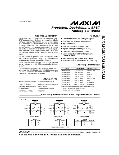
ELECTRICAL CHARACTERISTICS
(V+ = +5V ±10%, V- = -5V ±10%, VINH = 3.5V, VINL = 2.5V, TA = TMIN to TMAX, unless otherwise noted.)
PARAMETER ANALOG SWITCH Analog Signal Range
For equivalent devices specified for single-supply operation, see the MAX323/MAX324/MAX325 data sheet. For quad versions of these switches, see the MAX391/MAX392/MAX393 data sheet.
Plastic DIP (derate 9.09mW/°C above +70°C) .............727mW Narrow SO (derate 5.88mW/°C above +70°C) .............471mW
µMAX (derate 4.10mW/°C above +70°C) .....................330mW CERDIP (derate 8.00mW/°C above +70°C) ..................640mW Operating Temperature Ranges MAX32_C_ _ ........................................................0°C to +70°C MAX32_E_ _......................................................-40°C to +85°C MAX32_MJA ...................................................-55°C to +125°C Storage Temperature Range .............................-65°C to +150°C Lead Temperature (soldering, 10sec) .............................+300°C
MAX512使用手册

MAX 512 MOVING LIGHT CONTROLLER电脑灯控制台 - 用户手册(软件版本VER:3.8)Net.DO力度灯控设备有限公司NETDO LIGHTING CONTROL EQUIPMENT CO.,LTD目录一、综述 (4)1.1 功能特点 (4)1.2 规格参数 (4)二、安装 (5)2.1安全使用注意事项 (5)2.2 连接供电电源 (5)2.3 连接电脑灯和数码调光设备 (5)2.4 音频信号源 (5)三、操作使用 (6)3.1 面板图 (6)3.2 常用词汇介绍 (7)3.3 键盘部分 (7)3.4 推杆、数据轮部分 (9)3.5 后板接口说明 (10)四、设置电脑灯 (11)4.1了解您的电脑灯 (11)4.2 X/Y(PAN/TILT)通道解析 (11)4.3电脑灯的DMX512 地址码分配及X/Y设置 (11)4.3.1 固定分配电脑灯地址: (11)4.3.2动态分配电脑灯地址: (11)4.3.3设置的方法及步骤: (12)五、电脑灯的手动运行(手动场景) (13)5.1 CHANNEL通道推杆与数据轮 (13)5.2 电脑灯的手动运行 (13)5.3 取消电脑灯的手动运行 (13)六、场景编辑 (14)6.1 重要提示 (14)6.2 场景的编辑记录步骤 (14)6.3 场景的复制 (14)七、走灯程序编辑 (15)7.1 走灯程序的编辑步骤: (15)八、运行 (17)8.1 运行场景 (17)8.2 运行走灯程序 (17)8.2.1 查看各走灯程序的运行状态 (18)8.2.2 走灯的同步触发模式 (18)8.2.3 调节自动模式(Auto)下的SPEED% 及CROSS% 值 (18)九、图形轨迹(SHAPE) (19)9.1 图形轨迹发生器 (19)9.2 图形的调用与编辑 (19)9.3 图形的停止与运行 (21)9.4 清除电脑灯的图形调用 (21)9.5 查看图形的调用情况 (21)9.6 图形的使用技巧 (21)十、数据文件的加载与保存 (24)10.1 闪存卡的使用 (24)10.2 文件的保存(SA VE) (24)10.3 文件的加载(LOAD) (24)十一.数据的初始化 (25)十二.附表 (25)12.1 LCD显示内容解释: (25)1.1 功能特点MAX512电脑灯光控制台可同时控制30台最大32通道的电脑灯,其核心微电脑采用新的技术,使其获得了更强、更人性化的功能。
MAX312LESE中文资料

MAX312L/MAX313L/MAX314L
10Ω, Quad, SPST, +3V Logic-Compatible Analog Switches
ABSOLUTE MAXIMUM RATINGS
(Voltages Referenced to GND) V+ ...........................................................................-0.3V to +44V V- ............................................................................+0.3V to -44V V+ to V-...................................................................-0.3V to +44V VIN_ to V- ................................................................-0.3V to +44V All Other Pins (Note 1) ..........................(V- - 0.3V) to (V+ + 0.3V) Continuous Current (COM_, NO_, NC_) ........................±100mA Peak Current (COM_, NO_, NC_)
Turn-On Time
Turn-Off Time
Break-Before-Make Time Delay (MAX314L only, Note 7)
MAX3232EEAE中文资料

MAX3222EEPN -40°C to +85°C 18 Plastic DIP —
MAX3232ECAE 0°C to +70°C 16 SSOP
—
MAX3232ECWE 0°C to +70°C 16 Wide SO —
MAX3232ECPE 0°C to +70°C 16 Plastic DIP —
General Description
The MAX3222E/MAX3232E/MAX3237E/MAX3241E/ MAX3246E +3.0V-powered EIA/TIA-232 and V.28/V.24 communications interface devices feature low power consumption, high data-rate capabilities, and enhanced electrostatic-discharge (ESD) protection. The enhanced ESD structure protects all transmitter outputs and receiver inputs to ±15kV using IEC 1000-4-2 Air-Gap Discharge, ±8kV using IEC 1000-4-2 Contact Discharge (±9kV for MAX3246E), and ±15kV using the Human Body Model. The logic and receiver I/O pins of the MAX3237E are protected to the above standards, while the transmitter output pins are protected to ±15kV using the Human Body Model.
- 1、下载文档前请自行甄别文档内容的完整性,平台不提供额外的编辑、内容补充、找答案等附加服务。
- 2、"仅部分预览"的文档,不可在线预览部分如存在完整性等问题,可反馈申请退款(可完整预览的文档不适用该条件!)。
- 3、如文档侵犯您的权益,请联系客服反馈,我们会尽快为您处理(人工客服工作时间:9:00-18:30)。
For pricing, delivery, and ordering information, please contact Maxim/Dallas Direct! at 1-888-629-4642, or visit Maxim’s website at .
Applications
Industrial Process Control Automatic Test Equipment Digital Offset and Gain Adjustment Motion Control Microprocessor-Controlled Systems
Note: All devices are specified over the -40°C to +85°C operating temperature range.
Features
MAX5122/MAX5123
Ordering Information
PART MAX5122AEEE MAX5122BEEE MAX5123AEEE MAX5123BEEE PINPACKAGE 16 QSOP 16 QSOP 16 QSOP 16 QSOP INL (LSB) ±0.5 ±1 ±1 ±2 PKG CODE E16-5 E16-5 E16-5 E16-5
元器件交易网
19-1446; Rev 2; 5/06
+5V/+3V, 12-Bit, Serial, Force/Sense DACs with 10ppm/°C Internal Reference
General Description
The MAX5122/MAX5123 low-power, 12-bit, voltage-output, digital-to-analog converters (DACs) feature an internal precision bandgap reference and output amplifier. The MAX5122 operates on a single +5V supply with an internal +2.5V reference, and offers a configurable output amplifier. If necessary, the user can override the on-chip, <10ppm/°C voltage reference with an external reference. The MAX5123 has the same features as the MAX5122 but operates from a single +3V supply and has an internal +1.25V precision reference. The user-accessible inverting input and output of the amplifier allows specific gain configurations, remote sensing, and high output drive capability for a wide range of force/sense applications. Both devices draw only 500µA of supply current, which reduces to 3µA in power-down mode. In addition, their power-up reset feature allows for a user-selectable initial output state of either 0V or midscale and reduces output glitches during power-up. The serial interface is compatible with SPI™, QSPI™, and MICROWIRE™, which makes the MAX5122/MAX5123 suitable for cascading multiple devices. Each DAC has a double-buffered input organized as an input register followed by a DAC register. A 16-bit shift register loads data into the input register. The DAC register may be updated independently or simultaneously with the input register. Both devices are available in a 16-pin QSOP package and are specified for the extended-industrial (-40°C to +85°C) operating temperature range. For pin-compatible 14-bit upgrades, see the MAX5171/MAX5173 data sheet; for the pin-compatible 13-bit version, see the MAX5132/ MAX5133 data sheet. ♦ Single-Supply Operation +5V (MAX5122) +3V (MAX5123) ♦ Built-In 10ppm/°C max Precision Bandgap Reference +2.5V (MAX5122) +1.25V (MAX5123) ♦ SPI/QSPI/MICROWIRE-Compatible, 3-Wire Serial Interface ♦ Pin-Programmable Shutdown Mode and PowerUp Reset (0 or Midscale Output Voltage) ♦ Buffered Output Capable of Driving 5kΩ 100pF or 4–20mA Loads ♦ Space-Saving 16-Pin QSOP Package ♦ Pin-Compatible 13-Bit Upgrades Available (MAX5132/MAX5133) ♦ Pin-Compatible 14-Bit Upgrades Available (MAX5171/MAX5173)
Pin Configuration
TOP VIEW
FB 1 OUT 2 RSTVAL 3 PDL 4 CLR 5 CS 6 DIN 7 SCLK 8 16 VDD 15 REFADJ 14 REF
MAX5122 MAX5123
13 AGND 12 PD 11 UPO 10 DOUT 9 DGND
SPI and QSPI are trademarks of Motorola, Inc. MICROWIRE is a trademark of National Semiconductor Corp.
Stresses beyond those listed under “Absolute Maximum Ratings” may cause permanent damage to the device. These are stress ratings only, and functional operation of the device at these or any other conditions beyond those indicated in the operational sections of the specifications is not implied. Exposure to absolute maximum rating conditions for extended periods may affect device reliability.
ELECTRICAL CHARACTERISTICS—MAX5122 (+5V)
(VDD = +5V ±10%, AGND = DGND, 33nF capacitor at REFADJ, internal reference, RL = 5kΩ, CL = 100pF, output amplifier configured in unity-gain, TA = TMIN to TMAX, unless otherwise noted. Typical values are at TA = +25°C.) PARAMETER STATIC PERFORMANCE Resolution Integral Nonlinearity (Note 1) Differential Nonlinearity Offset Error (Note 2) Gain Error Full-Scale Temperature Coefficient (Note 3) Power-Supply Rejection Ratio REFERENCE Output Voltage Output Voltage Temperature Coefficient Reference External Load Regulation Reference Short-Circuit Current REFADJ Current DIGITAL INPUT Input High Voltage Input Low Voltage Input Hysteresis Input Leakage Current Input Capacitance DIGITAL OUTPUTS Output High Voltage Output Low Voltage VOH VOL ISOURCE = 2mA ISINK = 2mA VDD - 0.5 0.13 0.4 V V VIH VIL VHYS IIN CIN VIN = 0 or VDD -1 200 0.001 8 1 3 0.8 V V mV µA pF REFADJ = VDD VREF TCVREF VOUT/IOUT TA = +25°C MAX5122A MAX5122B 0 ≤ IOUT ≤ 100µA (sourcing) 2.475 2.5 3 10 0.1 4 3.3 7 1 2.525 V ppm/°C µV/µA mA µA N INL DNL VOS GE TCVFS PSRR MAX5122A MAX5123B 4.5V ≤ VDD ≤ 5.5V MAX5122A MAX5123B 12 -0.5 -1 -1 -10 -3 -0.2 3 10 20 0.5 1 1 10 3 10 30 250 Bits LSB LSB mV mV ppm/°C µV/V SYMBOL CONDITIONS MIN TYP MAX UNITS