P6SMB6中文资料
硕凯P6SMB600A贴片瞬态抑制器件

硕凯P6SMB600A贴片瞬态抑制器件硕凯电子(Sylvia)一、瞬态抑制器说明瞬态二极管(Transient Voltage Suppressor)简称TVS管,TVS管的电气特性是由P-N结面积、掺杂浓度及晶片阻质决定的。
其耐突波电流的能力与其P-N结面积成正比。
TVS广泛应用于半导体及敏感器件的保护,通常用于二级电源和信号电路的保护,以及防静电等。
其特点为反应速度快(为ps级),体积小,脉冲功率较大,箝位电压低等。
其10/1000μs波脉冲功率从400W~30KW,脉冲峰值电流从0.52A~544A;击穿电压有从6.8V~550V的系列值,便于各种不同电压的电路使用。
二、脉冲降额曲线三、瞬态抑制器产品图四、产品特性1、为表面安装应用优化电路板空间2、低泄漏3、单向和双向单元4、玻璃钝化结5、低电感6、优良的钳位能力7、600W的峰值功率能力在10×1000μ波形重复率(占空比):0.01%8、快速响应时间:从0伏特到最小击穿电压通常小于1.0ps9、典型的,在电压高于12V时,反向漏电流小于5μA10、高温焊接:终端260°C/40秒11、典型的最大温度系数△Vbr=0.1%x Vbr@25°C x△T12、塑料包装有保险商实验室可燃性94V-013、无铅镀雾锡14、无卤化,符合RoHS15、典型失效模式是在指定的电压或电流下出现16、晶须测试是基于JEDEC JESD201A每个表4a及4c进行的17、IEC-61000-4-2ESD15kV(空气),8kV(接触)18、数据线的ESD保护符合IEC61000-4-2(IEC801-2)19、数据线的EFT保护符合IEC61000-4-4(IEC801-4)五、编带和卷盘说明六、环境规定七、最大额定值Notes:1.Non-repetitive current pulse,per Fig.3and derated above TA=25°C per Fig.2.2.Mounted on5.0mm x5.0mm(0.03mm thick)Copper Pads to each terminal.3.8.3ms single half sine-wave,or equivalent square wave,Duty cycle=4pulses per minutes maximum.4.VF<3.5V for VBR<200V and VF<6.5V for VBR>201V.八、功能线路图九、英文描述The P6SMB series is designed specifically to protect sensitive electronic equipment from voltage transients induced by lightning and other transient voltage events.十、I-V曲线特性十一、产品应用TVS器件非常适合保护I/O接口,Vcc总线和其他应用于电信、计算机、工业和消费电子应用的易损电路。
P6SMB51CAT3资料

P6SMB11CAT3 Series600 Watt Peak Power Zener Transient Voltage Suppressors Bidirectional*The SMB series is designed to protect voltage sensitive components from high voltage, high energy transients. They have excellent clamping capability, high surge capability, low zener impedance and fast response time. The SMB series is supplied in ON Semiconductor’s exclusive, cost-effective, highly reliable Surmetic t package and is ideally suited for use in communication systems, automotive, numerical controls, process controls, medical equipment, business machines, power supplies and many other industrial/consumer applications.Features•Working Peak Reverse V oltage Range − 9.4 to 77.8 V •Standard Zener Breakdown V oltage Range − 11 to 91 V •Peak Power − 600 W @ 1 ms•ESD Rating of Class 3 (>16 KV) per Human Body Model •Maximum Clamp V oltage @ Peak Pulse Current•Low Leakage < 5 m A Above 10 V•UL 497B for Isolated Loop Circuit Protection •Response Time is Typically < 1 ns•Pb−Free Packages are AvailableMechanical Characteristics:CASE:V oid-Free, Transfer-Molded, Thermosetting Plastic FINISH:All External Surfaces are Corrosion Resistant and Leads are Readily SolderableMAXIMUM CASE TEMPERATURE FOR SOLDERING PURPOSES: 260°C for 10 SecondsLEADS:Modified L−Bend Providing More Contact Area to Bond Pads POLARITY:Polarity Band Will Not be IndicatedMOUNTING POSITION:AnyMAXIMUM RATINGSRating Symbol Value Unit Peak Power Dissipation (Note 1) @ T L = 25°C,Pulse Width = 1 msP PK600WDC Power Dissipation @ T L = 75°C Measured Zero Lead Length (Note 2) Derate Above 75°CThermal Resistance, Junction−to−LeadP DR q JL3.04025WmW/°C°C/WDC Power Dissipation (Note 3) @ T A = 25°C Derate Above 25°CThermal Resistance, Junction−to−AmbientP DR q JA0.554.4226WmW/°C°C/WOperating and Storage Temperature Range T J, Tstg−65 to+150°CStresses exceeding Maximum Ratings may damage the device. Maximum Ratings are stress ratings only. Functional operation above the Recommended Operating Conditions is not implied. Extended exposure to stresses above the Recommended Operating Conditions may affect device reliability.1.10 X 1000 m s, non−repetitive2.1″ square copper pad, FR−4 board3.FR−4 board, using ON Semiconductor minimum recommended footprint, asshown in 403A case outline dimensions spec.*Please see P6SMB6.8AT3 to P6SMB200AT3 for Unidirectional devices.Devices listed in bold, italic are ON Semiconductor Preferred devices. Preferred devices are recommended choices for future use and best overall value.Device Package Shipping†ORDERING INFORMATIONP6SMBxxCAT3SMB2500/T ape & ReelP6SMBxxCAT3G SMB(Pb−Free)2500/T ape & Reel†For information on tape and reel specifications, including part orientation and tape sizes, please refer to our T ape and Reel Packaging Specifications Brochure, BRD8011/D.The “T3” suffix refers to a 13 inch reel.ELECTRICAL CHARACTERISTICS(T A = 25°C unless otherwise noted)Symbol ParameterI PP Maximum Reverse Peak Pulse CurrentV C Clamping Voltage @ I PPV RWM Working Peak Reverse VoltageI R Maximum Reverse Leakage Current @ V RWMV BR Breakdown Voltage @ I TI T Test CurrentQ V BR Maximum Temperature Coefficient of V BRELECTRICAL CHARACTERISTICS (Devices listed in bold, italic are ON Semiconductor Preferred devices.)Device*DeviceMarkingV RWM(Note 4)I R@V RWMBreakdown Voltage V C @ I PP(Note 6)Q V BRC typ(Note 7)V BR Volts (Note 5)@ I T V C I PPVolts m A Min Nom Max mA Volts Amps%/°C pFP6SMB11CAT3, G P6SMB12CAT3, G P6SMB13CAT3, G 11C12C13C9.410.211.155510.511.412.411.051213.0511.612.613.711115.616.718.23836330.0750.0780.081865800740P6SMB15CAT3, G P6SMB16CAT3, G P6SMB18CAT3, G P6SMB20CAT3, G 15C16C18C20C12.813.615.317.1555514.315.217.11915.0516182015.816.818.921111121.222.525.227.7282724220.0840.0860.0880.09645610545490P6SMB22CAT3, G P6SMB24CAT3, G P6SMB27CAT3, G P6SMB30CAT3, G 22C24C27C30C18.820.523.125.6555520.922.825.728.5222427.053023.125.228.431.5111130.633.237.541.420181614.40.090.0940.0960.097450415370335P6SMB33CAT3, G P6SMB36CAT3, G P6SMB39CAT3, G P6SMB43CAT3, G 33C36C39C43C28.230.833.336.8555531.434.237.140.933.053639.0543.0534.737.84145.2111145.749.953.959.313.21211.210.10.0980.0990.10.101305280260240P6SMB47CAT3, G P6SMB51CAT3, G P6SMB56CAT3, G P6SMB62CAT3, G 47C51C56C62C40.243.647.853555544.748.553.258.947.0551.05566249.453.658.865.1111164.870.177859.38.67.87.10.1010.1020.1030.104220205185170P6SMB68CAT3, G P6SMB75CAT3, G P6SMB82CAT3, G P6SMB91CAT3, G 68C75C82C91C58.164.170.177.8555564.671.377.986.56875.05829171.478.886.195.51111921031131256.55.85.34.80.1040.1050.1050.1061551401301204. A transient suppressor is normally selected according to the working peak reverse voltage (V RWM), which should be equal to or greater thanthe DC or continuous peak operating voltage level.5.V BR measured at pulse test current I T at an ambient temperature of 25°C.6.Surge current waveform per Figure 2 and derate per Figure 3 of the General Data − 600 Watt at the beginning of this group.7.Bias Voltage = 0 V, F = 1 MHz, T J = 25°C*The “G’’ suffix indicates Pb−Free package available. Please refer back to Ordering Information on front page.P , P E A K P O W E R (k W )P 1101000.1t, TIME (ms)Figure 2. Pulse WaveformTYPICAL PROTECTION CIRCUITFigure 3. Pulse Derating CurveP E A K P U L S E D E R A T I N G I N % O F P E A K P O W E R O R C U R R E N T @ T A = 25C°T A , AMBIENT TEMPERATURE (°C)Figure 4. Typical Junction Capacitance vs. BiasVoltageBIAS VOLTAGE (VOLTS)110100C , C A P A C I T A N C E (p F )APPLICATION NOTESRESPONSE TIMEIn most applications, the transient suppressor device is placed in parallel with the equipment or component to be protected. In this situation, there is a time delay associated with the capacitance of the device and an overshoot condition associated with the inductance of the device and the inductance of the connection method. The capacitive effect is of minor importance in the parallel protection scheme because it only produces a time delay in the transition from the operating voltage to the clamp voltage as shown in Figure 4.The inductive effects in the device are due to actual turn-on time (time required for the device to go from zero current to full current) and lead inductance. This inductive effect produces an overshoot in the voltage across the equipment or component being protected as shown in Figure 5. Minimizing this overshoot is very important in the application, since the main purpose for adding a transient suppressor is to clamp voltage spikes. The SMB series have a very good response time, typically < 1 ns and negligible inductance. However, external inductive effects could produce unacceptable overshoot. Proper circuit layout, minimum lead lengths and placing the suppressor device as close as possible to the equipment or components to be protected will minimize this overshoot. Some input impedance represented by Z in is essential to prevent overstress of the protection device. This impedance should be as high as possible, without restricting the circuit operation.DUTY CYCLE DERATINGThe data of Figure 1 applies for non-repetitive conditions and at a lead temperature of 25°C. If the duty cycle increases, the peak power must be reduced as indicated by the curves of Figure 6. A verage power must be derated as the lead or ambient temperature rises above 25°C. The average power derating curve normally given on data sheets may be normalized and used for this purpose.At first glance the derating curves of Figure 6 appear to be in error as the 10 ms pulse has a higher derating factor than the 10 m s pulse. However, when the derating factor for a given pulse of Figure 6 is multiplied by the peak power value of Figure 1 for the same pulse, the results follow the expected trend.VFigure 5. Figure 6.Figure 7. Typical Derating Factor for Duty CycleD E R A T I N GF A C T O R10.70.50.30.050.10.010.020.030.07D, DUTY CYCLE (%)UL RECOGNITIONThe entire series has Underwriters Laboratory Recognition for the classification of protectors (QVGV2)under the UL standard for safety 497B and File #116110.Many competitors only have one or two devices recognized or have recognition in a non-protective category. Some competitors have no recognition at all. With the UL497B recognition, our parts successfully passed several testsincluding Strike V oltage Breakdown test, Endurance Conditioning, Temperature test, Dielectric V oltage-Withstand test, Discharge test and several more.Whereas, some competitors have only passed a flammability test for the package material, we have been recognized for much more to be included in their Protector category.PACKAGE DIMENSIONSSMBDO−214AACASE 403A−03ISSUE F*For additional information on our Pb−Free strategy and solderingdetails, please download the ON Semiconductor Soldering andMounting Techniques Reference Manual, SOLDERRM/D.SURMETIC is a trademark of Semiconductor Components Industries, LLC.ON Semiconductor and are registered trademarks of Semiconductor Components Industries, LLC (SCILLC). SCILLC reserves the right to make changes without further notice to any products herein. SCILLC makes no warranty, representation or guarantee regarding the suitability of its products for any particular purpose, nor does SCILLC assume any liability arising out of the application or use of any product or circuit, and specifically disclaims any and all liability, including without limitation special, consequential or incidental damages.“Typical” parameters which may be provided in SCILLC data sheets and/or specifications can and do vary in different applications and actual performance may vary over time. All operating parameters, including “Typicals” must be validated for each customer application by customer’s technical experts. SCILLC does not convey any license under its patent rights nor the rights of others. SCILLC products are not designed, intended, or authorized for use as components in systems intended for surgical implant into the body, or other applications intended to support or sustain life, or for any other application in which the failure of the SCILLC product could create a situation where personal injury or death may occur. Should Buyer purchase or use SCILLC products for any such unintended or unauthorized application, Buyer shall indemnify and hold SCILLC and its officers, employees, subsidiaries, affiliates, and distributors harmless against all claims, costs, damages, and expenses, and reasonable attorney fees arising out of, directly or indirectly, any claim of personal injury or death associated with such unintended or unauthorized use, even if such claim alleges that SCILLC was negligent regarding the design or manufacture of the part. SCILLC is an Equal Opportunity/Affirmative Action Employer. This literature is subject to all applicable copyright laws and is not for resale in any manner.PUBLICATION ORDERING INFORMATION。
P6SMBJ85A中文资料
V C @ IPP V A
PAC K AGE
600W Transient Voltage S uppressor
P 6S MB J5.0(C ) P 6S MB J5.0(C )A P 6S MB J6.0(C ) P 6S MB J6.0(C )A P 6S MB J6.5(C ) P 6S MB J6.5(C )A P 6S MB J7.0(C ) P 6S MB J7.0(C )A P 6S MB J7.5(C ) P 6S MB J7.5(C )A P 6S MB J8.0(C ) P 6S MB J8.0(C )A P 6S MB J8.5(C ) P 6S MB J8.5(C )A P 6S MB J9.0(C ) P 6S MB J9.0(C )A P 6S MB J10(C ) P 6S MB J10(C )A P 6S MB J11(C ) P 6S MB J11(C )A P 6S MB J12(C ) P 6S MB J12(C )A P 6S MB J13(C ) P 6S MB J13(C )A P 6S MB J14(C ) P 6S MB J14(C )A P 6S MB J15(C ) P 6S MB J15(C )A P 6S MB J16(C ) P 6S MB J16(C )A P 6S MB J17(C ) P 6S MB J17(C )A P 6S MB J18(C ) P 6S MB J18(C )A P 6S MB J20(C ) P 6S MB J20(C )A P 6S MB J22(C ) P 6S MB J22(C )A P 6S MB J24(C ) P 6S MB J24(C )A P 6S MB J26(C ) P 6S MB J26(C )A P 6S MB J28(C ) P 6S MB J28(C )A P 6S MB J30(C ) P 6S MB J30(C )A P 6S MB J33(C ) P 6S MB J33(C )A P 6S MB J36(C ) P 6S MB J36(C )A P 6S MB J40(C ) P 6S MB J40(C )A KD KE KF KG KH KK KL KM KN KP KQ KR KS KT KU KV KW KX KY KZ LD LE LF LG LH LK LL LM LN LP LQ LR LS LT LU LV LW LX LZ LY MD ME MF MG MH MK ML MM MN MP MQ MR AD AE AF AG AH AK AL AM AN AP AQ AR AS AT AU AV AW AX AY AZ BD BE BF BG BH BK BL BM BN BP BQ BR BS BT BU BV BW BX BZ BY CD CE CF CG CH CK CL CM CN CP CQ CR 5.0 5.0 6.0 6.0 6.5 6.5 7.0 7.0 7.5 7.5 8.0 8.0 8.5 8.5 9.0 9.0 10 10 11 11 12 12 13 13 14 14 15 15 16 16 17 17 18 18 20 20 22 22 24 24 26 26 28 28 30 30 33 33 36 36 40 40 6.40 6.40 6.67 6.67 7.22 7.22 7.78 7.78 8.33 8.33 8.89 8.89 9.44 9.44 10.0 10.0 11.1 11.1 12.2 12.2 13.3 13.3 14.4 14.4 15.6 15.6 16.7 16.7 17.8 17.8 18.9 18.9 20.0 20.0 22.2 22.2 24.4 24.4 26.7 26.7 28.9 28.9 31.1 31.1 33.3 33.3 36.7 36.7 40.0 40.0 44.4 44.4 7.55 7.25 8.45 7.67 9.14 8.30 9.86 8.95 10.67 9.58 11.30 10.23 11.92 10.82 12.6 11.5 14.1 12.8 15.4 14.0 16.9 15.3 18.2 16.5 19.8 17.9 21.1 19.2 22.6 20.5 23.9 21.7 25.3 23.3 28.1 25.5 30.9 28.0 33.8 30.7 36.6 33.2 39.4 35.8 42.2 38.3 46.5 42.2 50.7 46.0 56.3 51.1 10 10 10 10 10 10 10 10 1.0 1.0 1.0 1.0 1.0 1.0 1.0 1.0 1.0 1.0 1.0 1.0 1.0 1.0 1.0 1.0 1.0 1.0 1.0 1.0 1.0 1.0 1.0 1.0 1.0 1.0 1.0 1.0 1.0 1.0 1.0 1.0 1.0 1.0 1.0 1.0 1.0 1.0 1.0 1.0 1.0 1.0 1.0 1.0 800 800 800 800 500 500 200 200 100 100 50 50 10 10 5 5 5 5 5 5 5 5 5 5 5 5 5 5 5 5 5 5 5 5 5 5 5 5 5 5 5 5 5 5 5 5 5 5 5 5 5 5 1600 1600 1600 1600 1000 1000 400 400 200 200 100 100 20 20 10 10 5 5 5 5 5 5 5 5 5 5 5 5 5 5 5 5 5 5 5 5 5 5 5 5 5 5 5 5 5 5 5 5 5 5 5 5 9.6 9.2 11.4 10.3 12.3 11.2 13.3 12.0 14.3 12.9 15.0 13.6 15.9 14.4 16.9 15.4 18.8 17.0 20.1 18.2 22.0 19.9 23.8 21.5 25.8 23.2 26.9 24.4 28.8 26.0 30.5 27.6 32.2 29.2 35.8 32.4 39.4 35.5 43.0 38.9 46.6 42.1 50.0 45.4 53.5 48.4 59.0 53.3 64.3 58.1 71.4 64.5 62.5 65.2 52.6 58.3 48.7 53.6 45.1 50.0 42.0 46.5 40.0 44.1 37.7 41.7 35.5 39.0 31.9 35.3 29.9 33.0 27.3 30.2 25.2 27.9 23.3 25.8 22.3 24.0 20.8 23.1 19.7 21.7 18.6 20.5 16.7 18.5 15.2 16.9 14.0 15.4 12.4 14.2 12.0 13.2 11.2 12.4 10.2 11.3 9.3 10.3 8.4 9.3 S MB /D O-214A A S MB /D O-214A A S MB /D O-214A A S MB /D O-214A A S MB /D O-214A A S MB /D O-214A A S MB /D O-214A A S MB /D O-214A A S MB /D O-214A A S MB /D O-214A A S MB /D O-214A A S MB /D O-214A A S MB /D O-214A A S MB /D O-214A A S MB /D O-214A A S MB /D O-214A A S MB /D O-214A A S MB /D O-214A A S MB /D O-214A A S MB /D O-214A A S MB /D O-214A A S MB /D O-214A A S MB /D O-214A A S MB /D O-214A A S MB /D O-214A A S MB /D O-214A A S MB /D O-214A A S MB /D O-214A A S MB /D O-214A A S MB /D O-214A A S MB /D O-214A A S MB /D O-214A A S MB /D O-214A A S MB /D O-214A A S MB /D O-214A A S MB /D O-214A A S MB /D O-214A A S MB /D O-214A A S MB /D O-214A A S MB /D O-214A A S MB /D O-214A A S MB /D O-214A A S MB /D O-214A A S MB /D O-214A A S MB /D O-214A A S MB /D O-214A A S MB /D O-214A A S MB /D O-214A A S MB /D O-214A A S MB /D O-214A A S MB /D O-214A A S MB /D O-214A A
特斯拉P6产品规格说明书
PB-08482-001_v02 | August 2017 Product BriefDOCUMENT CHANGE HISTORYPB-08482-001_v02Version Date Authors Description of Change01 March 24, 2017 VK, DV Initial release02 August 31, 2017 VK, DV Removed NVIDIA Confidential informationTABLE OF CONTENTS Overview (1)Specifications (3)Product Specification (3)Design Discussion (5)Form Factor (5)MXM PCB Mounting Holes (6)Compute Mode (8)Support Information (9)Certificates and Agencies (9)Certifications (9)Agencies (9)LIST OF FIGURES Figure 1. Tesla P6 Board (2)Figure 2. Tesla P6 Board Outline (5)Figure 3. Mounting Holes (6)LIST OF TABLES Table 1. Product Specifications (3)Table 2. Memory Specifications (4)Table 3. Software Feature Specifications (4)Table 4. Thermal Specifications (4)Table 5. Tesla P6 Board Outline Specifications (6)Table 6. Mounting Holes Specifications (7)Table 7. Compute Mode Settings (8)The NVIDIA® Tesla® P6 is an MXM 3.1 Type B card with a single NVIDIA® Pascal™GP104 graphics processing unit (GPU). It has 16 GB GDDR5 video memory and a 90 Watt maximum power limit.This board is intended for accelerated graphics in virtual remote workstation and virtual desktop environments, as well as for single precision GPU compute tasks. Tesla P6 is specifically optimized for space constrained systems like blade servers.NVIDIA does not ship this board with a cooling solution attached, however NVIDIA does provide thermal specifications for OEMs to design their custom heat sinks.A main feature of the Tesla P6 board is the support of NVIDIA® GRID™ software which includes NVIDIA® GRID™ vGPU™. This technology enables the virtualization of physical GPUs into full-featured virtual GPUs providing maximum performance and scalability.For performance optimization, this board utilizes NVIDIA GPU BOOST™. By adjusting the GPU clock dynamically, maximum performance is achieved within the power cap limit (90 W).Tesla P6 supports H.264 and H.265 hardware encoding, which is particularly important for reducing round-trip latency and image quality for virtual desktops and applications.OverviewFigure 1. Tesla P6 BoardPRODUCT SPECIFICATIONTable 1 provides the product specifications for the Tesla P6 board. Table 1. Product SpecificationsSpecification DescriptionBoard SKU PG418 SKU 200Total board power 90 W (70 W optional)GPU SKU GP104-995IDs DEVID: 0x1BB4SSID: 0x11C6Form Factor MXM 3.1 Type BNVIDIA® CUDA® cores 2048GPU clocks Base 1012 MHz (TGP: 90 W) Boost 1506 MHz (TGP: 90 W)PCI Express interface P0: Gen3 16 lanes, 16.0 GbpsP8: Gen1 16 lanes, 2.5 GbpsSpecificationsTable 2 provides the memory specifications for the Tesla P6 graphics board.Table 2. Memory SpecificationsSpecification DescriptionMemory clock 3003 MHzMemory size 16 GBMemory I/O 256-bitMemory configuration 16 pcs 256M × 16 GDDR5sMemory bandwidth 192.2 GB/sTable 3 provides the software feature specifications.Table 3. Software Feature SpecificationsSpecification DescriptionEEPROM size 4 Mb Serial ROMPCI class code PCI base class: 0x03PCI sub-class: 0x02ECC support Supported (enabled by default)SMBPBI (SMBus Post Box Interface) SupportedTable 4 provides the thermal specifications for the Tesla P6 graphics board.Table 4. Thermal SpecificationsAction T j (°C)GPU shutdown temperature 94GPU slowdown temperature 91GPU maximum operating temperature 89GPU hardware slowdown amount 50%FORM FACTORTesla P6 follows the MXM 3.1 Type B mechanical specifications. For more details on the mechanical specifications, refer to the latest version of the MXM Electromechanical Specification.Figure 2. Tesla P6 Board OutlineTable 5. Tesla P6 Board Outline SpecificationsSymbolmm inchesMinimum Nominal Maximum Minimum Nominal MaximumA1 82.00 3.228A2 70.00 2.756A3 105.00 4.134A4 3.37 3.50 3.63 0.133 0.138 0.143A5 78.37 78.50 78.63 3.085 3.091 3.096A6 3.87 4.00 4.13 0.152 0.157 0.163A7 65.87 66.00 66.13 2.593 2.598 2.604A8 38.87 39.00 39.13 1.530 1.535 1.541MXM PCB MOUNTING HOLESThe module has six holes. Two are used to secure the board to the system and the other four to fasten the thermal solution to the module.Figure 3. Mounting HolesTable 6. Mounting Holes SpecificationsSymbolmm inchesMinimum Nominal Maximum Minimum Nominal MaximumB1 75.00 2.953B2 8.25 0.325B3 54.25 2.136B4 5.50 0.217B5 51.50 2.028B6 3.07 3.20 3.33 0.121 0.126 0.131 B7 3.07 3.20 3.33 0.121 0.126 0.131In contrast to Tesla M6, Tesla P6 is offered only in compute mode. Starting with Pascal-generation boards, switching between graphics and compute mode is no longerrequired. NVIDIA GRID software automatically handles most setting adjustments previously requiring the switch to graphics mode. Nevertheless, ECC must be disabledbefore running NVIDIA GRID software.Table 7 provides details of the compute mode settings.Table 7. Compute Mode SettingsSetting Value NotesClass code 3D Controller This class code indicates to operatingsystems (OS) that the GPU is not intendedfor use as a primary display device. Memory BAR 16 gigabytes Tesla GPUs expose a large memory baseaddress register (BAR) for direct access tothe frame buffer from the CPU, and otherPCI Express devices.I/O base BAR Disabled The GPU need not consume any legacy I/Oresources when used as a non-displaydevice.ECC protection Enabled Error Correcting Code (ECC) is enabled onthe GPU frame buffer to protect againstsingle- and multi-bit memory errors. ECCcan be turned off.CERTIFICATES AND AGENCIESCertifications④Windows Hardware Quality Lab (WHQL):●Certified Windows 7, Windows 8.1, and Windows 10●Certified Windows Server 2008 R2, Windows Server 2012 R2, and Windows Server2016④EU Reduction of Hazardous Substances (EU RoHS)④Joint Industry guide (J-STD) / Registration, Evaluation, Authorization, and Restriction of Chemical Substance (EU) – (JIG / REACH)④Halogen Free (HF)④EU Waste Electrical and Electronic Equipment (WEEE)Agencies④Australian Communications Authority and Radio Spectrum Management Group of New Zealand (C-Tick)④Bureau of Standards, Metrology, and Inspection (BSMI)④Conformité Européenne (CE)④Federal Communications Commission (FCC)④Industry Canada - Interference-Causing Equipment Standard (ICES)④Underwriters Laboratories (cUL, UL)④Voluntary Control Council for Interference (VCCI)NoticeThe information provided in this specification is believed to be accurate and reliable as of the date provided. However, NVIDIA Corporation (“NVIDIA”) does not give any representations or warranties, expressed or implied, as to the accuracy or completeness of such information. NVIDIA shall have no liability for the consequences or use of such information or for any infringement of patents or other rights of third parties that may result from its use. This publication supersedes and replaces all other specifications for the product that may have been previously supplied.NVIDIA reserves the right to make corrections, modifications, enhancements, improvements, and other changes to this specification, at any time and/or to discontinue any product or service without notice. Customer should obtain the latest relevant specification before placing orders and should verify that such information is current and complete.NVIDIA products are sold subject to the NVIDIA standard terms and conditions of sale supplied at the time of order acknowledgement, unless otherwise agreed in an individual sales agreement signed by authorized representatives of NVIDIA and customer. NVIDIA hereby expressly objects to applying any customer general terms and conditions with regard to the purchase of the NVIDIA product referenced in this specification.NVIDIA products are not designed, authorized or warranted to be suitable for use in medical, military, aircraft, space or life support equipment, nor in applications where failure or malfunction of the NVIDIA product can reasonably be expected to result in personal injury, death or property or environmental damage. NVIDIA accepts no liability for inclusion and/or use of NVIDIA products in such equipment or applications and therefore such inclusion and/or use is at customer’s own risk.NVIDIA makes no representation or warranty that products based on these specifications will be suitable for any specified use without further testing or modification. Testing of all parameters of each product is not necessarily performed by NVIDIA. It is customer’s sole responsibility to ensure the product is suitable and fit for the application planned by customer and to do the necessary testing for the application in order to avoid a default of the application or the product. Weaknesses in customer’s product designs may affect the quality and reliability of the NVIDIA product and may result in additional or different conditions and/or requirements beyond those contained in this specification. NVIDIA does not accept any liability related to any default, damage, costs or problem which may be based on or attributable to: (i) the use of the NVIDIA product in any manner that is contrary to this specification, or (ii) customer product designs.No license, either expressed or implied, is granted under any NVIDIA patent right, copyright, or other NVIDIA intellectual property right under this specification. Information published by NVIDIA regarding third-party products or services does not constitute a license from NVIDIA to use such products or services or a warranty or endorsement thereof. Use of such information may require a license from a third party under the patents or other intellectual property rights of the third party, or a license from NVIDIA under the patents or other intellectual property rights of NVIDIA. Reproduction of information in this specification is permissible only if reproduction is approved by NVIDIA in writing, is reproduced without alteration, and is accompanied by all associated conditions, limitations, and notices.ALL NVIDIA DESIGN SPECIFICATIONS, REFERENCE BOARDS, FILES, DRAWINGS, DIAGNOSTICS, LISTS, AND OTHER DOCUMENTS (TOGETHER AND SEPARATELY, “MATERIALS”) ARE BEING PROVIDED “AS IS.” NVIDIA MAKES NO WARRANTIES, EXPRESSED, IMPLIED, STATUTORY, OR OTHERWISE WITH RESPECT TO THE MATERIALS, AND EXPRESSLY DISCLAIMS ALL IMPLIED WARRANTIES OF NONINFRINGEMENT, MERCHANTABILITY, AND FITNESS FOR A PARTICULAR PURPOSE. Notwithstanding any damages that customer might incur for any reason whatsoever, NVIDIA’s aggregate and cumulative liability towards customer for the products described herein shall be limited in accordance with the NVIDIA terms and conditions of sale for the product.TrademarksNVIDIA, the NVIDIA logo, BOOST, CUDA, GRID, Pascal, and Tesla are trademarks and/or registered trademarks of NVIDIA Corporation in the U.S. and other countries. Other company and product names may be trademarks of the respective companies with which they are associated.Copyright© 2017 NVIDIA Corporation. All rights reserved.。
P6SMB-Series规格书

MECHANICAL DATACase: SMB (DO-214AA)Molding compound meets UL 94 V-0 flammability rating Base P/N-E3 - RoHS-compliant, commercial gradeBase P/N-M3 - halogen-free, RoHS-compliant, commercial gradeBase P/NHE3_X - RoHS-compliant and AEC-Q101 qualified Base P/NHM3_X - halogen-free, RoHS-compliant, and AEC-Q101 qualified(“_X” denotes revision code e.g. A, B, ..... and only available for 250 V to 540 V type)Terminals: matte tin plated leads, solderable per J-STD-002 and JESD 22-B102E3, M3, HE3, and HM3 suffix meets JESD 201 class 2 whisker testPolarity: for uni-directional types the band denotes cathode end, no marking on bi-directional typesNotes(1) Non-repetitive current pulse, per fig. 3 and derated above T A= 25 °C per fig. 2 (2) Mounted on 0.2" x 0.2" (5.0 mm x 5.0 mm) copper pads to each terminalFEATURES• Low profile package• Ideal for automated placement • Glass passivated chip junction• Available in uni-directional and bi-directional • 600 W peak pulse power capability with a 10/1000 μs waveform, repetitive rate (duty cycle): 0.01 %• Excellent clamping capability • Very fast response time• Low incremental surge resistance• Meets MSL level 1, per J-STD-020, LF maximum peak of 260 °C• AEC-Q101 qualified available- Automotive ordering code: base P/NHE3 or P/NHM3(1) Pulse test: t p 50 ms(2) Surge current waveform per fig. 3 and derate per fig. 2(3) For bi-directional types with V WM of 10 V and less, the I D limit is doubled(4) All terms and symbols are consistent with ANSI/IEEE CA62.35(5) V F = 3.5 V at I F = 50 A (uni-directional only)RATINGS AND CHARACTERISTICS CURVES (T A = 25 °C unless otherwise noted)1001011007550250.10.1 µs 1.0 µs 10 µs 100 µs 1.0 ms 10 ms0 25 50 75 100125 150 175 200t d - Pulse Width (s) TJ - Initial Temperature (°C) Fig. 1 - Peak Pulse Power Rating Curve Fig. 2 - Pulse Power or Current vs. Initial Junction TemperatureFig. 3 - Pulse Waveform Fig. 5 - Typical Transient Thermal Impedance Fig. 4 - Typical Junction Capacitance Fig. 6 - Maximum Non-Repetitive Peak Forward Surge Current PPPM-PeakPulsePower(kW)PeakPulsePower(PPP)orCurrent(IPP)DeratinginPercentage,%。
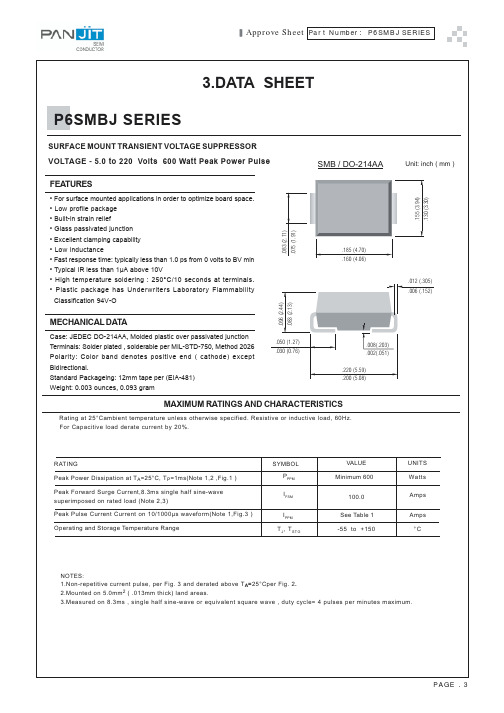
P6SMBJ SERIES 数据手册
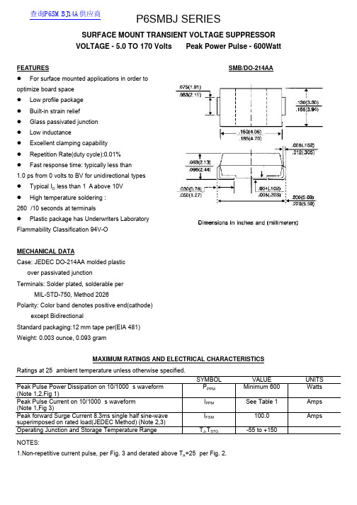
P6SMBJ SERIESSURFACE MOUNT TRANSIENT VOLTAGE SUPPRESSOR VOLTAGE - 5.0 TO 170 Volts Peak Power Pulse - 600WattFEATURESl For surface mounted applications in order to optimize board space l Low profile package l Built-in strain relief l Glass passivated junction l Low inductancel Excellent clamping capability l Repetition Rate(duty cycle):0.01% l Fast response time: typically less than 1.0 ps from 0 volts to BV for unidirectional types l Typical I D less than 1 A above 10V l High temperature soldering : 260 /10 seconds at terminalsl Plastic package has Underwriters Laboratory Flammability Classification 94V-OMECHANICAL DATACase: JEDEC DO-214AA molded plastic over passivated junctionTerminals: Solder plated, solderable per MIL-STD-750, Method 2026Polarity: Color band denotes positive end(cathode) except BidirectionalStandard packaging:12 mm tape per(EIA 481) Weight: 0.003 ounce, 0.093 gramMAXIMUM RATINGS AND ELECTRICAL CHARACTERISTICSRatings at 25 ambient temperature unless otherwise specified.SYMBOL VALUEUNITS Peak Pulse Power Dissipation on 10/1000 s waveform (Note 1,2,Fig 1)P PPM Minimum 600 Watts Peak Pulse Current on 10/1000 s waveform (Note 1,Fig 3)I PPM See Table 1 Amps Peak forward Surge Current 8.3ms single half sine-wave superimposed on rated load(JEDEC Method) (Note 2,3) I FSM 100.0 AmpsOperating Junction and Storage Temperature Range T J ,T STG-55 to +150NOTES:1.Non-repetitive current pulse, per Fig. 3 and derated above T A =25 per Fig.2. SMB/DO-214AA查询P6SMBJ14A供应商2.Mounted on 5.0mm2 (.013mm thick) land areas.3.Measured on 8 .3ms, single half sine-wave or equivalent square wave, duty cycle= 4 pulses per minutes maximum.MAXIMUM RATINGS AND CHARACTERISTIC CURVES P6SMBJ SERIESFig. 1-PEAK PULSE POWER RATING VERSUS Fig. 2-PULSE RATING CURVEFig. 3-PULSE WAVEFORM Fig. 4-TYPICAL JUNCTIONCAPACITANCENUMBER VRWM (V) MIN. @IT MAX. @IT (mA) @I PP VC (V) I PP (A) IR (uA)P6SMBJ5.0 P6SMBJ5.0A P6SMBJ6.0 P6SMBJ6.0A KDKEKFKG5.05.06.06.06.406.406.676.677.557.258.457.67101010109.69.211.410.362.565.252.658.3800800800800P6SMBJ6.5 P6SMBJ6.5A P6SMBJ7.0 P6SMBJ7.0A KHKKKLKM6.56.57.07.07.227.227.787.789.148.309.868.951010101012.311.213.312.048.753.645.150.0500500200200P6SMBJ7.5 P6SMBJ7.5A P6SMBJ8.0 P6SMBJ8.0A KNKPKQKR7.57.58.08.08.338.338.898.8910.679.5811.3010.23111114.312.915.013.642.046.540.044.11001005050P6SMBJ8.5 P6SMBJ8.5A P6SMBJ9.0 P6SMBJ9.0A KSKTKUKV8.58.59.09.09.449.4410.0010.0011.9210.8212.6011.50111115.914.416.915.437.741.735.539.0101055P6SMBJ10 P6SMBJ10A P6SMBJ11 P6SMBJ11A KWKXKYKZ10.010.011.011.011.1011.1012.2012.2014.1012.8015.4014.00111118.817.020.118.231.935.329.933.05555P6SMBJ12 P6SMBJ12A P6SMBJ13 P6SMBJ13A LDLELFLG12.012.013.013.013.3013.3014.4014.4016.9015.3018.2016.50111122.019.923.821.527.330.225.227.95555P6SMBJ14 P6SMBJ14A P6SMBJ15 P6SMBJ15A LHLKLLLM14.014.015.015.015.6015.6016.7016.7019.8017.9021.1019.20111125.823.226.924.423.325.822.324.05555P6SMBJ16 P6SMBJ16A P6SMBJ17 P6SMBJ17A LNLPLQLR16.016.017.017.017.8017.8018.9018.9022.6020.5023.9021.70111128.826.030.527.620.823.119.721.75555P6SMBJ18 P6SMBJ18A P6SMBJ20 P6SMBJ20A LSLTLULV18.018.020.020.020.0020.0022.2022.2025.3023.3028.1025.50111132.229.235.832.418.620.516.718.55555P6SMBJ22 P6SMBJ22A P6SMBJ24 P6SMBJ24A LWLXLYLZ22.022.024.024.024.4024.4026.7026.7030.9028.0033.8030.70111139.435.543.038.915.216.914.015.45555P6SMBJ26 P6SMBJ26A P6SMBJ28 P6SMBJ28A MDMEMFMG26.026.028.028.028.9028.9031.1031.1036.6033.2039.4035.80111146.642.150.045.412.414.212.013.25555P6SMBJ30 P6SMBJ30A P6SMBJ33 P6SMBJ33A MHMKMLMM30.030.033.033.033.3033.3036.7036.7042.2038.3046.5042.20111153.548.459.053.311.212.410.211.35555P6SMBJ36 P6SMBJ36A P6SMBJ40 P6SMBJ40A MNMPMQMR36.036.040.040.040.0040.0044.4044.4050.7046.0056.3051.10111164.358.171.464.59.310.38.49.35555P6SMBJ43 P6SMBJ43A P6SMBJ45 P6SMBJ45A MSMTMUMV43.043.045.045.047.8047.8050.0050.0060.5054.9063.3057.50111176.769.480.372.77.88.67.58.35555P6SMBJ48 P6SMBJ48A P6SMBJ51 P6SMBJ51A MWMXMYMZ48.048.051.051.053.3053.3056.7056.7067.5061.3071.8065.20111185.577.491.182.47.07.76.67.35555P6SMBJ54 P6SMBJ54A P6SMBJ58 P6SMBJ58A NDNENFNG54.054.058.058.060.0060.0064.4064.4076.0069.0081.6074.10111196.387.1103.093.66.26.95.86.45555P6SMBJ60 P6SMBJ60A P6SMBJ64 P6SMBJ64A NHNKNLNM60.060.064.064.066.7066.7071.1071.1084.5076.7090.1081.801111107.096.8114.0103.05.66.25.35.85555NUMBER VRWM (V) MIN. @IT MAX. @IT (mA) @I PP VC (V) I PP (A) IR (uA)P6SMBJ70 P6SMBJ70A P6SMBJ75 P6SMBJ75A NNNPNQNR70.070.075.075.077.8077.8083.3083.3098.6089.50105.7095.801111125.0113.0134.0121.04.85.34.54.95555P6SMBJ78 P6SMBJ78A P6SMBJ85 P6SMBJ85A NSNTNUNV78.078.085.085.086.7086.7094.4094.40109.8099.70119.20108.201111139.0126.0151.0137.04.34.73.94.45555P6SMBJ90P6SMBJ90A P6SMBJ100 P6SMBJ100A NWNXNYNZ90.090.0100.0100.0100.00100.00111.00111.00126.50115.50141.00128.001111160.0146.0179.0162.03.84.13.43.75555P6SMBJ110 P6SMBJ110A P6SMBJ120 P6SMBJ120A PDPEPFPG110.0110.0120.0120.0122.00122.00133.00133.00154.50140.50169.00153.001111196.0177.0214.0193.03.03.42.83.15555P6SMBJ130 P6SMBJ130A P6SMBJ150 P6SMBJ150A PHPKPLPM130.0130.0150.0150.0144.00144.00167.00167.00182.50165.50211.50192.501111231.0209.0268.0243.02.62.92.22.55555P6SMBJ160 P6SMBJ160A P6SMBJ170 P6SMBJ170A PNPPPQPR160.0160.0170.0170.0178.00178.00189.00189.00226.00205.00239.50217.501111287.0259.0304.0275.02.12.32.02.25555BI-DIRECTIONAL 600 Watt Surface Mount TVSBI-DIRECTIONALPARTNUMBERDEVICEMARKINGCODEREVERSESTAND-OFFVOLTAGEVRWM (V)BREAKDOWNVOLTAGEVBR (V)MIN. @ITBREAKDOWNVOLTAGEVBR (V)MAX. @ITTESTCURRENTIT(mA)MAXIMUMCLAMPINGVOLTAGE@I PP VC (V)PEAKPULSECURRENTI PP (A)REVERSELEAKAGE@VRWMIR (uA)P6SMBJ5.0C P6SMBJ5.0CA P6SMBJ6.0C P6SMBJ6.0CA ADAEAFAG5.05.06.06.06.406.406.676.677.557.258.457.67101010109.69.211.410.362.565.252.658.31600160016001600P6SMBJ6.5C P6SMBJ6.5CA P6SMBJ7.0C P6SMBJ7.0CA AHAKALAM6.56.57.07.07.227.227.787.789.148.309.868.951010101012.311.213.312.048.753.645.150.010001000400400P6SMBJ7.5C P6SMBJ7.5CA P6SMBJ8.0C P6SMBJ8.0CA ANAPAQAR7.57.58.08.08.338.338.898.8910.679.5811.3010.23111114.312.915.013.642.046.540.044.1200200100100P6SMBJ8.5C P6SMBJ8.5CA P6SMBJ9.0C P6SMBJ9.0CA ASATAUAV8.58.59.09.09.449.4410.0010.0011.9210.8212.6011.50111115.914.416.915.437.741.735.539.020201010P6SMBJ10C P6SMBJ10CA P6SMBJ11C P6SMBJ11CA AWAXAYAZ10.010.011.011.011.1011.1012.2012.2014.1012.8015.4014.00111118.817.020.118.231.935.329.933.05555P6SMBJ12C P6SMBJ12CA P6SMBJ13C P6SMBJ13CA BDBEBFBG12.012.013.013.013.3013.3014.4014.4016.9015.3018.2016.50111122.019.923.821.527.330.225.227.95555P6SMBJ14C P6SMBJ14CA P6SMBJ15C P6SMBJ15CA BHBKBLBM14.014.015.015.015.6015.6016.7016.7019.8017.9021.1019.20111125.823.226.924.423.325.822.324.05555P6SMBJ16C P6SMBJ16CA P6SMBJ17C P6SMBJ17CA BNBPBQBR16.016.017.017.017.8017.8018.9018.9022.6020.5023.9021.70111128.826.030.527.620.823.119.721.75555P6SMBJ18C P6SMBJ18CA P6SMBJ20C P6SMBJ20CA BSBTBUBV18.018.020.020.020.0020.0022.2022.2025.3023.3028.1025.50111132.229.235.832.418.620.516.718.55555P6SMBJ22C P6SMBJ22CA P6SMBJ24C P6SMBJ24CA BWBXBYBZ22.022.024.024.024.4024.4026.7026.7030.9028.0033.8030.70111139.435.543.038.915.216.914.015.45555P6SMBJ26C P6SMBJ26CA CDCE26.026.028.9028.9036.6033.201146.642.112.414.255P6SMBJ28C P6SMBJ28CA CFCG28.028.031.1031.1039.4035.801150.045.412.013.255P6SMBJ30C P6SMBJ30CA P6SMBJ33C P6SMBJ33CA CHCKCLCM30.030.033.033.033.3033.3036.7036.7042.2038.3046.5042.20111153.548.459.053.311.212.410.211.35555P6SMBJ36C P6SMBJ36CA P6SMBJ40C P6SMBJ40CA CNCPCQCR36.036.040.040.040.0040.0044.4044.4050.7046.0056.3051.10111164.358.171.464.59.310.38.49.35555P6SMBJ43C P6SMBJ43CA P6SMBJ45C P6SMBJ45CA CSCTCUCV43.043.045.045.047.8047.8050.0050.0060.5054.9063.3057.50111176.769.480.372.77.88.67.58.35555P6SMBJ48C P6SMBJ48CA P6SMBJ51C P6SMBJ51CA CWCXCYCZ48.048.051.051.053.3053.3056.7056.7067.5061.3071.8065.20111185.577.491.182.47.07.76.67.35555P6SMBJ54C P6SMBJ54CA P6SMBJ58C P6SMBJ58CA DDDEDFDG54.054.058.058.060.0060.0064.4064.4076.0069.0081.6074.10111196.387.1103.093.66.26.95.86.45555P6SMBJ60C P6SMBJ60CA P6SMBJ64C P6SMBJ64CA DHDKDLDM60.060.064.064.066.7066.7071.1071.1084.5076.7090.1081.801111107.096.8114.0103.05.66.25.35.85555BI-DIRECTIONAL 600 Watt Surface Mount TVSBI-DIRECTIONALPARTNUMBERDEVICEMARKINGCODEREVERSESTAND-OFFVOLTAGEVRWM (V)BREAKDOWNVOLTAGEVBR (V)MIN. @ITBREAKDOWNVOLTAGEVBR (V)MAX. @ITTESTCURRENTIT(mA)MAXIMUMCLAMPINGVOLTAGE@I PP VC (V)PEAKPULSECURRENTI PP (A)REVERSELEAKAGE@VRWMIR (uA)P6SMBJ70C P6SMBJ70CA P6SMBJ75C P6SMBJ75CA DNDPDQDR70.070.075.075.077.8077.8083.3083.3098.6089.50105.7095.801111125.0113.0134.0121.04.85.34.54.95555P6SMBJ78C P6SMBJ78CA P6SMBJ85C P6SMBJ85CA DSDTDUDV78.078.085.085.086.7086.7094.4094.40109.8099.70119.20108.201111139.0126.0151.0137.04.34.73.94.45555P6SMBJ90CP6SMBJ90CA P6SMBJ100C P6SMBJ100CA DWDXDYDZ90.090.0100.0100.0100.00100.00111.00111.00126.50115.50141.00128.001111160.0146.0179.0162.03.84.13.43.75555P6SMBJ110C P6SMBJ110CA P6SMBJ120C P6SMBJ120CA EDEEEFEG110.0110.0120.0120.0122.00122.00133.00133.00154.50140.50169.00153.001111196.0177.0214.0193.03.03.42.83.15555P6SMBJ130C P6SMBJ130CA P6SMBJ150C P6SMBJ150CA EHEKELEM130.0130.0150.0150.0144.00144.00167.00167.00182.50165.50211.50192.501111231.0209.0268.0243.02.62.92.22.55555P6SMBJ160C P6SMBJ160CA P6SMBJ170C P6SMBJ170CA ENEPEQER160.0160.0170.0170.0178.00178.00189.00189.00226.00205.00239.50217.501111287.0259.0304.0275.02.12.32.02.25555。
MAC6中文说明书
3-3 订货信息
项目 型号 输入
代码 MAC6A-
调节输出 1
电源
规格 96×96mm 5 位数字显示高精度字控制器 M 自由输入、TC、RTD、mV、V、mA
C 继电器接点 1a 240V AC 2A( 阻性负载 ) S 固态继电器(SSR)驱动 12V DC 最大20mA I 电流 4-20mA DC 负载电阻最大500Ω V 电压 0-10V DC 负载电流最大2mA Y 控制电机 (伺服控制输出)接点容量1C 240V AC 2A X 控制电机 (伺服控制输出)SSR 240V AC 2A
3
生电磁干扰。请在采取有效措施后使用。 ● 仪器具有用于散热的通风口,并且确保金属不会进入通风口中,否则会引起故障或者火灾。 ● 不要阻塞通风口或者使尘埃和其他类似物附着在上面,温度升高或者绝缘失效都会缩短产品寿命并
引起火灾。 ● 应该注意在重复性极限值(如电压、噪声、浪涌)实验时可能会损坏设备。 ● 禁止使用者改型和不正当使用。 3 简介 3-1 使用前的检查
在使用 MAC6 前请检查型号代码、外观和附件。确认没有错误、损坏和丢失。 确认型号代码,检查与订货的产品一致。根据下述代码表检查机壳上的型号代码。 检查附件 「注」 如果您有任何问题请联系我们的代理商或者营业本部。我们欢迎任何询问,例如,产品缺
陷、附件丢失等。
「 注意 」
3-2 使用注意事项 ●不要用硬的、尖的物体操作前面板。不要用指甲尖触碰按键。 ●当清洁仪器时,用干布轻擦。不要使用溶剂,如,稀释剂。
7. 功能的补充说明・・・・・・・・・・・・・・・・・・・・・・・・・・・・・・・・・・・・・・・・・・・・・・・・・・・・・・・・・・・・・・・60
7-1 自动返回功能・・・・・・・・・・・・・・・・・・・・・・・・・・・・・・・・・・・・・・・・・・・・・・・・・・・・・・・・・・・・・60 7-2 输出软启动功能・・・・・・・・・・・・・・・・・・・・・・・・・・・・・・・・・・・・・・・・・・・・・・・・・・・・・・・・・・・60 7-3 事件报警方式・・・・・・・・・・・・・・・・・・・・・・・・・・・・・・・・・・・・・・・・・・・・・・・・・・・・・・・・・・・・・60 7-4 AT(自整定)・・・・・・・・・・・・・・・・・・・・・・・・・・・・・・・・・・・・・・・・・・・・・・・・・・・・・・・・・・・・・60
低功耗瞬态管P6SMB15CA型号说明

低功耗瞬态管P6SMB15CA型号说明硕凯电子(Sylvia)一、最大额定值Notes:1.Non-repetitive current pulse,per Fig.3and derated above TA=25°C per Fig.2.2.Mounted on5.0mm x5.0mm(0.03mm thick)Copper Pads to each terminal.3.8.3ms single half sine-wave,or equivalent square wave,Duty cycle=4pulses per minutes maximum.4.VF<3.5V for VBR<200V and VF<6.5V for VBR>201V.二、脉冲浪涌三、UL认证编号四、产品应用说明TVS器件非常适合保护I/O接口,Vcc总线和其他应用于电信、计算机、工业和消费电子应用的易损电路。
五、脉冲降额曲线五、电路图六、I-V曲线特性七、产品特性1、为表面安装应用优化电路板空间2、低泄漏3、单向和双向单元4、玻璃钝化结5、低电感6、优良的钳位能力7、600W的峰值功率能力在10×1000μ波形重复率(占空比):0.01%8、快速响应时间:从0伏特到最小击穿电压通常小于1.0ps9、典型的,在电压高于12V时,反向漏电流小于5μA10、高温焊接:终端260°C/40秒11、典型的最大温度系数△Vbr=0.1%x Vbr@25°C x△T12、塑料包装有保险商实验室可燃性94V-013、无铅镀雾锡14、无卤化,符合RoHS15、典型失效模式是在指定的电压或电流下出现16、晶须测试是基于JEDEC JESD201A每个表4a及4c进行的17、IEC-61000-4-2ESD15kV(空气),8kV(接触)18、数据线的ESD保护符合IEC61000-4-2(IEC801-2)19、数据线的EFT保护符合IEC61000-4-4(IEC801-4)八、瞬态管产品图。
- 1、下载文档前请自行甄别文档内容的完整性,平台不提供额外的编辑、内容补充、找答案等附加服务。
- 2、"仅部分预览"的文档,不可在线预览部分如存在完整性等问题,可反馈申请退款(可完整预览的文档不适用该条件!)。
- 3、如文档侵犯您的权益,请联系客服反馈,我们会尽快为您处理(人工客服工作时间:9:00-18:30)。
#
#6EJ#; #%I;5
#
,'
$
/
0 K<8
46 ;M 46 ;M* 46 =;5 46 =;5* 46 M; 46 M;* 46 !;2 46 !;2* 46 2 46 2* 46 22 46 22* 46 2 46 2* 46 2> 46 2>* 46 25 46 25* 46 2 46 2* 46 2M 46 2M* 46 46 * 46 46 * 46 " 46 "* 46 = 46 =* 46 > 46 >* 46 >> 46 >>* 46 > 46 >* 46 >! 46 >!* 46 ">
,
<,
* 2 2 2 2 2 2 2 2 2 2 2 2 2 2 2 2 2 2 2 2 2 2 2 2 2 2 2 2 2 2 2 2 2 2 2 2 2 2 2
0 /
0 K<
#
<
#
*
2;M
5M
2;5
22;=
5>
22;>
/
0 K<8
#:
<8
#
L*
46 ">*
>;M
5
46 "=
>M;2
5
46 "=*
";
5
46 52
"2;>
5
46 52*
">;
5
46 5
"5;"
5
46 5*
"=;M
5
46
5;
5
46 *
5>
5
46 M
;2 0 ,
& <$4,8$=5
0
' 4 -0 0 >
1) ?
$ / / < @ (+
2"5
5
46 2M
2"
5
46 2M*
25"
5
46
2
5
46 *
2=2
5
46
2=5
5
46 *
2M5
5
46 5"+
5
46 5*"+
2"
5
46 >"+
">
5
46 >*"+
5
>M
#
"5; 52;= "!;" 5;2 5>; 2; 5M;M M; 5;2 =";M =2;" M;5 =M;M !; M;2 2 !5;5 22 25 22 22 2> 2 2"> 2>= 25 25M 2= 2M 2M= 2=! 2!M 2M! 2 " >2 =5 > >> >25 >M5 >M ""
25
G7:
,F
9 0 F
,
4
0
#
. /
0 < @ 5 * >+
$ 5 H 25
$ 5 H 25
#6EI#; #%I>;
元器件交易网
P6 SMB 6,8 ... P6 SMB 400CA
Surface mount diode
Unidirectional and Bidirectional Transient Voltage Suppressor diodes
P6 SMB 6,8 ... P6 SMB 400CA Pulse Power Dissipation: 600 W Maximum Stand-off voltage: 5,5 ... 342 V
!;
";M
!;=
=>;5
M;5
=;2
M;!
M;5
=;M
==
M;2
M!
=
M5
=;"
!M
;"
!
;M
2M
5;M
2>
;2
22M
5;>
22>
5;5
2>2
";M
25
5
2""
";>
2>=
";5
25M
>;!
25
";2
2=>
>;
25
>;M
2M=
>;>
2=!
>;5
25
;!
=
>
>
;=
2)
&
. 5
3)
' 4) 6
'
1
Absolute Maximum Ratings Symbol Conditions
P6 SMB 6,8 ... P6 SMB 400CA
46 7 89$2"**
Fig. 1 10/1000 µs - pulse waveform
Fig. 2 Rated power dissipation vs. ambient temp. 2)
Fig. 3 Peak pulse power versus pulse duration
,
& -
. /
0
' 123 4 )*)
153
& -
. /
0
Mechanical Data 46 7 89$2"** : 0
! !;5 !;! 2;5 2;M 22;" 22;= 2;" 2>;5 2";> 2";" 25; 2; 2=;2 2M 2! 2!;M ;! 2; ;M ";> 5;= = M;5 !;= >2;" >;" >"; >5;2 >=;2 >M;=
#
=;"M =;2" M;5 =;MM !; M;2 2 !;55 22 2;5 2;2 22; 2>; 2; 2";> 2>;= 2;5 25;M 2=; 2;M 2!;M 2M;! 2 "; >;2 ;" 5; !;= M;" >> >2;5 >;> >";= >!; >=;M ";! "2 "=;>
"
,
<,
* 2 2 2 2 2 2 2 2 2 2 2 2 2 2 2 2 2 2 2 2 2 2 2 2 2 2 2 2 2 2 2 2 2 2 2 2 2 2 2 2 2 2 2 2
2
0 /
0 K<
#
<
#
*
5!;>
2;
=;M
Features
!"#$
%
&
' ( ))
)*)+ ' &
3
12-03-2007 MAM
© by SEMIKRON
2;M
">;5
2"ຫໍສະໝຸດ "2;"25
"=;=
2>
"5;=
2>;M
5
2
"!;!
2;
5;"
22;2
5>;!
22;
2;!
2
© by SEMIKRON
元器件交易网
P6 SMB 6,8 ... P6 SMB 400CA
,'
$
,* @ 5 ;
.
Values
Units
-
.
272 B ./
2+ , @ 5
:
(*#+
4 '
.
+; , @ 5
2!
;M
""
;5
>"
;
5M
;"
"
;5
M=
;2
="
;
>""
2;=
>M
2;M
>
2;=
>""
2;=
">
2;"
"2"
2;"
5"
2;
"M
2;
5="
2
5"M