BAV70-7-F;BAV70-7;BAV70TA;中文规格书,Datasheet资料
BAV70中文资料_数据手册_参数

H E 2.10
T
0°
2.40 −−−
2.64 10°
MIN 0.035 0.000 0.015 0.003 0.110 0.047 0.070 0.012 0.014
0.083 0°
INCHES
NOM 0.039 0.002 0.017 0.006 0.114 0.051 0.075 0.017 0.021 0.094 −−−
820 W
+10 V
2.0 k 100 mH IF 0.1 mF
50 W OUTPUT PULSE
GENERATOR
D.U.T.
0.1 mF
tr
tp
t
10%
50 W INPUT
SAMPLING
VR
OSCILLOSCOPE
90% INPUT SIGNAL
IF
trr
t
iR(REC) = 1.0 mA IR
SOT−23 (TO−236) CASE 318 STYLE 9
3 CATHODE
ANODE 1
2 ANODE
MARKING DIAGRAM
A4 M G G
1
A4 = Device Code M = Date Code* G = Pb−Free Package
(Note: Microdot may be in either location) *Date Code orientation and/or overbar may
Figure 3. Leakage Current
0.6
0.58
0.56
0.54
0.52
0.5
0.48
0
1
BAV70LT1中文资料
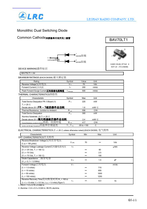
LESHAN RADIO COMPANY, LTD. Monolithic Dual Switching DiodeCommon Cathode共阴极单片双开关二极管3CATHODE阴极DEVICE MARKING器件标识BAV70LT131ANODE阳极 12 2ANODE阳极CASE 318-08, STYLE 9SOT-23 (TO-236AB)BAV70LT1 = A4MAXIMUM RATINGS (EACH DIODE) 最大额定值Rating Symbol Value Unit Reverse Voltage反向电压V R 70 VdcForward Current正向电流I F 200 mAdcPeak Forward Surge Current正向浪涌电流峰值I FM(surge) 500 mAdcTHERMAL CHARACTERISTICS热特性Characteristic Symbol Max Unit Total Device Dissipation FR- 5 Board (1) P D 225 mWT A = 25°CDerate above 25°C FR – 5板的器件总功耗 1.8 mW/°CThermal Resistance, Junction to Ambient R θJA 556 °C/WTotal Device Dissipation P D 300 mWAlumina Substrate, (2) T A = 25°CDerate above 25°C氧化铝基板的器件总功耗 2.4 mW/°CThermal Resistance, Junction to Ambient热阻,结到环境R θJA 417 °C/WJunction and Storage Temperature结温和存储温度T J , T stg -55 to +150 °CELECTRICAL CHARACTERISTICS (T A = 25°C unless otherwise noted) (EACH DIODE)电气特性Characteristic Symbol Min Max Unit OFF CHARACTERISTICS开关特性Reverse Breakdown Voltage反向击穿电压(I (BR) = 100 µAdc)Reverse Voltage Leakage Current反向漏电流电压(V R = 25 Vdc, T J = 150°C)(V R = 70 Vdc)(V R = 70 Vdc, T J = 150°C)Diode Capacitance二极管电容(V R = 0, f = 1.0 MHz) V (BR) 70 —VdcI R µAdc—60— 2.5—100C D — 1.5 pFForward Voltage正向电压(I F = 1.0 mAdc)(I F = 10 mAdc)(I F = 50 mAdc)(I F = 150 mAdc)Reverse Recovery Time反向恢复时间 R L = 100 Ω(I F = I R = 10 mAdc, V R = 5.0 Vdc, I R(REC) = 1.0 mAdc) (Figure 1) V F mVdc—715—855—1000—1250t rr — 6.0 ns1. FR-5 = 1.0 x 0.75 x 0.062 in.2. Alumina = 0.4 x 0.3 x 0.024 in. 99.5% alumina.G5-1/1。
BAV70;BAV74;BAV70_D87Z;BAV74_D87Z;中文规格书,Datasheet资料

BAV70 / 74Small Signal DiodeAbsolute Maximum Ratings * T A= 25°C unless otherwise noted* These ratings are limiting values above which the serviceability of the diode may be impaired.NOTES:1)These ratings are based on a maximum junction temperature of 150 degrees C.2)These are steady limits. The factory should be consulted on applications involving pulsed or low duty cycle operations.Thermal CharacteristicsElectrical Characteristics T A=25°C unless otherwise notedSymbol ParameterValue Units V RRM Maximum Repetitive Reverse Voltage BAV70BAV747050V V I F(AV)Average Rectified Forward Current 200mA I FSMNon-repetitive Peak Forward Surge CurrentPulse Width = 1.0 secondPulse Width = 1.0 microsecond 1.02.0A A T STG Storage Temperature Range -55 to +150°C T JOperating Junction Temperature150°CSymbol ParameterValue Units P D Power Dissipation350mW R θJAThermal Resistance, Junction to Ambient357°C/WSymbol ParameterTest ConditionsMin.Max.Units V R Breakdown Voltage BAV70BAV74I R = 100µA I R = 5.0µA 7550V V V FForward Voltage BAV70BAV74I F = 1.0mA I F = 10mA I F = 50mA I F = 150mA I F = 100mA7158551.01.251.0mV mV V V V I RReverse Leakage BAV70BAV74V R = 25V, T A = 150°C V R = 70VV R = 70V, T A = 150°C V R = 50VV R = 50V, T A = 150°C 605.010*******µA µA µA nA µA C T Total Capacitance BAV70BAV74V R = 0V, f = 1.0MHz V R = 0V, f = 1.0MHz1.52.0pF pF t rrReverse Recovery Time BAV70BAV74I F = I R = 10mA, I RR = 1.0mA, R L = 100ΩI F = I R = 10mA, I RR = 1.0mA, R L = 100Ω6.04.0ns nsBAV70 / 74Connection Diagram123A4123SOT-23312BAV70 A4 BAV74 JAMARKINGDISCLAIMERFAIRCHILD SEMICONDUCTOR RESERVES THE RIGHT TO MAKE CHANGES WITHOUT FURTHER NOTICE TO ANY PRODUCTS HEREIN TO IMPROVE RELIABILITY, FUNCTION OR DESIGN. FAIRCHILD DOES NOT ASSUME ANY LIABILITY ARISING OUT OF THE APPLICATION OR USE OF ANY PRODUCT OR CIRCUIT DESCRIBED HEREIN;NEITHER DOES IT CONVEY ANY LICENSE UNDER ITS PATENT RIGHTS, NOR THE RIGHTS OF OTHERS.LIFE SUPPORT POLICYFAIRCHILD’S PRODUCTS ARE NOT AUTHORIZED FOR USE AS CRITICAL COMPONENTS IN LIFE SUPPORT DEVICES OR SYSTEMS WITHOUT THE EXPRESS WRITTEN APPROVAL OF FAIRCHILD SEMICONDUCTOR CORPORATION.As used herein:1. Life support devices or systems are devices or systems which, (a) are intended for surgical implant into the body,or (b) support or sustain life, or (c) whose failure to perform when properly used in accordance with instructions for use provided in the labeling, can be reasonably expected to result in significant injury to the user.2. A critical component is any component of a life support device or system whose failure to perform can be reasonably expected to cause the failure of the life support device or system, or to affect its safety or effectiveness.PRODUCT STATUS DEFINITIONS Definition of TermsDatasheet Identification Product Status DefinitionAdvance InformationFormative or In Design This datasheet contains the design specifications for product development. Specifications may change in any manner without notice.PreliminaryFirst ProductionThis datasheet contains preliminary data, andsupplementary data will be published at a later date.Fairchild Semiconductor reserves the right to make changes at any time without notice in order to improve design.No Identification Needed Full ProductionThis datasheet contains final specifications. Fairchild Semiconductor reserves the right to make changes at any time without notice in order to improve design.Obsolete Not In ProductionThis datasheet contains specifications on a product that has been discontinued by Fairchild semiconductor.The datasheet is printed for reference information only.TRADEMARKSThe following are registered and unregistered trademarks Fairchild Semiconductor owns or is authorized to use and is not intended to be an exhaustive list of all such trademarks.FAST ®FASTr™FPS™FRFET™GlobalOptoisolator™GTO™HiSeC™I 2C™i-Lo ™ImpliedDisconnect™ISOPLANAR™LittleFET™MICROCOUPLER™MicroFET™MicroPak™MICROWIRE™MSX™MSXPro™OCX™OCXPro™OPTOLOGIC ®OPTOPLANAR™PACMAN™POP™Power247™PowerEdge™PowerSaver™PowerTrench ®QFET ®QS™QT Optoelectronics™Quiet Series™RapidConfigure™RapidConnect™µSerDes™SILENT SWITCHER ®SMART START™SPM™Stealth™SuperFET™SuperSOT™-3SuperSOT™-6SuperSOT™-8SyncFET™TinyLogic ®TINYOPTO™TruTranslation™UHC™UltraFET ®VCX™A CEx™ActiveArray™Bottomless™CoolFET™CROSSVOLT ™DOME™EcoSPARK™E 2CMOS™EnSigna™FACT™FACT Quiet Series™Across the board. Around the world.™The Power Franchise ®Programmable Active Droop™分销商库存信息:FAIRCHILDBAV70BAV74BAV70_D87Z BAV74_D87Z。
BAV70,215;BAV70,235;BAV70T,115;BAV70W,135;BAV70W,115;中文规格书,Datasheet资料

1.Product profile1.1General descriptionHigh-speed switching diodes, encapsulated in small Surface-Mounted Device (SMD)plastic packages.1.2Features1.3ApplicationsI High-speed switchingI General-purpose switching1.4Quick reference data[1]When switched from I F =10mA to I R =10mA; R L =100Ω; measured at I R =1mA.BAV70 seriesHigh-speed switching diodesRev. 07 — 27 November 2007Product data sheetTable 1.Product overviewType numberPackage PackageconfigurationConfiguration NXPJEITA JEDEC BAV70SOT23-TO-236AB smalldual common cathode BAV70M SOT883SC-101-leadless ultra small dual common cathode BAV70S SOT363SC-88-very small quadruple commoncathode/common cathode BAV70T SOT416SC-75-ultra small dual common cathode BAV70WSOT323SC-70-very smalldual common cathodeI High switching speed: t rr ≤4ns I Low capacitance: C d ≤1.5pF I Low leakage currentI Reverse voltage: V R ≤100VI Small SMD plastic packagesTable 2.Quick reference data Symbol Parameter Conditions Min Typ Max Unit Per diode I R reverse current V R =80V--0.5µA V R reverse voltage --100V t rrreverse recovery time[1]--4ns2.Pinning information3.Ordering informationTable 3.PinningPin Description Simplified outline SymbolBAV70; BAV70T; BAV70W1anode (diode 1)2anode (diode 2)3common cathodeBAV70M 1anode (diode 1)2anode (diode 2)3common cathodeBAV70S 1anode (diode 1)2anode (diode 2)3common cathode (diode 3and diode 4)4anode (diode 3)5anode (diode 4)6common cathode (diode 1and diode2)006aaa144123006aab034132312Transparent top view006aab034132132456006aab104136254Table 4.Ordering informationType numberPackage NameDescriptionVersion BAV70-plastic surface-mounted package; 3leadsSOT23BAV70M SC-101leadless ultra small plastic package; 3solder lands;body 1.0×0.6×0.5mmSOT883BAV70S SC-88plastic surface-mounted package; 6leads SOT363BAV70T SC-75plastic surface-mounted package; 3leads SOT416BAV70WSC-70plastic surface-mounted package; 3leadsSOT3234.Marking[1]* = -: made in Hong Kong * = p: made in Hong Kong * = t: made in Malaysia * = W: made in China5.Limiting valuesTable 5.Marking codesType numberMarking code [1]BAV70A4*BAV70M S4BAV70S A4*BAV70T A4BAV70WA4*Table 6.Limiting valuesIn accordance with the Absolute Maximum Rating System (IEC 60134).Symbol Parameter Conditions Min Max Unit Per diode V RRM repetitive peak reverse voltage -100V V R reverse voltage -100V I Fforward current BAV70T amb ≤25°C -215mA BAV70M T s =90°C -150mA BAV70S T s =60°C -250mA BAV70T T s =90°C -150mA BAV70WT amb ≤25°C-175mAI FRMrepetitive peak forward current BAV70-450mA BAV70M -500mA BAV70S -450mA BAV70T -500mA BAV70W-500mA I FSMnon-repetitive peak forward current square wave [1]t p =1µs-4A t p =1ms -1A t p =1s-0.5A[1]T j =25°C prior to surge.[2]Device mounted on an FR4Printed-Circuit Board (PCB), single-sided copper, tin-plated and standard footprint.[3]Reflow soldering is the only recommended soldering method.6.Thermal characteristics[1]Device mounted on an FR4PCB, single-sided copper, tin-plated and standard footprint.[2]Reflow soldering is the only recommended soldering method.P tottotal power dissipation [2]BAV70T amb ≤25°C -250mW BAV70M T amb ≤25°C [3]-250mW BAV70S T s =60°C -350mW BAV70T T s =90°C -170mW BAV70WT amb ≤25°C-200mWPer device I Fforward current BAV70T amb ≤25°C -125mA BAV70M T s =90°C -75mA BAV70S T s =60°C -100mA BAV70T T s =90°C -75mA BAV70WT amb ≤25°C-100mA T j junction temperature -150°C T amb ambient temperature −65+150°C T stgstorage temperature−65+150°CTable 6.Limiting values …continuedIn accordance with the Absolute Maximum Rating System (IEC 60134).Symbol ParameterConditionsMin Max Unit Table 7.Thermal characteristics Symbol ParameterConditions Min Typ Max UnitPer diode R th(j-a)thermal resistance from junction to ambient in free air[1]BAV70--500K/W BAV70M [2]--500K/W BAV70W--625K/WR th(j-t)thermal resistance from junction to tie-point BAV70--360K/W BAV70W--300K/WR th(j-sp)thermal resistance from junction to solder point BAV70S --255K/W BAV70T--350K/W7.CharacteristicsTable 8.CharacteristicsT amb=25°C unless otherwise specified.Symbol Parameter Conditions Min Typ Max UnitPer diodeV F forward voltage[1]I F=1mA--715mVI F=10mA--855mVI F=50mA--1VI F=150mA-- 1.25VI R reverse current V R=25V--30nAV R=80V--0.5µAV R=25V;T j=150°C--30µAV R=80V;T j=150°C--100µAC d diode capacitance V R=0V; f=1MHz-- 1.5pFt rr reverse recovery time[2]--4nsV FR forward recovery voltage[3]-- 1.75V[1]Pulse test: t p≤300µs;δ≤0.02.[2]When switched from I F=10mA to I R=10mA; R L=100Ω; measured at I R=1mA.[3]When switched from I F=10mA; t r=20ns.(1)T amb =150°C (2)T amb =85°C (3)T amb =25°C (4)T amb =−40°CBased on square wave currents.T j =25°C; prior to surgeFig 1.Forward current as a function of forwardvoltage; typical valuesFig 2.Non-repetitive peak forward current as afunction of pulse duration; maximum values(1)T amb =150°C (2)T amb =85°C (3)T amb =25°C (4)T amb =−40°Cf =1MHz; T amb =25°CFig 3.Reverse current as a function of reversevoltage; typical values Fig 4.Diode capacitance as a function of reversevoltage; typical values006aab107V F (V)0.21.41.00.6110102103I F (mA)10−1(1)(2)(3)(4)mbg704101102I FSM (A)10−1t p (µs)110410310102006aab10810−210−410−310110−1102I R (µA)10−5V R (V)10080406020(1)(2)(3)(4)08161240.80.60.40.2mbg446V R (V)C d (pF )8.Test information(1)I R =1mAInput signal: reverse pulse rise time t r =0.6ns; reverse voltage pulse duration t p =100ns; duty cycle δ=0.05Oscilloscope: rise time t r =0.35nsFig 5.Reverse recovery time test circuit and waveformsInput signal: forward pulse rise time t r =20ns; forward current pulse duration t p ≥100ns; duty cycle δ≤0.005Fig 6.Forward recovery voltage test circuit and waveformst rr(1)+ I Ftoutput signalt rt pt10 %90 %V Rinput signal V = V R + I F × R SR S = 50 ΩI FD.U.T.R i = 50 ΩSAMPLING OSCILLOSCOPEmga881t rtt p 10 %90 %Iinput signalR S = 50 ΩIR i = 50 ΩOSCILLOSCOPE1 k Ω450 ΩD.U.T.mga882V FRtoutput signalV9.Package outlineFig 7.Package outline BAV70(SOT23/TO-236AB)Fig 8.Package outline BAV70M (SOT883/SC-101)Fig 9.Package outline BAV70S (SOT363/SC-88)Fig 10.Package outline BAV70T (SOT416/SC-75)Fig 11.Package outline BAV70W (SOT323/SC-70)04-11-04Dimensions in mm0.450.151.91.10.93.02.82.52.1 1.41.20.480.380.150.0912303-04-03Dimensions in mm0.620.550.550.470.500.460.650.200.123210.300.220.300.221.020.950.3506-03-16Dimensions in mm0.250.100.30.2pin 1index1.30.652.22.0 1.351.152.21.8 1.10.80.450.1513246504-11-04Dimensions in mm0.950.601.81.41.751.450.90.70.250.1010.300.151230.450.1504-11-04Dimensions in mm0.450.151.10.82.21.82.22.0 1.351.151.30.40.30.250.1012310.Packing information[1]For further information and the availability of packing methods, see Section 14.[2]T1: normal taping [3]T2: reverse taping11.SolderingTable 9.Packing methodsThe indicated -xxx are the last three digits of the 12NC ordering code.[1]Type number Package DescriptionPacking quantity 300010000BAV70SOT234mm pitch, 8mm tape and reel -215-235BAV70M SOT8832mm pitch, 8mm tape and reel --315BAV70S SOT3634mm pitch, 8mm tape and reel; T1[2]-115-1354mm pitch, 8mm tape and reel; T2[3]-125-165BAV70T SOT4164mm pitch, 8mm tape and reel -115-135BAV70WSOT3234mm pitch, 8mm tape and reel-115-135Fig 12.Reflow soldering footprint BAV70(SOT23/TO-236AB)solder resistoccupied areasolder landssolder paste Dimensions in mmsot0231.000.60(3x)1.301232.503.000.85 2.702.900.50 (3x)0.60 (3x)3.300.85Fig 13.Wave soldering footprint BAV70(SOT23/TO-236AB)Reflow soldering is the only recommended soldering method.Fig 14.Reflow soldering footprint BAV70M (SOT883/SC-101)sot0234.004.60 2.804.501.203.403211.20 (2x)preferred transport direction during solderingDimensions in mmsolder resist occupied areasolder lands solder lands solder pastesolder resist occupied areaDimensions in mm1.300.30R = 0.05 (12×)R = 0.05 (12×)0.600.700.800.900.30(2×)0.35(2×)0.200.40(2×)0.50(2×)0.25(2×)0.300.400.50分销商库存信息:NXPBAV70,215BAV70,235BAV70T,115 BAV70W,135BAV70W,115BAV70S,115 BAV70M,315BAV70S,135。
MCC BAV70WT 电路切换二极管数据手册说明书

BAV70WT
Packing Tape&Reel: 3Kpcs/Reel
***IMPORTANT NOTICE***
Micro Commercial Components Corp UHVHUYHV WKH ULJKW WR PDNH FKDQJHV ZLWKRXW IXUWKHU QRWLFH WR DQ\ SURGXFW KHUHLQ WR PDNH FRUUHFWLRQV PRGLILFDWLRQV HQKDQFHPHQWV LPSURYHPHQWV RU RWKHU FKDQJHV Micro Commercial Components Corp GRHV QRW DVVXPH DQ\ OLDELOLW\ DULVLQJ RXW RI WKH DSSOLFDWLRQ RU XVH RI DQ\ SURGXFW GHVFULEHG KHUHLQ QHLWKHU GRHV LW FRQYH\DQ\OLFHQVHXQGHULWVSDWHQWULJKWVQRUWKHULJKWVRIRWKHUV7KHXVHURISURGXFWVLQVXFKDSSOLFDWLRQVVKDOODVVXPHDOO ULVNVRIVXFKXVHDQGZLOODJUHHWRKROGMicro Commercial Components CorpDQGDOOWKHFRPSDQLHVZKRVHSURGXFWVDUH UHSUHVHQWHGRQRXUZHEVLWHKDUPOHVVDJDLQVWDOOGDPDJHV0LFUR&RPPHUFLDO&RPSRQHQWV&RUSSURGXFWVDUHVROGVXEMHFW WRWKHJHQHUDOWHUPVDQGFRQGLWLRQVRIFRPPHUFLDOVDOHDVSXEOLVKHGDW KWWSVZZZPFFVHPLFRP+RPH7HUPV$QG&RQGLWLRQV
BAV70-V中文资料

BAV70-VDocument Number 85546 Rev. 1.7, 09-Mar-06Vishay Semiconductors1Small Signal Switching Diode, DualFeatures•Silicon Epitaxial Planar Diode•Fast switching dual diode with commoncathode•This diode is also available in other con-figurations including:a dual common anode tocathode with type designation BAV99-V, a dualcommon anode with type designation BAW56-V,and a single diode with type designation BAL99-V. •Lead (Pb)-free component•Component in accordance to RoHS 2002/95/EC and WEEE 2002-96/ECMechanical Data Case: SOT23 Plastic case Weight: approx. 8.8 mg Packaging Codes/Options:GS18 / 10 k per 13" reel (8 mm tape), 10 k/box GS08 / 3 k per 7" reel (8 mm tape), 15 k/boxParts TableAbsolute Maximum Ratings T amb = 25°C, unless otherwise specified 1) Device on fiberglass substrate, see layoutPart Ordering code Marking Remarks BAV70-V BAV70-V-GS18 or BAV70-V-GS08JJ T ape and ReelParameter T est condition Symbol Value Unit Reverse voltage, peak reversevoltageV R, V RM70V Forward current (continuous)I F250mA Non repetitive peak forwardcurrentt p = 1 µs I FSM2At p = 1 ms I FSM1At p = 1 s I FSM0.5A Power dissipation P tot3501)mW 2Document Number 85546Rev. 1.7, 09-Mar-06BAV70-VVishay Semiconductors Thermal CharacteristicsT amb = 25°C, unless otherwise specified1)Device on Fiberglass substrate, see layout on second page.Electrical CharacteristicsT amb = 25°C, unless otherwise specifiedTypical CharacteristicsT amb = 25°C, unless otherwise specifiedParameterT est condition Symbol Value Unit Thermal resistance junction to ambient air R thJA 4301)°C/W Junction temperature T j 150°C Storage temperature rangeT j = T stg- 65 to + 150°CParameterTest conditionSymbol MinTyp.Max Unit Forward voltageI F = 1 mA V F 715mV I F = 10 mA V F 855mV I F = 50 mA V F 1V I F = 150 mAV F 1.25VReverse currentV R = 70 VI R 2.5µA V R = 70 V , T j = 150°C I R 50µA V R = 25 V , T j = 150°CI R 30µA Diode capacitance V R = 0, f = 1 MHz C D 1.5pF Reverse recovery timeI F = 10 mA to I R = 1 mA, V R = 6 V , R L = 100 Ωt rr6nsFigure 1. Forward Current vs. Forward VoltageV F -For w ard V oltage (V )14356Figure 2. Peak forward current I FM = f (t p )BAV70-VDocument Number 85546Rev. 1.7, 09-Mar-06Vishay Semiconductors3Package Dimensions in mm (Inches) 4Document Number 85546 Rev. 1.7, 09-Mar-06BAV70-VVishay SemiconductorsOzone Depleting Substances Policy StatementIt is the policy of Vishay Semiconductor GmbH to1.Meet all present and future national and international statutory requirements.2.Regularly and continuously improve the performance of our products, processes, distribution and operatingsystems with respect to their impact on the health and safety of our employees and the public, as well as their impact on the environment.It is particular concern to control or eliminate releases of those substances into the atmosphere which are known as ozone depleting substances (ODSs).The Montreal Protocol (1987) and its London Amendments (1990) intend to severely restrict the use of ODSs and forbid their use within the next ten years. Various national and international initiatives are pressing for an earlier ban on these substances.Vishay Semiconductor GmbH has been able to use its policy of continuous improvements to eliminate the use of ODSs listed in the following documents.1.Annex A, B and list of transitional substances of the Montreal Protocol and the L ondon Amendmentsrespectively2.Class I and II ozone depleting substances in the Clean Air Act Amendments of 1990 by the EnvironmentalProtection Agency (EPA) in the USA3.Council Decision 88/540/EEC and 91/690/EEC Annex A, B and C (transitional substances) respectively. Vishay Semiconductor GmbH can certify that our semiconductors are not manufactured with ozone depleting substances and do not contain such substances.We reserve the right to make changes to improve technical designand may do so without further notice.Parameters can vary in different applications. All operating parameters must be validated for each customer application by the customer. Should the buyer use Vishay Semiconductors products for any unintended or unauthorized application, the buyer shall indemnify Vishay Semiconductors against all claims, costs, damages, and expenses, arising out of, directly or indirectly, any claim of personal damage, injury or death associated with such unintended or unauthorized use.Vishay Semiconductor GmbH, P.O.B. 3535, D-74025 Heilbronn, GermanyDocument Number: 91000Revision: 18-Jul-081DisclaimerLegal Disclaimer NoticeVishayAll product specifications and data are subject to change without notice.Vishay Intertechnology, Inc., its affiliates, agents, and employees, and all persons acting on its or their behalf (collectively, “Vishay”), disclaim any and all liability for any errors, inaccuracies or incompleteness contained herein or in any other disclosure relating to any product.Vishay disclaims any and all liability arising out of the use or application of any product described herein or of any information provided herein to the maximum extent permitted by law. The product specifications do not expand or otherwise modify Vishay’s terms and conditions of purchase, including but not limited to the warranty expressed therein, which apply to these products.No license, express or implied, by estoppel or otherwise, to any intellectual property rights is granted by this document or by any conduct of Vishay.The products shown herein are not designed for use in medical, life-saving, or life-sustaining applications unless otherwise expressly indicated. Customers using or selling Vishay products not expressly indicated for use in such applications do so entirely at their own risk and agree to fully indemnify Vishay for any damages arising or resulting from such use or sale. Please contact authorized Vishay personnel to obtain written terms and conditions regarding products designed for such applications.Product names and markings noted herein may be trademarks of their respective owners.元器件交易网。
DIODES美台Schottky二极管BAS70选型手册
BAS70/ -04/ -05/ -06
Document number: DS11007 Rev. 24 - 2
2 of 5
August 2014
© Diodes Incorporated
PD, POWER DISSIPATION (mW)
250
Note 6
Notes: 6. Part mounted on FR-4 board with recommended pad layout, which can be found on our website at /datasheets/ap02001.pdf. 7. Short duration pulse test used to minimize self-heating effect.
Characteristic Peak Repetitive Reverse Voltage Working Peak Reverse Voltage DC Blocking Voltage
RMS Reverse Voltage Maximum Forward Continuous Current (Note 6) Non-Repetitive Peak Forward Surge Current @ t ≤ 1.0s
BAS70/ -04/ -05/ -06
SURFACE MOUNT SCHOTTKY BARRIER DIODE
Features and Benefits
• Low Turn-On Voltage • Fast Switching • PN Junction Guard Ring for Transient and ESD Protection • Totally Lead-Free & Fully RoHS Compliant (Notes 1 & 2) • Halogen and Antimony Free. “Green” Device (Note 3) • Qualified to AEC-Q101 Standards for High Reliability
BAS70-07中文资料

BAS70-07®June 1999 - Ed: 2ASMALL SIGNAL SCHOTTKY DIODEVERY SMALL CONDUCTION LOSSES NEGLIGIBLE SWITCHING LOSSES LOW FORWARD VOLTAGE DROP LOW THERMAL RESISTANCE EXTREMELY FAST SWITCHING SURFACE MOUNTED DEVICE FEATURES AND BENEFITSLow turn-on and high breakdown voltage diodes intended forultrafast switching and UHF detectors in hybrid mi-cro circuits. Packaged in SOT-143, this device is intended for surface mounting. Its dual inde-pendent diodes configuration makes it very inter-esting for applications where high integration is searched.DESCRIPTIONSOT-143Symbol ParameterValue Unit V RRM Repetitive peak reverse voltage 70V I F Continuous forward current 15mA I FSM Surge non repetitive forward current tp = 10ms 1A P tot Power Dissipation (note 1)T amb = 25°C310mW T stg Storage temperature range- 65 to +150°C Tj Maximum operating junction temperature *150°C TLMaximum temperature for soldering during 10s260°CNote 1: Ptot is the total dissipation of both diodes.ABSOLUTE RATINGS (limiting values)K1K2A1A2K1A1K2A2Symbol ParameterValue Unit R th (j-a)Junction to ambient (*)400°C/W(*) Mounted on epoxy board with recommended pad layout.THERMAL RESISTANCE * :dPtot dTj< 1Rth (j −a ) thermal runaway condition for a diode on its own heatsink1/4Symbol Tests Conditions Tests Conditions Min.Typ.Max.Unit V F *Forward voltage dropTj = 25°CI F = 1 mA 410mV I F = 10 mA 750mV I F = 15 mA1V V BR Breakdown voltage Tj = 25°C I R = 10 µA 70VI R **Reverse leakage currentTj = 25°CV R = 50 V 200nA V R = 70 V10µASTATIC ELECTRICAL CHARACTERISTICS Symbol Parameters Tests Conditions Min.Typ.Max.Unit C Junction capacitance V R = 1 V F = 1 MHz 2pF t rr Reverse recovery time I F = 10 mA Irr = 1 mA I R = 10 mA R L = 100 Ω5ns τEffective carrier lifetimeI F = 5 mA Krakauer method100psDYNAMIC CHARACTERISTICS (Tj = 25 °C)010203040506070800.000.020.040.060.080.100.120.140.160.18PF(av)(W)IF(av) (mA)δ= 0.2δ= 0.5δ= 1δ= 0.05δ= 0.1Tδ=tp/TtpFig.1 : Average forward power dissipation versus average forward current.2550751001251501020304050607080IF(mA)Tamb(°C)Fig.2 : Continuous forward current versus ambient temperature.Pulse test:* tp = 380 µs, δ < 2%** tp = 5 ms, δ < 2%BAS70-072/41E-31E-21E-11E+00.000.050.100.150.200.250.30IM(A)T a=50°CT a=25°CT a=100°Ct(s)I Mtδ=0.5Fig.3 : Non repetitive surge peak forward current versus overload duration (maximum values).5101520253035404550556065701E-31E-21E-11E+01E+1IR(µA)Tj=25°CTj=100°CVR(V)Fig.5 : Reverse leakage current versus reverse voltage applied (typical values).1E-31E-21E-11E+01E+11E+20.010.101.00Zth(j-a)/Rth(j-a)tp(s)Tδ=tp/Ttpδ= 0.1δ= 0.2δ= 0.5Single pulseFig.4 : Relative variation of thermal impedance junction to ambient versus pulse duration (alumine substrate 10mm x 8mm x 0.5mm).2550751001251E-21E-11E+01E+11E+2IR(µA)VR=70VTj(°C)Fig.6 : Reverse leakage current versus junction temperature (typical values).1101000.11.02.0VR(V)C(pF)F=1MHz Tj=25°CFig.7 : Junction capacitance versus reverse voltage applied (typical values).0.00.20.40.60.8 1.0 1.2 1.4 1.6 1.8 2.01E-41E-31E-27E-2IFM(A)Tj=100°C T ypical valuesTj=25°C Maximum valuesTj=25°C T ypical valuesVFM(V)Fig.8 : Forward voltage drop versus forward current.BAS70-073/4Information furnished is believed to be accurate and reliable. However, STMicroelectronics assumes no responsibility for the consequences of use of such information nor for any infringement of patents or other rights of third parties which may result from its use. No license is granted by implication or otherwise under any patent or patent rights of STMicroelectronics. Specifications mentioned in this publication are subject to change without notice. This publication supersedes and replaces all information previously supplied.STMicroelectronics products are not authorized for use as critical components in life support devices or systems without express written ap-proval of STMicroelectronics.The ST logo is a registered trademark of STMicroelectronics © 1999 STMicroelectronics - Printed in Italy - All rights reserved.STMicroelectronics GROUP OF COMPANIESAustralia - Brazil - China - Finland - France - Germany - Hong Kong - India - Italy - Japan - MalaysiaMalta - Morocco - Singapore - Spain - Sweden - Switzerland - United Kingdom - U.S.A.PACKAGE MECHANICAL DATA SOT-143ALCD EHe2bb1e1A1REF.DIMENSIONSMillimeters Inches Min.Max.Min.Max.A0.8 1.20.03140.0472A10.010.1270.00040.005b 0.350.60.0140.024b10.550.950.0220.037C 0.0850.20.0030.008D 2.8 3.040.110.12E 1.21.40.0470.055e11.90 Typ.0.075 Typ.e20.2 Typ.0.008 Typ.H2.12.640.0830.103L0.55 Typ.0.022 Typ.FOOTPRINT DIMENSIONS (millimeters)Type Marking Package Weight Base qty Delivery mode BAS70-07D99SOT-1430.01g.3000Tape & reelMARKING1.920.952.251.10.650.2BAS70-074/4。
- 1、下载文档前请自行甄别文档内容的完整性,平台不提供额外的编辑、内容补充、找答案等附加服务。
- 2、"仅部分预览"的文档,不可在线预览部分如存在完整性等问题,可反馈申请退款(可完整预览的文档不适用该条件!)。
- 3、如文档侵犯您的权益,请联系客服反馈,我们会尽快为您处理(人工客服工作时间:9:00-18:30)。
DUAL SURFACE MOUNT SWITCHING DIODEFeatures• Fast Switching Speed • Surface Mount Package Ideally Suited for Automated Insertion • For General Purpose Switching Applications • High Conductance • Totally Lead-Free & Fully RoHS Compliant (Notes 1 & 2) • Halogen and Antimony Free. “Green” Device (Notes 3 & 4) • Qualified to AEC-Q101 Standards for High ReliabilityMechanical Data• Case: SOT23• Case Material: Molded Plastic. UL Flammability ClassificationRating 94V-0 • Moisture Sensitivity: Level 1 per J-STD-020 • Terminals: Matte Tin Finish annealed over Alloy 42 leadframe(Lead Free Plating). Solderable per MIL-STD-202, Method 208 • Polarity: See Diagram • Weight: 0.008 grams (approximate)Ordering Information (Note 5)Part Number Qualification Case PackagingBAV70-7-F Commercial SOT23 3,000/Tape & Reel BAV70-13-F Commercial SOT23 10,000/Tape & Reel BAV70Q-7-F Automotive SOT23 3,000/Tape & Reel BAV70Q-13-FAutomotive SOT23 10,000/Tape & ReelNotes: 1. No purposely added lead. Fully EU Directive 2002/95/EC (RoHS) & 2011/65/EU (RoHS 2) compliant.2. See for more information about Diodes Incorporated’s definitions of Halogen- and Antimony-free, "Green" and Lead-free.3. Halogen- and Antimony-free "Green” products are defined as those which contain <900ppm bromine, <900ppm chlorine (<1500ppm total Br + Cl) and <1000ppm antimony compounds.4. Product manufactured with Date Code 9W (week 39, 2009) and newer are built with Green Molding Compound. Product manufactured prior to DateCode 9W are built with Non-Green Molding Compound and may contain Halogens or Sb 2O 3 Fire Retardants.5. For packaging details, go to our website at .Marking InformationDate Code KeyYear 2000 2001 ….. 2007 2008 2009 2010 2011 2012 2013 2014 2015 2016 CodeL M ….. U V W X YZ A B CDMonth Jan Feb Mar Apr May Jun Jul Aug Sep Oct Nov DecCode 1 2 3 4 5 6 7 8 9 O N DTop View SOT23Internal SchematicK = SAT (Shanghai Assembly / Test site)JJ = Product Type Marking Code YM = Date Code Marking Y = Year (ex: Z = 2012)M = Month (ex: 9 = September)C = CAT (Chengdu Assembly / Test site) JJ = Product Type Marking Code YM = Date Code Marking Y = Year (ex: Z = 2012)M = Month (ex: 9 = September)CJJY MKJJ Y MMaximum Ratings @T A = 25°C unless otherwise specifiedCharacteristic Symbol Value UnitNon-Repetitive Peak Reverse Voltage V RM100 V Peak Repetitive Reverse VoltageWorking Peak Reverse Voltage DC Blocking Voltage V RRM V RWM V R 75 V RMS Reverse Voltage V R(RMS) 53 V Forward Continuous Current (Note 6) I FM 300 mA Average Rectified Output Current (Note 6) I O 150 mA Repetitive Peak Forward Current I FRM450 mA Non-Repetitive Peak Forward Surge Current @ t = 1.0μs@ t = 1.0sI FSM2.0 1.0 AThermal CharacteristicsCharacteristic Symbol Value UnitPower Dissipation (Note 6) P D 350 mW Thermal Resistance Junction to Ambient Air (Note 6) R θJA 357 °C/W Operating and Storage Temperature Range T J , T STG -65 to +150 °CElectrical Characteristics @T A = 25°C unless otherwise specifiedCharacteristic Symbol Min Max Unit Test ConditionReverse Breakdown Voltage (Note 7) V (BR)R 75 ⎯ V I R = 2.5μAForward Voltage V F⎯ 0.7150.8551.0 1.25 V I F = 1.0mA I F = 10mA I F = 50mA I F = 150mAReverse Current (Note 7) I R ⎯2.550 30 25 μA μAμA nA V R = 75V V R = 75V, T J = 150°C V R = 25V, T J = 150°C V R = 20V Total Capacitance C T⎯ 2.0 pF V R= 0, f = 1.0MHz Reverse Recovery Time t rr ⎯4.0 ns I F = I R = 10mA,I rr = 0.1 x I R , R L = 100ΩNotes: 6. Part mounted on FR-4 board with recommended pad layout, which can be found on our website at . 7. Short duration pulse test used to minimize self-heating effect.P , P O W E R D I S S I P A T I O N (m W )D T , AMBIENT TEMPERATURE (C)A °Fig. 1 Power Derating Curve, T otal PackageI , I N S T A N T A N E O U S F O R W A R D C U R R E N T (A )F V , INSTANTANEOUS FORWARD VOLTAGE (V)Fig. 2 Typical Forward Characteristics, Per ElementFV , INSTANTANEOUS REVERSE VOLTAGE (V)Fig. 3 Typical Reverse Characteristics, Per Element R I , I N S T A N T A N E O U S R E V E R S E C U R R E N T (n A )R C , T O T A L C A P A C I T A N C E (p F )T V , DC REVERSE VOLTAGE (V)Fig. 4 Total Capacitance vs. Reverse Voltage, Per Element RPackage Outline DimensionsSuggested Pad LayoutSOT23Dim Min Max Typ A 0.37 0.51 0.40 B 1.20 1.40 1.30 C 2.30 2.50 2.40 D 0.89 1.03 0.915 F 0.45 0.60 0.535 G 1.78 2.05 1.83 H 2.80 3.00 2.90 J 0.0130.10 0.05 K 0.903 1.10 1.00 K1 - - 0.400 L 0.45 0.61 0.55 M 0.0850.18 0.11α0° 8° - All Dimensions in mmDimensionsValue (in mm)Z 2.9 X 0.8 Y0.9C 2.0 E1.35XEYCZIMPORTANT NOTICEDIODES INCORPORATED MAKES NO WARRANTY OF ANY KIND, EXPRESS OR IMPLIED, WITH REGARDS TO THIS DOCUMENT, INCLUDING, BUT NOT LIMITED TO, THE IMPLIED WARRANTIES OF MERCHANTABILITY AND FITNESS FOR A PARTICULAR PURPOSE (AND THEIR EQUIVALENTS UNDER THE LAWS OF ANY JURISDICTION).Diodes Incorporated and its subsidiaries reserve the right to make modifications, enhancements, improvements, corrections or other changes without further notice to this document and any product described herein. Diodes Incorporated does not assume any liability arising out of the application or use of this document or any product described herein; neither does Diodes Incorporated convey any license under its patent or trademark rights, nor the rights of others. Any Customer or user of this document or products described herein in such applications shall assume all risks of such use and will agree to hold Diodes Incorporated and all the companies whose products are represented on Diodes Incorporated website, harmless against all damages.Diodes Incorporated does not warrant or accept any liability whatsoever in respect of any products purchased through unauthorized sales channel. Should Customers purchase or use Diodes Incorporated products for any unintended or unauthorized application, Customers shall indemnify and hold Diodes Incorporated and its representatives harmless against all claims, damages, expenses, and attorney fees arising out of, directly or indirectly, any claim of personal injury or death associated with such unintended or unauthorized application.Products described herein may be covered by one or more United States, international or foreign patents pending. Product names and markings noted herein may also be covered by one or more United States, international or foreign trademarks.LIFE SUPPORTDiodes Incorporated products are specifically not authorized for use as critical components in life support devices or systems without the express written approval of the Chief Executive Officer of Diodes Incorporated. As used herein:A. Life support devices or systems are devices or systems which:1. are intended to implant into the body, or2. support or sustain life and whose failure to perform when properly used in accordance with instructions for use provided in thelabeling can be reasonably expected to result in significant injury to the user.B. A critical component is any component in a life support device or system whose failure to perform can be reasonably expected to cause thefailure of the life support device or to affect its safety or effectiveness.Customers represent that they have all necessary expertise in the safety and regulatory ramifications of their life support devices or systems, and acknowledge and agree that they are solely responsible for all legal, regulatory and safety-related requirements concerning their products and any use of Diodes Incorporated products in such safety-critical, life support devices or systems, notwithstanding any devices- or systems-related information or support that may be provided by Diodes Incorporated. Further, Customers must fully indemnify Diodes Incorporated and its representatives against any damages arising out of the use of Diodes Incorporated products in such safety-critical, life support devices or systems.Copyright © 2012, Diodes Incorporated分销商库存信息:DIODESBAV70-7-F BAV70-7BAV70TA。