AD4C212中文资料
ADS1256中文资料24位AD模块高精度ADC采集卡说明书

ADS1256中⽂资料24位AD模块⾼精度ADC采集卡说明书深圳轩微电⼦科技有限公司 AD 采集卡⽹址:/doc/c4f9220d804d2b160a4ec021.html /ADS1256 24位ADC AD 模块⾼精度ADC 采集卡说明书⽬录:1、ADS1256⾼精度ADC 采集卡功能介绍2、ADS1256⾼精度ADC 采集卡原理图解析3、ADS 1256⾼精度ADC 采集卡程序设计源代码4、总结 5、公司信息深圳轩微电⼦科技有限公司AD采集卡⽹址:/doc/c4f9220d804d2b160a4ec021.html /⼀、 ADS1256模块介绍:为了⽅便⼴⼤⼯程师与学⽣在调试产品、新产品开发,样机测试,参加⼤赛、毕业设计中节省时间,深圳轩微电⼦科技有限公司⾃主开发设计和⽣产ADS1256 24位ADC采集卡,此卡采⽤TI公司ADS1256采集芯⽚,主要特点有1、8通道输⼊:可同时采集8路信号输⼊。
2、测量范围⼴:基本范围为0-5V输⼊电压,可在输⼊端可焊接分压电阻,将电压调整⾄0-5V内,所以此采集卡可采集市⾯上⼤部分标准电压,3、采集频率⾼,精度⾼:采集卡的采集速率为30K/s,精度可达到0.00001。
4、⼯业应⽤级布线,模地,数字地完全隔离,抗⼲扰能⼒强。
5、体积⼩,⽅便安装应⽤6、跳帽设计,⽅便多重状态组合/doc/c4f9220d804d2b160a4ec021.html /item.htm?spm=a1z10.1.w4004-4906705427.4.uafWDX&id=35710187717以下为采集卡详细介绍深圳轩微电⼦科技有限公司AD采集卡⽹址:/doc/c4f9220d804d2b160a4ec021.html /图⼀:功能原理图1-电源输⼊端⼦,上端为地线,下端为+5V。
这⾥请⽤较为纯净的5V电源;2-AMS1117-3.3V稳压芯⽚,产⽣3.3V电压;3-VDD供电电压选择,可选择3.3V及1.8V作为ADS1256的数字电压VDD,拨码开关拨到左边,1.8V电源接通,拨码开关拨到右边,3.3V电源接通。
宠物代码
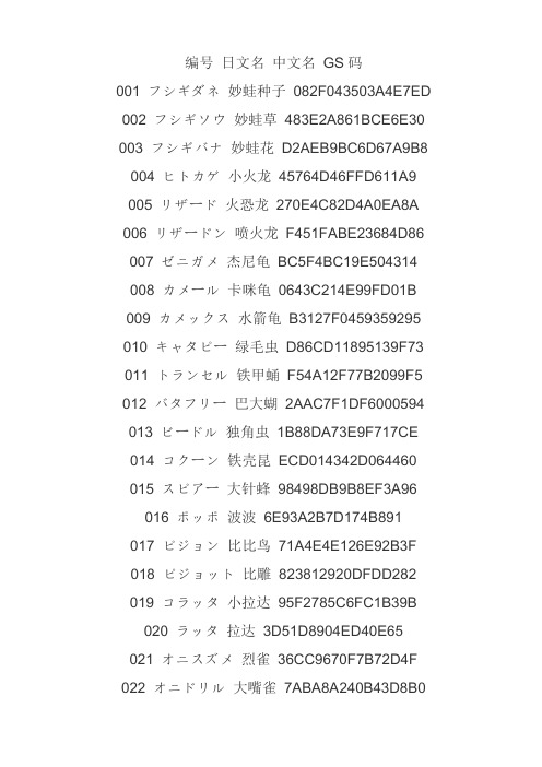
编号日文名中文名GS码001 フシギダネ妙蛙种子082F043503A4E7ED 002 フシギソウ妙蛙草483E2A861BCE6E30 003 フシギバナ妙蛙花D2AEB9BC6D67A9B8 004 ヒトカゲ小火龙45764D46FFD611A9 005 リザード火恐龙270E4C82D4A0EA8A 006 リザードン喷火龙F451FABE23684D86 007 ゼニガメ杰尼龟BC5F4BC19E504314 008 カメール卡咪龟0643C214E99FD01B 009 カメックス水箭龟B3127F0459359295 010 キャタピー绿毛虫D86CD11895139F73 011 トランセル铁甲蛹F54A12F77B2099F5 012 バタフリー巴大蝴2AAC7F1DF6000594 013 ビードル独角虫1B88DA73E9F717CE 014 コクーン铁壳昆ECD014342D064460 015 スピアー大针蜂98498DB9B8EF3A96016 ポッポ波波6E93A2B7D174B891 017 ピジョン比比鸟71A4E4E126E92B3F 018 ピジョット比雕823812920DFDD282 019 コラッタ小拉达95F2785C6FC1B39B020 ラッタ拉达3D51D8904ED40E65 021 オニスズメ烈雀36CC9670F7B72D4F 022 オニドリル大嘴雀7ABA8A240B43D8B0023 アーボ阿柏蛇4E8EC670690E8BA5 024 アーボック阿柏怪F51E51FA6577292C 025 ピカチュウ皮卡丘ED186531EE2DC737 026 ライチュウ雷丘70AEB016B7A46A34027 サンド穿山鼠4F27932231109752 028 サンドパン穿山王92676644500CFFBD 029 ニドラン♀ 尼多兰803D970B3C4D48FF 030 ニドリーナ尼多娜B3B4E37E5A0953B4 031 ニドクイン尼多后CAE6B5418DBF002B 032 ニドラン♂ 尼多朗7CED4776C9BC5FFF 033 ニドリーノ尼多利诺637E912A7D26948D 034 ニドキング尼多王C91A7E975E30F8F1 035 ピッピ皮皮0C29B3E6E87A80D7 036 ピクシー皮可西D6069AA6B178F47E037 ロコン六尾DF5136F259619CCA 038 キュウコン九尾DB9E0DD4DC880795 039 プリン胖丁54AAF8399CFE3578 040 プクリン胖可丁D2EDF2A4682C6E04 041 ズバット超音蝠BD503F7F0F3B6CCC 042 ゴルバット大嘴蝠3D6CA3B47B8DC92B 043 ナゾノクサ走路草4E2667A2888B1ADE 044 クサイハナ臭臭花EB3DEB5E8F3F0762 045 ラフレシア霸王花78D94F49A59AD633046 パラス派拉斯9FC73DD37A6857E3 047 パラセクト派拉斯特CB5FEB78A1832458 048 コンパン毛球0C53A30CB3B74FA1 049 モルフォン末入蛾D0AC0DDF28E2C76A 050 ディグダ地鼠3A9AA0A39F036981 051 ダグトリオ三地鼠E3E97E4907793FD1 052 ニャース喵喵0128F01179EA209C 053 ペルシアン猫老大DF7EC698E086864B 054 コダック可达鸭2BC83B45A68BFDE5 055 ゴルダック哥达鸭66641EA91F326429056 マンキー猴怪087074EC24E5C796 057 オコリザル火爆猴53E68CBEA3AED5B7 058 ガーディ卡蒂狗DA853A26ED454B3E 059 ウインディ风速狗5250ED1E7BFACDDE 060 ニョロモ蚊香蝌蚪A94A3E55C8A239EA 061 ニョロゾ蚊香蛙6FD99E1996B6B086 062 ニョロボン快泳蛙67E8B7645554B888 063 ケーシィ凯西E7450B71C498B8B9 064 ユンゲラー勇吉拉1F33E3D39805522B 065 フーディン胡地3D6614CAEB74A686 066 ワンリキー腕力0FFD43DF66E662C0 067 ゴーリキー豪力47D305AF7342D668 068 カイリキー怪力F62201DA0E9508BB069 マダツボミ喇叭芽186FA2C634DD0F8D070 ウツドン口呆花2DF82722F7DA5123071 ウツボット大食花96DE266F2184512A 072 メノクラゲ玛瑙水母22F15FD590E8F0BD 073 ドククラゲ毒刺水母04D90CDFC05A5514 074 イシツブテ小拳石0AA34327D6893732075 ゴローン隆隆石610329D74685888F076 ゴローニャ隆隆岩9BBA394BF03F9C85077 ポニータ小火马5F5000BA70E22EDA078 ギャロップ烈焰马C1F6A71D4D836334079 ヤドン呆呆兽81051F88DDEA905D080 ヤドラン呆河马EDF4DEB6A1CD3B43081 コイル小磁怪72C47D7FDA7497A8082 レアコイル三合一磁怪DEFBD36BEB91B231 083 カモネギ大葱鸭5274B2331C3AB5A9084 ドードー嘟嘟82E21AC20E5C5323085 ドードリオ嘟嘟利5A12018B1DBAE403086 パウワウ小海狮ECC827399FF61ED1087 ジュゴン白海狮8130BAEBD40F9B20088 ベトベター臭泥33FC175C38273B1D089 ベトベトン臭臭泥C8A3092E85ABF252 090 シェルダー大舌贝A0921CEE9B1435DF 091 パルシェン铁甲贝6E9B9A58CEA840E4092 ゴース鬼斯6F41ABE1874E212E 093 ゴースト鬼斯通CCC4429BA1AFE787094 ゲンガー耿鬼5A2C3F170F3C8E8D095 イワーク大岩蛇2CF19EE240C3A811096 スリープ素利普48F8962E040E4DD0 097 スリーパー素利柏5F68CE65571B24D7098 クラブ大钳蟹34A91C9B09D163F1 099 キングラー巨钳蟹C2FCE4DC1063A38F 100 ビリリダマ雷电球D7EDD4010B653DD6 101 マルマイン顽皮弹760D57F52D2FDECE 102 タマタマ蛋蛋534DC146108B2E58103 ナッシー椰蛋树4FD6DD8E43C42AE5 104 カラカラ可拉可拉FBE4E786112D8B22 105 ガラガラ嘎拉嘎拉4B3B9D02EE88FDF6 106 サワムラー沙瓦郎E942CCC5C5CC1B5A 107 エビワラー艾比郎8C72BA83E6ED40A1 108 ベロリンガ大舌头2BDEFE899CE3324F 109 ドガース瓦斯弹C0F811884C467FAB 110 マタドガス双弹瓦斯6DCBE85BA9FDBDB3 111 サイホーン铁甲犀牛FCEF8534EE8C31A3 112 サイドン铁甲暴龙1692A749C598C0C1 113 ラッキー吉利蛋79C0D7110F3CB283 114 モンジャラ蔓藤怪FDC8FD03BB1849E5115 ガルーラ袋龙72A6E419ACB9733F116 タッツー墨海马D34D0F32017EAC15117 シードラ海刺龙692936C6E0F03247 118 トサキント角金鱼E8BED70F5123881D 119 アズマオウ金鱼王A3C37E32F8421AAC 120 ヒトデマン海星星696000963AD8D3F6 121 スターミー宝石海星5BC4EEB96E96EFA5 122 バリヤード吸盘魔偶627452613EC2FFDE 123 ストライク飞天螳螂1EE17933164C6E7F 124 ルージュラ迷唇姐F3A9EC3C992834F6 125 エレブー电击兽F01E742CCE099315 126 ブーバー鸭嘴火龙C241F30DD8A85532 127 カイロス大甲3E597B183B3306E4 128 ケンタロス肯泰罗2E5B8430F18EE879 129 コイキング鲤鱼王99E0AA74F854F3D0 130 ギャラドス暴鲤龙DC48D07310002AE8 131 ラプラス乘龙1DE60C08620820A1132 メタモン百变怪F5F276806A896E85133 イーブイ伊布7E412C931CA2F132 134 シャワーズ水精灵C768CF5C2E57CFC4 135 サンダース雷精灵DD9AABAF6073EB75 136 ブースター火精灵39F6D058BDAC1E0F 137 ポリゴン3D龙5B0E30B7D44E55B6138 オムナイト 菊石兽 323788633ADA92C0 139 オムスター 多刺菊石兽 1EEFF7814DFC1293140 カブト 化石盔 CA61B3F1211C2582141 カブトプス 镰刀盔 51AAD0E24D35452F 142 プテラ 化石翼龙 706703EF10641042143 カビゴン 卡比兽 8A5767AF63429CB7144 フリーザー 急冻鸟 A41D0ACEFF8012A1 145 サンダー 闪电鸟 DDF12C1C65CEDB4C 146 ファイアー 火焰鸟 30E6775F95A264DE 147 ミニリュウ 迷你龙 3F9501D587B284BD 148 ハクリュー 哈克龙 4021C6C9E11E7AA9 149 カイリュー 快龙 B7B5DC94CD642A93150 ミュウツー 超梦 04213FE23BFBBB48151 ミュウ 梦幻 85D457A423876A92回复 引用举报离线高攻只看该作者 9楼 发表于: 2006-01-24152 チコリータ 菊草叶 055DF79CAEDC63E6 153 ベイリーフ 月桂叶 2858DEA02E895B发帖574帅气金钱2510在线时间0 小时注册时间2006-01-15 ∙加关注∙发消息28154 メガニウム大菊花A63AA02F660986F0155 ヒノアラシ火球鼠3B81E34E19F077AA156 マグマラシ火岩鼠7AC7F62E1680E1BE157 バクフーン火爆兽AA81FF5A264F354F158 ワニノコ小锯鳄3A24D35C5C34EFC3159 アリゲイツ蓝鳄A6E78325C594109D160 オーダイル大力鳄C03ED3C894BD6C1D161 オタチ尾立926D27E1675BF1C6 162 オオタチ大尾立9857BFC6C28A3DA7163 ホーホー咕咕7DB7CB2C21FC8D8B 164 ヨルノズク猫头夜鹰D615D168D59BA45B165 レディバ巴瓢虫FC1A579B9C7F875A166 レディアン安瓢虫BD9D2F2E3364AE3C167 イトマル线球68093FF912BF7D77 168 アリアドス阿利多斯F1AB3F439528E52B169 クロバット叉字蝠56599D12BDF50F2E170 チョンチー灯笼鱼3E8A50744277E337171 ランターン电灯怪001FDFFF21882F68172 ピチュー皮丘714D6B298BC6EC22 173 ピィ皮宝宝1F35494A1DCE6EDE 174 ププリン宝宝丁68CE86AFDDB75669175 トゲピー波克比9BE04CB6EB4A9965176 トゲチック波克基古AE05D51F3C251E59177 ネイティ天然雀0AE12087E4497B1E178 ネイティオ天然鸟A96C3FDD7387A1A8179 メリープ咩利羊BEACBE962568D1CE180 モココ绵绵05EB2EEA908D3FE5 181 デンリュウ电龙8142ACCA3E9521C9182 キレイハナ美丽花833055E891AFFAC1183 マリル玛力露A85CECECE6A8B050 184 マリルリ玛力露力0C6B34898965528E185 ウソッキー胡说树7F874B2BB9A4E769186 ニョロトノ牛蛙君3A1C188D9D317AD9187 ハネッコ毽子草D92133ABC22965D9188 ポポッコ毽子花E6E5C2C4B87E2217189 ワタッコ毽子棉3E3A1A4844B18551190 エイパム长尾怪手78E03E5BC1A6873C191 ヒマナッツ向日种子260461FCCEF855D9192 キマワリ向日花怪DE2CCF951521BDF2193 ヤンヤンマ阳阳玛B5A29AA795844206194 ウパー乌波75CE0975A57E63BC 195 ヌオー沼王DAF45ACC2DE4BE53 196 エーフィ太阳精灵26891F77B0BF1A6A197 ブラッキー月精灵5CB6CB2D968C4B64198 ヤミカラス黑暗鸦2EBA5B47D7F7C439199 ヤドキング呆兽王F7D72DA3BAFB25EE200 ムウマ梦妖5254BFFD294B828D201 アンノーンA未知图腾A723BEADF1411A322BC391B39201 アンノーンC未知图腾C94FEA989F6B4B04E201 アンノーンD未知图腾DBDC945D77111BF0E201 アンノーンE未知图腾EA572825E80AD79F2201 アンノーンF未知图腾FC2F5FA16733C7807201 アンノーンG未知图腾G8BE9D4DCA2F95FD6201 アンノーンH未知图腾H30EA5B87DCF75901201 アンノーンI未知图腾I7577BD419F62A2EC201 アンノーンJ未知图腾J3ED7A829A50633AA201 アンノーンK未知图腾K8803EF14961360E2201 アンノーンL未知图腾LD2BAC2BBB2AE1D0432B73A8201 アンノーンN未知图腾N3E420717EB0CBD15201 アンノーンO未知图腾O748C5CCD51225A39201 アンノーンP未知图腾P6220ABFC4FC2AD90201 アンノーンQ未知图腾QAA8E07719AB45062201 アンノーンR未知图腾RB25A472574A144B3201 アンノーンS未知图腾SDA6BC901AF744483201 アンノーンT未知图腾T10729C6128F2E8C8201 アンノーンU未知图腾UAEC7AE5120EF592D201 アンノーンV未知图腾V3FD87557225E8CC8201 アンノーンW未知图腾W360E89CB3B5401A380873789201 アンノーンY未知图腾Y148BF7B756890CF0201 アンノーンZ未知图腾Z8A9740A4966404F2202 ソーナンス果然翁FE7B04A31BC9CC0B203 キリンリキ麒麟奇580DB3ED8B3C2A2A204 クヌギダマ榛果球E5776A5DF552CB4D205 フォレトス佛烈托斯4A868ED3C0FCC74F206 ノコッチ土龙弟弟848FCE9AAA4AAE76207 グライガー天蝎9479CA9A0D23258E208 ハガネール大钢蛇508FA304F5375F02209 ブルー布卢EBB0073358998224 210 グランブル布卢皇E1EA29F49FD12A211 ハリーセン千针鱼EEF3D5C732A65F7F212 ハッサム巨钳螳螂8DCE3BFDC7A14ADD213 ツボツボ壶壶D61497A93D03FA5F 214 ヘラクロス赫拉克罗斯7EF393ADD62F87DC215 ニューラ狃拉4DAF280FBF15051C 216 ヒメグマ熊宝宝A1A4CE4013657A70217 リングマ圈圈熊D8DA7BAA4F588281218 マグマッグ熔岩虫05C3397946EB303E219 マグカルゴ熔岩蜗牛2AB43205FABC6FF5220 ウリムー小山猪CB0B64348D12FC36221 イノムー长毛猪54F6DC63EA15CACD222 サニーゴ太阳珊瑚11E07E0899B3CB223 テッポウオ铁炮鱼E8BA3E38409543FB224 オクタン章鱼桶C1DEAC4C64D851A5225 デリバード信使鸟B90C6ECB6BC2229B226 マンタイン巨翅飞鱼B3FFB0A666823D98227 エアームド盔甲鸟668AD40AE7BA8E4E228 デルビル戴鲁比53545F05FCDBBE8F229 ヘルガー黑鲁加0BCB0303DFF91E2D230 キングドラ刺龙王28E8D73C14B7B12F231 ゴマゾウ小小象FB7D5413967AA153 232 ドンファン顿甲6834E032DC77BB07 233 ポリゴン3D龙2 7A4E73E665C95482234 オドシシ惊角鹿68E60EAA3A91D7D3235 ドーブル图图犬1AFD8F3F08D85085236 バルキー巴尔郎61292A76CFD22B51237 カポエラー柯波朗40D79A22365A2A6D238 ムチュール迷唇娃BDEB47F4CB5EB6B8239 エレキッド电击怪399BABA7E2C0B2CD240 ブビィ小鸭嘴龙5E2FE0CC1A3120F4241 ミルタンク大奶罐9623903001C7BF60242 ハピナス幸福蛋CF930C385D5C75B6243 ライコウ雷公5782AA1383518AAC 244 エンテイ炎帝11BF55279E0ED4DA 245 スイクン水君BA3A82D5992149F4246 ヨーギラス由基拉E8747E3B65B231BA247 サナギラス沙基拉223B12243790D12E248 バンギラス班吉拉E6601D6D74A2F234249 ルギア洛奇亚B2417B603CEE43EC250 ホウオウ凤王17FF9CD47344A847251 セレビィ雪拉比A8FBA16EE5D92BC9回复引用举报离线高攻发帖574帅气只看该作者10楼发表于: 2006-01-24252 キモリ木守宫26FD6C0632F789E2253 ジュプトル森林蜥蜴7A30CB39018FD4EA254 ジュカイン蜥蜴王A086978C56076E69255 アチャモ火稚鸡AA0D5A4DD866D8DC金钱2510在线时间0 小时注册时间2006-01-15 ∙加关注∙发消息256 ワカシャモ力壮鸡574C1447BAD9D091257 バシャーモ火焰鸡08D073D31845BB05258 ミズゴロウ水跃鱼9DA259E119D91BCB259 ヌマクロー沼跃鱼8F063467E95EB6C5260 ラグラージ巨沼怪771DF2A2EF16293E261 ポチエナ土狼犬46D472F2FD7AF29C262 グラエナ大狼犬F0A7B4DF4BD58023263 ジグザグマ蛇纹熊2FC992E3212F1A17264 マッスグマ直冲熊3D705B62D7BC2FE0265 ケムッソ刺尾虫E796A028160AC07A266 カラサリス甲壳蛹C5F8FB45912FB5E9267 アゲハント狩猎凤蝶7E36341168F145D2268 マユルド盾甲茧C20A3807EF87AEA9269 ドクケイル毒粉蝶9E51BC0905A70261270 ハスボー莲叶童子B9C1BBB6FC720D8E271 ハスブレロ莲帽小童72B08A86061F7247272 ルンパッパ乐天河童E3A8FF7A55F168F6273 タネボー橡实果80DC79ABA6FC982C274 コノハナ长鼻叶B9ECD4DE32274ED3275 ダーテング狡猾天狗B92267207C9DB79F276 スバメ傲骨燕2B138A8666A36DEB 277 オオスバメ大王燕EEC121B6D9E1CC86278 キャモメ长翅鸥4FFE8E5A4450DAD279 ペリッパー大嘴鸥52B599F1D1730F71280 ラルトス拉鲁拉丝C23FD73A6C977E2E281 キルリア奇鲁莉安C503D6CF1414E015282 サーナイト沙奈朵DFA08776ABC77D44283 アメタマ雨蜘蛛C5838824C3885063284 アメモース雨翅蛾D8F1E0CDE359D5C5285 キノココ磨磨菇60996B96A203569C286 キノガッサ斗笠菇9040A99679E6CEB6287 ナマケロ懒人翁AD4DA1C69451E147288 ヤルキモノ过动猿3E4A6A0FCCDCF540289 ケッキング请假王CB75FF1D988594290 ツチニン土居忍士B4D9965E26D5FD3A291 テッカニン铁面忍者5C24C4544A14508A292 ヌケニン脱壳忍者E43838C9FC287259293 ゴニョニョ咕妞妞CC5895290250BC7E294 ドゴーム吼爆弹33AF2A790B7A8BDD295 バクオング爆音怪283029C7C68F3D07296 マクノシタ幕下力士24A5637EAB3BF86D297 ハリテヤマ超力王31B7B6EE0290C737298 ルリリ露利丽D9803312F502DF8D 299 ノズパス朝北鼻42E789203A4CC1B8300 エネコ向尾猫693A69EAC572F8EA301 エネコロロ优雅猫270D2F7D2524368E302 ヤミラミ勾魂眼17BEE25B0BAF9EB3303 クチート大嘴娃375CBB328FDB2217304 ココドラ可可多拉3BF239B00019AAD9305 コドラ可多拉59A68CFB65F0BE22 306 ボスゴドラ波士可多拉685A3CADB553EF33307 アサナン玛沙那1626A176D978292A308 チャーレム恰雷姆704F7DE89DFDAF18309 ラクライ落雷兽C4F99429CDBCA392310 ライボルト雷电兽2B6DED426397C1D2311 プラスル正电拍拍628EAB797167F1FA312 マイナン负电拍拍C5866EFD33783CBE313 バルビート电萤虫6D2D1306397C5C2E314 イルミーゼ甜甜萤008434132111FC29315 ロゼリア毒蔷薇D6247FACFB65D6EA316 ゴクリン溶食兽4EBCAA0A1739F6CE317 マルノーム吞食兽0E08514FB8739319318 キバニア利牙鱼18B8746A036C1E6D319 サメハダー巨牙鲨4022750CE8F057F8320 ホエルコ吼吼鲸84D9EBBCB663719B321 ホエルオー吼鲸王050A99F54D51AA4B322 ドンメル呆火驼CEDF2BF4CA1DB13C323 バクーダ喷火驼BAD607A4F5891F69324 コータス煤炭龟FD359CFA2A24CE91325 バネブー跳跳猪C959D2A1629D413B326 ブーピッグ噗噗猪79C9C5F2FDA6A748327 パッチール晃晃斑5B7DA1A1D117AE31328 ナックラー大颚蚁E6C80ACC795BCAEF329 ビブラーバ超音波幼虫DE135D22C45E8387330 フライゴン沙漠蜻蜓DF2A0FD888BC2E75331 サボネア沙漠奈亚18251670BA16FB6D332 ノクタス梦歌奈亚0E2CCE670DA344A5333 チルット青绵鸟5472CAC94650012E 334 チルタリス七夕青鸟5DAB14D1B537335 ザングース猫鼬斩C4DA6D6231AD75FC336 ハブネーク饭匙蛇96627B82DF65071D337 ルナトーン月亮岩0EDB8C7D021998D5338 ソルロック太阳岩DB6AA0B3D431B769339 ドジョッチ泥泥鳅A03665B7013FBFE8340 ナマズン鲶鱼王45C4744BE9031995341 ヘイガニ龙虾小兵9CAFBE2B769A21D1342 シザリガー铁蛰龙虾60A42196D054DFF5343 ヤジロン天秤偶405B381FDBD9C36F344 ネンドール念力土偶F64C71EAA2B7530D345 リリーラ触手百合BC7D76FB55C42346 ユレイドル摇篮百合887043A8B8EC4946347 アノプス太古羽虫92E64A19C1BD729E348 アーマルド太古盔甲718599796E681E92349 ヒンバス笨笨鱼44BC0D8B9AD3088A350 ミロカロス美纳斯44E29572FBE304B1351 ポワルンN天气小子-NF908E2B3C7F3701E351 ポワルン雪天气小子-雪AD18A7F5C2E2C4DA351 ポワルン晴天气小子-晴39DDA991C0DF7F2C351 ポワルン雨天气小子-雨106ADA657A3A588A352 カクレオン变隐龙79147956EB198A93353 カゲボウズ怨影娃娃B23B4138EE9A354 ジュペッタ诅咒娃娃6E2E71321DB15A51355 ヨマワル夜骷颅AF58E2CDB653E103356 サマヨール夜巨人8E1AF731F0EBC2EF357 トロピウス热带龙B2BA7076E0EECAAD358 チリーン风铃铃4DE969C7F9DC2D44359 アブソル阿勃梭鲁ED9357EC6FE8BFFE360 ソーナノ小果然翁76DA159FDC0A8624361 ユキワラシ雪童子E0A25F6EFA55310F362 オニゴーリ冰鬼护747C81BB12DACA11363 タマザラシ海豹球AB8FE43FDC5FEB2D364 トドグラー海魔狮199214359B61ADC0365 トドゼルガ帝牙海狮0BBAF430E8C01FD6366 パールル珍珠贝D625EFD8DF530001367 ハンテール猎斑鱼5EAE2E7AC4F14B22368 サクラビス樱花鱼FC7B272674C4DE3E369 ジーランス古空棘鱼CD40F306CF518736370 ラブカス爱心鱼B3007792C81144E6 371 タツベイ宝贝龙FA1C246CB983F569 372 コモルー甲壳龙8C163D6987E2D49E373 ボーマンダ暴蝾螈060E1B5A7CEE0C60374 ダンバル铁哑铃35FCC7F4ECFCFCF5375 メタング金属怪0ED95265094CC839376 メタグロス巨金怪B806EAEC97888965377 レジロック岩神柱E2DC36AE689E7303378 レジアイス冰神柱754FF88E0D2EF9CC379 レジスチル钢神柱BAC6AB87BC0FB157380 ラティアス拉帝亚斯6962C2C7745159D0381 ラティオス拉帝欧斯B3548E6E7AF634A8382 カイオーガ海皇牙7AA6D8B631408F4C383 グラードン古拉顿156740D3616812C8384 レックウザ裂空座12F6790F8F516F07385 ジラーチ吉拉祈E1EDAFC3FA066DCE386 デオキシスN迪欧西斯-NA7A2484E732D7FF7201 アンノーン!未知图腾!193150295AC4B710201 アンノーン?未知图腾?9790B4D865BFB479386 デオキシスA迪欧西斯-A3F27B08DF76A8786386 デオキシスD迪欧西斯-D7444B05CFD75DF60386 デオキシスS迪欧西斯-SFCEC686558F4DDE9。
颜色名称颜色对照表
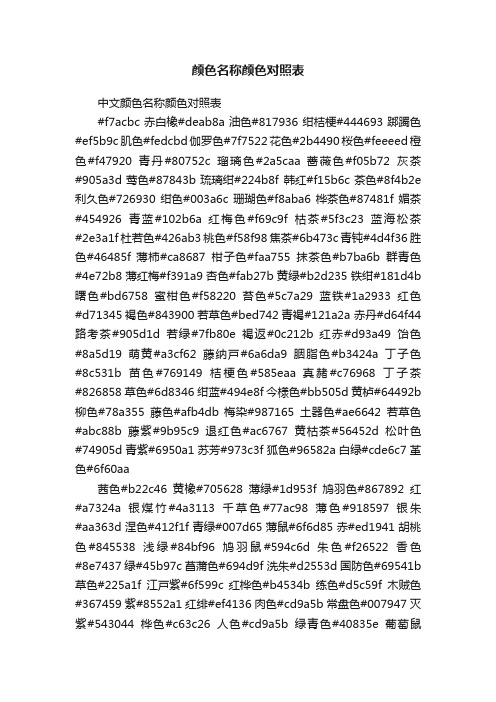
颜色名称颜色对照表中文颜色名称颜色对照表#f7acbc赤白橡#deab8a油色#817936绀桔梗#444693踯躅色#ef5b9c肌色#fedcbd伽罗色#7f7522花色#2b4490桜色#feeeed橙色#f47920青丹#80752c瑠璃色#2a5caa 蔷薇色#f05b72灰茶#905a3d莺色#87843b琉璃绀#224b8f 韩红#f15b6c茶色#8f4b2e 利久色#726930绀色#003a6c 珊瑚色#f8aba6桦茶色#87481f媚茶#454926青蓝#102b6a 红梅色#f69c9f枯茶#5f3c23蓝海松茶#2e3a1f杜若色#426ab3桃色#f58f98焦茶#6b473c青钝#4d4f36胜色#46485f 薄柿#ca8687柑子色#faa755抹茶色#b7ba6b群青色#4e72b8薄红梅#f391a9杏色#fab27b黄绿#b2d235铁绀#181d4b 曙色#bd6758蜜柑色#f58220苔色#5c7a29蓝铁#1a2933红色#d71345褐色#843900若草色#bed742青褐#121a2a 赤丹#d64f44路考茶#905d1d若绿#7fb80e褐返#0c212b 红赤#d93a49饴色#8a5d19萌黄#a3cf62藤纳戸#6a6da9胭脂色#b3424a丁子色#8c531b苗色#769149桔梗色#585eaa 真赭#c76968丁子茶#826858草色#6d8346绀蓝#494e8f 今様色#bb505d黄栌#64492b 柳色#78a355藤色#afb4db 梅染#987165土器色#ae6642若草色#abc88b藤紫#9b95c9退红色#ac6767黄枯茶#56452d松叶色#74905d青紫#6950a1苏芳#973c3f狐色#96582a白绿#cde6c7堇色#6f60aa茜色#b22c46黄橡#705628薄绿#1d953f鸠羽色#867892红#a7324a银煤竹#4a3113千草色#77ac98薄色#918597银朱#aa363d涅色#412f1f青绿#007d65薄鼠#6f6d85赤#ed1941胡桃色#845538浅绿#84bf96鸠羽鼠#594c6d 朱色#f26522香色#8e7437绿#45b97c菖蒲色#694d9f 洗朱#d2553d国防色#69541b 草色#225a1f江戸紫#6f599c 红桦色#b4534b练色#d5c59f木贼色#367459紫#8552a1红绯#ef4136肉色#cd9a5b常盘色#007947灭紫#543044桦色#c63c26人色#cd9a5b绿青色#40835e葡萄鼠#63434f 铅丹色#f3715c土色#b36d41千歳绿#2b6447古代紫#7d5886赭#a7573b小麦色#df9464深绿#005831暗红#401c44绯色#aa2116琥珀色#b76f40萌葱色#006c54葡萄#472d56丹#b64533木兰色#ad8b3d青白橡#375830茄子绀#45224a 土#b54334栀子色#dea32c革色#274d3d紫绀#411445焦香#853f04朽叶#d1923f麹尘#375830浓色#4b2f3d 真红#840228萱草色#c88400仙斎茶#27342b二蓝#402e4c 绯#7a1723黄金#c37e00若竹色#65c294菖蒲色#c77eb5红海老茶#a03939金色#c37e00青磁色#73b9a2牡丹色#ea66a6浅苏芳#8a2e3b金茶#e0861a青竹色#72baa7赤紫#f173ac 鸢色#8e453f卵色#ffce7b铁色#005344白#fffffb小豆色#8f4b4a山吹色#fcaf17锖鼠#122e29胡粉色#fffef9弁柄色#892f1b黄土色#ba8448铁御纳戸#293047生成色#f6f5ec 栗梅#6b2c25朽叶色#896a45青绿#00ae9d灰白#d9d6c3空五倍子色海老茶#733a31锖浅葱#508a88石竹色#d1c7b7#76624c深绯#54211d莺茶#6d5826水浅葱#70a19f象牙色#f2eada 赤铜色#78331e向日葵色#ffc20e新桥色#50b7c1乳白色#d3d7d4赤褐色#53261f郁金色#fdb933浅葱色#00a6ac薄钝#999d9c 金赤#f15a22砂色#d3c6a6白群#78cdd1银鼠#a1a3a6赤茶#b4533c芥子色#c7a252御纳戸色#008792茶鼠#9d9087赤锖色#84331f淡黄#dec674瓮覗#94d6da鼠色#8a8c8e 黄丹#f47a55亜麻色#b69968水色#afdfe4薄墨色#74787c 赤橙#f15a22枯色#c1a173蓝鼠#5e7c85利休鼠#7c8577柿色#f3704b鸟子色#dbce8f秘色#76becc 铅色#72777b 肉桂色#da765b黄色#ffd400空色#90d7ec灰色#77787b 桦色#c85d44蒲公英色#ffd400青#009ad6钝色#4f5555炼瓦色#ae5039中黄#ffe600蓝色#145b7d煤竹色#6c4c49锖色#6a3427刈安色#f0dc70浓蓝#11264f黒茶#563624桧皮色#8f4b38黄檗色#fcf16e勿忘草色#7bbfea黒橡#3e4145栗色#8e3e1f绿黄色#decb00露草色#33a3dc浓鼠#3c3645黄赤#f36c21鶸色#cbc547缥色#228fbd墨#464547代赭#b4532a海松色#6e6b41浅缥#2468a2黒#130c0e 骆驼色#b7704f鶸茶#596032薄缥#2570a1黒铁#281f1d 黄茶#de773f山鸠色#525f42薄花色#2585a6蝋色#2f271d洗柿#c99979生壁色#5f5d46绀青#1b315e紫黒英文颜色名称颜色对照表red green blue magenta yellow chocolate black aquamarine lime fuchsia brass azure brown bronze deeppink aliceblue gray copper coral feldspar orange orchid pink plumquartz purple aliceblueantiquewith blanchedalmondbluevioletbeige burlywood bisque cadetblue pinksaddlebrown royalblue rosybrown purple orengered olivedrabpowderbluepeachpuff papayawhippaleturquoise palevioletredpalegreen navybluenavajowhitepalegodenrod violetredyellowgreentomato turquoisethistle springgreen steelblue salmon scarlet sienna silver tan thistle turquoise violet snow salmon scarlet sienna silver tan thistle turquoise violet chartreuse firebrick gold khaki mediumslatebl mediumviole oldlace maroom goldenrod wheat ue tredwhitesmoke orange moccasin mistyrose mintcreammidnightblue dimgray darksalmon slategray skyblue sienna seashell salmon seagreensandybrownfirebrick gold khakimaroom goldenrod wheatwhitesmoke mediumturquoisenavymediumspringgreen mediumseagreenmediumpurpulperu mediumorchidmediumbluemediumaquamarinemaroon limegreen lightyellow lightsteelblue magentalightslateblue lightslategraylightskyblue inen lightseagreenlightsalmonlightpink plum lightgray lightgreenlightgodenrodyellowindianredlavender lightbluelavenderblush lightcoral lightcyanlightgodenrodhotpink greenyellowlemonchiffon lawngreen khakideepskybluehoneydew golenrod forestgreen gostwhite greenyellow gainsborofirebrick dodgerbluedarkturquoise darkslatebluedarkslategraydarkseagreendarkred darkorchid darkorengedarkslatebluedarkviolet floralwhitecyanbisquedarkgray cornsilkdarkolivegreendarkgoldenrod darkbluedarkcyan darkgreen darkhaki ivory darkmagenta darkgray cornfloewrbluecornfloewrbluedarkviolet floralwhite待补待补darkslategray darkseagreen darkred darkorchid darkorengedarkslateblueCYMK色与RGB色对照色系表CMYK四色用于出版印刷,RGB三色可用于网页制作,“#”栏中为16进制值。
AD5422中文资料
Single Channel, 16-Bit, Serial Input,Current Source & Voltage Output DAC Preliminary Technical Data AD5422Rev. PrEInformation furnished by Analog Devices is believed to be accurate and reliable. However, noresponsibility is assumed by Analog Devices for its use, nor for any infringements of patents or other rights of third parties that may result from its use. Specifications subject to change without notice. No license is granted by implication or otherwise under any patent or patent rights of Analog Devices. T rademarks and registered trademarks are the property of their respective owners. One Technology Way, P.O. Box 9106, Norwood, M A 02062-9106, U.S.A. Tel: 781.329.4700 Fax: 781.461.3113 ©2007 Analog Devices, Inc. All rights reserved.FEATURES16-Bit Resolution and MonotonicityCurrent Output Ranges: 4–20mA, 0–20mA or 0–24mA 0.1% typ Total Unadjusted Error (TUE)5ppm/°C Output DriftVoltage Output Ranges: 0-5V, 0-10V, ±5V, ±10V,10% over-range0.05% Total Unadjusted Error (TUE)3ppm/°C Output DriftFlexible Serial Digital InterfaceOn-Chip Output Fault DetectionOn-Chip Reference (10 ppm/°C Max)Asynchronous CLEAR FunctionPower Supply RangeAV DD : 10.8V to 40 VAV SS : -26.4V to -3V/0VOutput Loop Compliance to AV DD – 2.5 V Temperature Range: -40°C to +85°CTSSOP and LFCSP PackagesAPPLICATIONSProcess ControlActuator ControlPLC GENERAL DESCRIPTIONThe AD5422 is a low-cost, precision, fully integrated 16-bit converter offering a programmable current source and programmable voltage output designed to meet the requirements of industrial process control applications.The output current range is programmable to 4mA to 20 mA,0mA to 20mA or an overrange function of 0mA to 24mA. Voltage output is provided from a separate pin that can be configured to provide 0V to 5V, 0V to 10V, ±5V or ±10V output ranges, an over-range of 10% is available on all ranges. Analog outputs are short and open circuit protected and can drive capacitive loads of 1uF and inductive loads of 1H.The device is specified to operate with a power supply range from 10.8 V to 40 V. Output loop compliance is 0 V to AV DD – 2.5 V.The flexible serial interface is SPI and MICROWIRE compatible and can be operated in 3-wire mode to minimize the digital isolation required in isolated applications.The device also includes a power-on-reset function ensuring that the device powers up in a known state and an asynchronous CLEAR pin which sets the outputs to zero-scale / mid-scale voltage output or the low end of the selected current range.The total output error is typically ±0.1% in current mode and ±0.05% in voltage mode.Table 1. Related DevicesPart Number DescriptionAD5412 Single Channel, 12-Bit, SerialInput Current Source andVoltage Output DACAD5420 Single Channel, 16-Bit, SerialInput Current Source DACAD5410 Single Channel, 12-Bit, SerialInput Current Source DACAD5422Preliminary Technical DataRev. PrE | Page 2 of 37TABLE OF CONTENTSFeatures..............................................................................................1 Applications.......................................................................................1 General Description.........................................................................1 Revision History...............................................................................2 Functional Block Diagram..............................................................3 Specifications.....................................................................................4 AC Performance Characteristics................................................7 Timing Characteristics................................................................8 Absolute Maximum Ratings..........................................................10 ESD Caution................................................................................10 Pin Configuration and Function Descriptions...........................11 Typical Performance Characteristics Voltage output ...............13 Typical Performance Characteristics current output ...............17 Typical Performance Characteristics general ............................20 Terminology....................................................................................22 Theory of Operation......................................................................24 Architecture.................................................................................24 Serial Interface............................................................................24 Default configuration.................................................................28 Transfer Function.......................................................................28 Data Register...............................................................................29 Control Register..........................................................................29 RESET register............................................................................29 Status register..............................................................................30 Features............................................................................................31 fault alert......................................................................................31 voltage output short circuit protection....................................31 Asynchronous Clear (CLEAR).................................................31 Internal Reference......................................................................31 External current setting resistor...............................................31 Voltage ouTput over-range........................................................31 Digital Power Supply..................................................................31 External boost function.............................................................31 digital Slew rate control.............................................................32 I OUT Filtering Capacitors............................................................32 Applications Information..............................................................33 driving inductive loads..............................................................33 Transient voltage protection.....................................................33 Layout Guidelines.......................................................................33 Galvanically Isolated Interface.................................................33 Microprocessor Interfacing.......................................................33 Thermal and supply considerations.........................................34 Outline Dimensions.......................................................................35 Ordering Guide.. (35)REVISION HISTORYPrE – Preliminary Version, November 22, 2007Preliminary Technical DataAD5422Rev. PrE | Page 3 of 37FUNCTIONAL BLOCK DIAGRAMV OUT I OUT LATCH SCLK SDIN SDOCCAGND CLEAR FAULT BOOSTREFOUT REFIN SENSESENSECLEAR SELECT R SET DV CC C COMP2C COMP1DGND**LFCSP PackageFigure 1.AD5422Preliminary Technical DataRev. PrE | Page 4 of 37SPECIFICATIONSAV DD = 10.8V to 40V , AV SS = -26.4V to -3V/0V , AV DD + |AV SS | < 52.8V , AGND = DGND = 0 V , REFIN= +5 V external; DV CC = 2.7 V to 5.5 V , V OUT : R L = 2 kΩ, C L = 200 pF, I OUT : R L = 300Ω, H L = 50mH; all specifications T MIN to T MAX , ±10 V / 0 to 24 mA range unless otherwise noted. Table 2.Parameter Value 1 Unit Test Conditions/CommentsVOLTAGE OUTPUTOutput Voltage Ranges 0 to 5 V 0 to 10 V -5 to +5 V -10 to +10 V ACCURACY Output unloaded Bipolar Output Resolution 16 Bits Total Unadjusted Error (TUE) 0.1 % FSR max Over temperature, supplies, and time, typically 0.05%FSRTUE TC 2 ±3 ppm typ Relative Accuracy (INL) ±0.012 % FSR max Differential Nonlinearity (DNL) ±1 LSB max Guaranteed monotonic Bipolar Zero Error ±5 mV max @ 25°C, error at other temperatures obtained usingbipolar zero TCBipolar Zero TC 2±3 ppm FSR/°C max Zero-Scale Error ±1 mV max @ 25°C, error at other temperatures obtained using zeroscale TCZero-Scale TC 2±3 ppm FSR/°C max Gain Error ±0.05 % FSR max @ 25°C, error at other temperatures obtained using gainTCGain TC 2 ±8 ppm FSR/°C max Full-Scale Error 0.05 % FSR max @ 25°C, error at other temperatures obtained using gainTCFull-Scale TC 2 ±3 ppm FSR/°C max Unipolar Output AV SS = 0 V Resolution 16 Bits Total Unadjusted Error (TUE) 0.1 % FSR max Over temperature, supplies, and time, typically 0.05%FSRRelative Accuracy (INL) ±0.012 % FSR max Differential Nonlinearity (DNL) ±1 LSB max Guaranteed monotonic (at 16 bit-resolution) Zero Scale Error +10 mV max @ 25°C, error at other temperatures obtained using gainTCZero Scale TC 2±3 ppm FSR/°C max Offset Error ±10 mV max Gain Error ±0.05 % FSR max @ 25°C, error at other temperatures obtained using gainTCGain TC 2±3 ppm FSR/°C max Full-Scale Error 0.05 % FSR max @ 25°C, error at other temperatures obtained using gainTCFull-Scale TC 2±3 ppm FSR/°C maxOUTPUT CHARACTERISTICS 2eadroom 0.8 V max 0.5 V typ Output Voltage TC ±3 ppm FSR/°C max Output Voltage Drift vs. Time ±12 ppm FSR/500 hr typ Vout = ¾ of Full-Scale ±15 ppm FSR/1000 hr typ Short-Circuit Current 12 mA typPreliminary Technical DataAD5422Rev. PrE | Page 5 of 37Parameter Value 1 Unit Test Conditions/Comments Load 2 kΩ min For specified performance Capacitive Load Stability R L = ∞ 20 nF max R L = 2 kΩ TBD nF max R L = ∞ 1 µF max External compensation capacitor of 4nF connected. DC Output Impedance 0.3 Ω typ Power-On Time 10 µs typ DC PSRR TBD µV/VCURRENT OUTPUTOutput Current Ranges 0 to 24 mA 0 to 20 mA 4 to 20 mA ACCURACY Resolution 16 Bits Total Unadjusted Error (TUE) ±0.3 % FSR max Over temperature, supplies, and time, typically 0.1% FSR TUE TC 2 ±5 ppm/°C typ Relative Accuracy (INL) ±0.012 % FSR max Differential Nonlinearity (DNL) ±1 LSB max Guaranteed monotonic Offset Error ±0.05 % FSR max Offset Error Drift ±5 µv/°C typ Gain Error ±0.02 % FSR max @ 25°C, error at other temperatures obtained using gainTCGain TC 2 ±8 ppm FSR/°C max Full-Scale Error 0.05 % FSR max @ 25°C, error at other temperatures obtained using gainTCFull-Scale TC 2 ±8 ppm FSR/°COUTPUT CHARACTERISTICS 2Current Loop Compliance Voltage AVDD - 2.5 V max Output Current Drift vs. Time TBD ppm FSR/500 hr typ TBD ppm FSR/1000 hr typ Resistive Load TBD Ω max Inductive Load 1 H max DC PSRR 10 µA/V max Output Impedance 50 MΩ typREFERENCE INPUT/OUTPUTReference Input 2 Reference Input Voltage 5 V nom ±1% for specified performance DC Input Impedance 30 kΩ min Typically 40 kΩ Reference Range 4 to 5 V min to V max Reference Output Output Voltage 4.998 to 5.002 V min to V max @ 25°C Reference TC ±10 ppm/°C max Output Noise (0.1 Hz to 10 Hz)2 18 µV p-p typNoise Spectral Density 2120 nV/√Hz typ @ 10 kHz Output Voltage Drift vs. Time 2 ±40 ppm/500 hr typ ±50 ppm/1000 hr typ Capacitive Load TBD nF max Load Current 5 mA typ Short Circuit Current 7 mA typ Line Regulation 2 10 ppm/V typLoad Regulation 2TBD ppm/mA Thermal Hysteresis 2 TBD ppmAD5422 Preliminary Technical Data1 Temperature range: -40°C to +85°C; typical at +25°C.2 Guaranteed by characterization. Not production tested.Rev. PrE | Page 6 of 37Preliminary Technical DataAD5422Rev. PrE | Page 7 of 37AC PERFORMANCE CHARACTERISTICSAV DD = 10.8V to 40V , AV SS = -26.4V to -3V/0V , AV DD + |AV SS | < 52.8V , AGND = DGND = 0 V , REFIN= +5 V external; DV CC = 2.7 V to 5.5 V , V OUT : R L = 2 kΩ, C L = 200 pF, I OUT : R L = 300Ω, H L = 50mH; all specifications T MIN to T MAX , ±10 V / 0 to 24 mA range unless otherwise noted. Table 3.Parameter 1 Unit Test Conditions/Comments DYNAMIC PERFORMANCEVOLTAGE OUTPUTOutput Voltage Settling Time 8 µs typ Full-scale step (10 V) to ±0.03% FSR 10 µs max 5 µs max 512 LSB step settlingOutput Current Settling Time 10 µs max To 0.1% FSR Slew Rate 1 V/µs typ Power-On Glitch Energy 10 nV-sec typ Digital-to-Analog Glitch Energy 10 nV-sec typ Glitch Impulse Peak Amplitude 20 mV typ Digital Feedthrough 1 nV-sec typ Output Noise (0.1 Hz to 10 Hz Bandwidth) 0.1 LSB p-p typ Output Noise (100 kHz Bandwidth) 80 µV rms max 1/f Corner Frequency 1 kHz typ Output Noise Spectral Density 100 nV/√Hz typ Measured at 10 kHz AC PSRR TBD dB 200mV 50/60Hz Sinewavesuperimposed on power supply voltage.CURRENT OUTPUTOutput Current Settling Time TBD µs typ To 0.1% FSR , L = 1H TBD µs typ To 0.1% FSR , L < 1mH1Guaranteed by characterization, not production tested.AD5422Preliminary Technical DataRev. PrE | Page 8 of 37TIMING CHARACTERISTICSAV DD = 10.8V to 40V , AV SS = -26.4V to -3V/0V , AV DD + |AV SS | < 52.8V , AGND = DGND = 0 V , REFIN= +5 V external; DV CC = 2.7 V to 5.5 V , V OUT : R L = 2 kΩ, C L = 200 pF, I OUT : R L = 300Ω, H L = 50mH; all specifications T MIN to T MAX , ±10 V / 0 to 24 mA range unless otherwise noted. Table 4.Parameter 1, 2, 3 Limit at T MIN , T MAX Unit DescriptionWrite Modet 1 33 ns min SCLK cycle time t 2 13 ns min SCLK low time t 3 13 ns min SCLK high time t 4 13 ns min LATCH delay time t 5 40 ns min LATCH high time t 5 5 µs min LATCH high time (After a write to the CONTROL register) t 6 5 ns min Data setup time t 7 5 ns min Data hold time t 8 40 ns min LATCH low time t 9 20 ns min CLEAR pulsewidth t 10 5 µs max CLEAR activation timeReadback Modet 11 82 ns min SCLK cycle time t 12 33 ns min SCLK low time t 13 33 ns min SCLK high time t 14 13 ns min LATCH delay time t 15 40 ns min LATCH high time t 16 5 ns min Data setup time t 17 5 ns min Data hold time t 18 40 ns min LATCH low time t 19 40 ns max Serial output delay time (C L SDO 4 = 15pF) t 20 33 ns max LATCH rising edge to SDO tri-stateDaisychain Modet 21 82 ns min SCLK cycle time t 22 33 ns min SCLK low time t 23 33 ns min SCLK high time t 24 13 ns min LATCH delay time t 25 40 ns min LATCH high time t 26 5 ns min Data setup time t 27 5 ns min Data hold time t 28 40 ns min LATCH low time t 29 40 ns max Serial output delay time (C L SDO 4 = 15pF)1 Guaranteed by characterization. Not production tested.2All input signals are specified with t R = t F = 5 ns (10% to 90% of DV CC ) and timed from a voltage level of 1.2 V. 3See Figure 2, Figure 3, and Figure 4. 4C L SDO = Capacitive load on SDO output.Preliminary Technical DataAD5422Rev. PrE | Page 9 of 37SCLK LATCHSDINCLEAROUTPUTFigure 2. Write Mode Timing DiagramSCLKLATCHSDINSDOSELECTED REGISTER DATA CLOCKED OUTFIRST 8 BITS ARE DON’T CARE BITSFigure 3. Readback Mode Timing DiagramSCLKSDINSDOLATCHFigure 4. Daisychain Mode Timing DiagramAD5422Preliminary Technical DataRev. PrE | Page 10 of 37ABSOLUTE MAXIMUM RATINGST A = 25°C unless otherwise noted.Transient currents of up to 100 mA do not cause SCR latch-up. Table 5.Parameter Rating AV DD to AGND, DGND −0.3V to 48V AV SS to AGND, DGND +0.3 V to −48 V AV DD to AV SS -0.3V to 60V DV CC to AGND, DGND −0.3 V to +7 V Digital Inputs to AGND, DGND −0.3 V to DV CC + 0.3 V or 7 V(whichever is less)Digital Outputs to AGND, DGND −0.3 V to DV CC + 0.3 V or 7V(whichever is less)REFIN/REFOUT to AGND, DGND −0.3 V to +7 V V OUT to AGND, DGND AV SS to AV DD I OUT to AGND, DGND −0.3V to AV DD AGND to DGND -0.3V to +0.3V Operating Temperature Range Industrial −40°C to +851°C Storage Temperature Range −65°C to +150°C Junction Temperature (T J max) 125°C 24-Lead TSSOP Package θJA Thermal Impedance 42°C/W 40-Lead LFCSP Package θJA Thermal Impedance 28°C/W Power Dissipation (T J max – T A )/ θJA Lead Temperature JEDEC Industry StandardSoldering J-STD-020Stresses above those listed under Absolute Maximum Ratings may cause permanent damage to the device. This is a stress rating only; functional operation of the device at these or any other conditions above those indicated in the operationalsection of this specification is not implied. Exposure to absolute maximum rating conditions for extended periods may affect device reliability.ESD CAUTION1Power dissipated on chip must be de-rated to keep junction temperature below 125°C. Assumption is max power dissipation condition is sourcing 24mA into Ground from AV DD with a 3mA on-chip current.PIN CONFIGURATION AND FUNCTION DESCRIPTIONSAGND SDOAV SSSENSE GNDLATCH CLEAR CLEAR SELECT REFIN SELECT SCLK SDIN GND R SETOUTBOOST C COMP1REFOUT DV CC C COMP2I OUTSENSEAV DDDV CCD G N G N A V S CA V S SA V D D N CN CV S E N S EV C CNCNC DV CC SELECT V S E N S EO U TBOOST C COMP1C COMP2I OUT N R S E NC A G N CN N R E F I R E F O U CAP2CAP1Figure 5. TSSOP Pin ConfigurationFigure 6. LFCSP Pin ConfigurationTSSOP Pin No. LFCSP Pin No. Mnemonic Descriptionoutputpin.19 26 I OUT Current20 27 BOOSTOptional external transistor connection. Connecting an external transistor will reducethe power dissipated in the AD5422. Refer to the features section.N/A 28 CAP1 Connection for optional output filtering capacitor. Refer to Features section.N/A 29 CAP2 Connection for optional output filtering capacitor. Refer to Features section.21 32 V OUT Buffered Analog Output Voltage. The output amplifier is capable of directly driving a 2kΩ, 2000 pF load.22 33 +V SENSE Sense connection for the positive voltage output load connection.23 34 -V SENSE Sense connection for the negative voltage output load connection.24 36 AV DD Positive Analog Supply Pin. Voltage ranges from 10.8V to 60V.Paddle Paddle AV SS Negative Analog Supply Pin. Voltage ranges from –3 V to –24 V. This pin can beconnected to 0V if output voltage range is unipolar.TYPICAL PERFORMANCE CHARACTERISTICSVOLTAGE OUTPUTFigure 7. Integral Non Linearity Error vs DAC Code (Four Traces)Figure 8. Differential Non Linearity Error vs. DAC Code (Four Traces)Figure 9. Total Unadjusted Error vs. DAC Code (Four Traces)Figure 10. Integral Non Linearity vs. Temperature (Four Traces)Figure 11. Differential Non Linearity vs. Temperature (Four Traces)Figure 12. Integral Non Linearity vs. Supply Voltage (Four Traces)Figure 13.Differential Non Linearity Error vs. Supply Voltage (Four Traces)Figure 14. Integral Non Linearity Error vs. Reference Voltage (Four traces)Figure 15. Differential Non Linearity Error vs. Reference Voltage (Four Traces)Figure 16. Total Unadjusted Error vs.Reference Voltage (Four Traces)Figure 17. Total Unadjusted Error vs. Supply Voltage (Four Traces)Figure 18. Offset Error vs.TemperatureFigure 19. Bipolar Zero Error vs. TemperatureFigure 20. Gain Error vs. TemperatureFigure 21. Source and Sink Capability of Output AmplifierFull-Scale Code LoadedFigure 22. Source and Sink Capability of Output AmplifierZero-Scale LoadedFigure 23.Full-Scale Positive StepFigure 24. Full-Scale Negative StepFigure 25. Digital-to-Analog Glitch EnergyFigure 26. Peak-to-Peak Noise (0.1Hz to 10Hz Bandwidth)Figure 27. Peak-to-Peak Noise (100kHz Bandwidth)Figure 28. V OUT vs. Time on Power-upFigure 29. V OUT vs, Time on Output EnabledTYPICAL PERFORMANCE CHARACTERISTICS CURRENT OUTPUTFigure 30. Integral Non Linearity vs. CodeFigure 31.Differential Non Linearity vs. CodeFigure 32. Total Unadjusted Error vs. CodeFigure 33. Integral Non Linearity vs. TemperatureFigure 34. Differential Non Linearity vs. TemperatureFigure 35. Integral Non Linearity vs. SupplyFigure 36. Differential Non Linearity vs. Supply VoltageFigure 37. Integral Non Linearity vs. Reference VoltageFigure 38. Differential Non Linearity vs. Reference VoltageFigure 39. Total Unadjusted Error vs. Reference VoltageFigure 40. Total Unadjusted Error vs. Supply VoltageFigure 41. Offset Error vs. TemperatureFigure 42. Gain Error vs. TemperatureFigure 43. Voltage Compliance vs. TemperatureFigure 44. I OUT vs. Time on Power-upFigure 45. I OUT vs. Time on Output EnabledTYPICAL PERFORMANCE CHARACTERISTICS GENERALFigure 46. DI CC vs.Logic Input VoltageFigure 47. AI DD /AI SS vs AV DD /AV SSFigure 48. AI DD vs AV DDFigure 49. DVCC Output Voltage vs. DI CC Load CurrentFigure 50. Refout Turn-on TransientFigure 51. Refout Output Noise (0.1Hz to 10Hz Bandwidth)Figure 52. Refout Output Noise (100kHz Bandwidth)Figure 53. Refout Line TransientFigure 54. Refout Load TransientFigure 55. Refout Histogram of Thermal HysteresisFigure 56. Refout Voltage vs. Load CurrentTERMINOLOGYRelative Accuracy or Integral Nonlinearity (INL)For the DAC, relative accuracy, or integral nonlinearity (INL), is a measure of the maximum deviation, in LSBs, from a straight line passing through the endpoints of the DAC transfer function. A typical INL vs. code plot can be seen in Figure 7. Differential Nonlinearity (DNL)Differential nonlinearity (DNL) is the difference between the measured change and the ideal 1 LSB change between any two adjacent codes. A specified differential nonlinearity of ±1 LSB maximum ensures monotonicity. This DAC is guaranteed monotonic by design. A typical DNL vs. code plot can be seen in Figure 10.MonotonicityA DAC is monotonic if the output either increases or remains constant for increasing digital input code. The AD5724R/AD5734R/AD5754R are monotonic over their full operating temperature range.Bipolar Zero ErrorBipolar zero error is the deviation of the analog output from the ideal half-scale output of 0 V when the DAC register is loaded with 0x8000 (straight binary coding) or 0x0000 (twos complement coding). A plot of bipolar zero error vs. temperature can be seen in Table TBD.Bipolar Zero TCBipolar zero TC is a measure of the change in the bipolar zero error with a change in temperature. It is expressed in ppm FSR/°C.Full-Scale ErrorFull-Scale error is a measure of the output error when full-scale code is loaded to the DAC register. Ideally, the output should be full-scale − 1 LSB. Full-scale error is expressed in percent offull-scale range (% FSR).Negative Full-Scale Error/Zero-Scale ErrorNegative full-scale error is the error in the DAC output voltage when 0x0000 (straight binary coding) or 0x8000 (twos complement coding) is loaded to the DAC register. Ideally, the output voltage should be negative full-scale− 1 LSB. A plot of zero-scale error vs. temperature can be seen in Table TBD Zero-Scale TCThis is a measure of the change in zero-scale error with a change in temperature. Zero-scale error TC is expressed in ppm FSR/°C. Output Voltage Settling TimeOutput voltage settling time is the amount of time it takes for the output to settle to a specified level for a full-scale input change. A plot of settling time can be seen in Table TBD Slew RateThe slew rate of a device is a limitation in the rate of change of the output voltage. The output slewing speed of a voltage-output D/A converter is usually limited by the slew rate of the amplifier used at its output. Slew rate is measured from 10% to 90% of the output signal and is given in V/µs.Gain ErrorThis is a measure of the span error of the DAC. It is the deviation in slope of the DAC transfer characteristic from ideal expressed in % FSR. A plot of gain error vs. temperature can be seen in Table TBDGain TCThis is a measure of the change in gain error with changes in temperature. Gain Error TC is expressed in ppm FSR/°C. Total Unadjusted ErrorTotal unadjusted error (TUE) is a measure of the output error taking all the various errors into account, namely INL error, offset error, gain error, and output drift over supplies, temperature, and time. TUE is expressed in % FSR.Current Loop Voltage ComplianceThe maximum voltage at the I OUT pin for which the output currnet will be equal to the programmed value.Power-On Glitch EnergyPower-on glitch energy is the impulse injected into the analog output when the AD5422 is powered-on. It is specified as the area of the glitch in nV-sec. See Table TBDDigital-to-Analog Glitch ImpulseDigital-to-analog glitch impulse is the impulse injected into the analog output when the input code in the DAC register changes state, but the output voltage remains constant. It is normally specified as the area of the glitch in nV-sec and is measured when the digital input code is changed by 1 LSB at the major carry transition (0x7FFF to 0x8000). See Table TBDGlitch Impulse Peak AmplitudeGlitch impulse peak amplitude is the peak amplitude of the impulse injected into the analog output when the input code in the DAC register changes state. It is specified as the amplitude of the glitch in mV and is measured when the digital input code is changed by 1 LSB at the major carry transition (0x7FFF to0x8000). See Table TBD.Digital FeedthroughDigital feedthrough is a measure of the impulse injected into the analog output of the DAC from the digital inputs of the DAC, but is measured when the DAC output is not updated. It is specified in nV-sec and measured with a full-scale code change on the data bus.Power Supply Rejection Ratio (PSRR)PSRR indicates how the output of the DAC is affected by changes in the power supply voltage.Reference TCReference TC is a measure of the change in the reference output voltage with a change in temperature. It is expressed in ppm/°C. Line RegulationLine regulation is the change in reference output voltage due to a specified change in supply voltage. It is expressed in ppm/V. Load RegulationLoad regulation is the change in reference output voltage due to a specified change in load current. It is expressed in ppm/mA. Thermal HysteresisThermal hysteresis is the change of reference output voltage after the device is cycled through temperatures from +25°C to −40°C to +85°C and back to +25°C. This is a typical value from a sample of parts put through such a cycle. See Table TBDfor a histogram of thermal hysteresis.TCOOHYSOVVV__C)25(−°=6__10C)25(C)25()(×°−°=OTCOOHYSO VVVppmVwhere:V O(25°C) = V O at 25°CV O_TC = V O at 25°C after temperature cycleTHEORY OF OPERATIONThe AD5422 is a precision digital to current loop and voltage output converter designed to meet the requirements of industrial process control applications. It provides a high precision, fully integrated, low cost single-chip solution for generating current loop and unipolar/bipolar voltage outputs. The current ranges available are; 0 to 20mA, 0 to 24mA and 4 to 20mA, the voltage ranges available are; 0 to 5V , ±5V , 0 to 10V and ±10V , the current and voltage outputs are available onseparate pins and only one is active at any one time. The desired output configuration is user selectable via the CONTROL register.ARCHITECTUREThe DAC core architecture of the AD5422 consists of two matched DAC sections. A simplified circuit diagram is shown in Figure 57. The 4 MSBs of the 16-bit data word are decoded to drive 15 switches, E1 to E15. Each of these switches connects 1 of 15 matched resistors to either ground or the reference buffer output. The remaining 12 bits of the data-word drive switches S0 to S11 of a 12-bit voltage mode R-2R ladder network.V REFV OUT12-BIT R-2R LADDE RFOUR MSBs DECODED INTO 15 EQUAL SEGMENTSFigure 57. DAC Ladder StructureThe voltage output from the DAC core is either converted to a current (see diagram, Figure 58) which is then mirrored to the supply rail so that the application simply sees a current source output with respect to ground or it is buffered and scaled to output a software selectable unipolar or bipolar voltage range (See diagram, Figure 59). The current and voltage are output onseparate pins and cannot be output simultaneously.I OUTFigure 58. Voltage to Current conversion circuitryREFINL1Figure 59. Voltage OutputVoltage Output AmplifierThe voltage output amplifier is capable of generating both unipolar and bipolar output voltages. It is capable of driving a load of 2 kΩ in parallel with 1 µF to AGND. The source and sink capabilities of the output amplifier can be seen in Figure TBD. The slew rate is 1 V/µs with a full-scale settling time of 10 µs, (10V step). Figure 59 shows the voltage output drving a load, R L on top of a common mode voltage of up to ±3V .In output module applications where a cable could possibly become disconnected from +V SENSE resulting in the amplifier loop being broken and most probably resulting in largedestructive voltages on V OUT , a resistor, R 1, of value 2k Ω to 5k Ω should be included as shown to ensure the amplifier loop is kept closed.Driving Large Capacitive LoadsThe voltage output amplifier is capable of driving capacitive loads of up to 1uF with the addition of a non-polarised 4nF compensation capacitor between the C COMP1 and C COMP2 pins. Without the compensation capacitor, up to 20nF capacitive loads can be driven.Reference BuffersThe AD5422 can operate with either an external or internal reference. The reference input has an input range of 4 V to 5 V , 5 V for specified performance. This input voltage is then buffered before it is applied to the DAC.SERIAL INTERFACEThe AD5422 is controlled over a versatile 3-wire serial interface that operates at clock rates up to 30 MHz. It is compatible with SPI®, QSPI™, MICROWIRE™, and DSP standards.Input Shift RegisterThe input shift register is 24 bits wide. Data is loaded into the device MSB first as a 24-bit word under the control of a serial clock input, SCLK. Data is clocked in on the rising edge of SCLK. The input register consists of 8 control bits and 16 data bits as shown in Table 7. The 24 bit word is unconditionally latched on the rising edge of LATCH. Data will continue to be clocked in irrespective of the state of LATCH, on the rising edge of LATCH the data that is present in the input register will be latched, in other words the last 24 bits to be clocked in before。
AD421中文资料
这款DAC采用Σ-Δ架构,可保证16位单调性,且积分非线 性为±0.01%。该器件提供4 mA零电平输出电流(失调误差 为±0.1%),以及20 mA满量程输出电流(增益误差为±0.2%)。
单位
条件/注释
精度 分辨率 单调性 积分非线性 失调(4 mA)(+25°C时)4 失调漂移 典型输出误差(20 mA) (+25°C时)4 总输出漂移 VCC电源灵敏度
16 16 ± 0.01 ± 0.1 ± 25 ± 0.2 ± 50 50
位 位(最小值) % FS(最大值) % FS(最大值) ppm FS/°C(最大值) % FS(最大值) ppm FS/°C(最大值) nA/mV(最大值)
FS = 满量程输出电流 VCC = 5 V 包括片内基准电压漂移 VCC = 5 V 包括片内基准电压漂移 25 nA/mV(典型值)
基准电压源 REF OUT2 输出电压 温漂
外部电流 VCC电源灵敏度 输出阻抗 噪声(0.1 Hz–10 Hz) REF OUT1
输出电压 温漂
外部电流 VCC电源灵敏度 输出阻抗 噪声(0.1 Hz–10 Hz) REF IN 输入电阻
7. AD421具有可编程报警电流功能,允许发射器通过发 送超量程电流来指示传感器故障。
HART是HART通信基金会的注册商标。
Rev. C
Information furnished by Analog Devices is believed to be accurate and reliable. However, no responsibility is assumed by Analog Devices for its use, nor for any infringements of patents or other rightsofthirdpartiesthatmayresultfromitsuse.Speci cationssubjecttochangewithoutnotice.No license is granted by implication or otherwise under any patent or patent rights of Analog Devices. Trademarks and registered trademarks are the property of their respective owners.
无线红外防盗报警器的设计

1 前言随着微电子技术与网络技术的飞速进展,人们关于居住环境的平安、方便、舒适提出了愈来愈高的要求因此智能化住宅就随之显现,也随着改革开放的深切和市场经济的迅速进展、提高,城市外来流动人口的大量增加,带来了许多不平安因素,刑事案件专门是入室盗窃、抢劫居高不下,因此家庭智能平安防范系统是智能化小区建设中不可缺少的一项,而以往的做法是安装防盗门、防盗网,但普遍存在有碍美观,不符合防火要求,而且不能有效地避免犯法分子对住宅的入侵,故利用高科技的电子防盗报警系统也就应运而生。
无线红外防盗报警器的进展主若是基于传感器之上,因此有必要先谈谈红别传感器的进展状况。
而传感器技术是21世纪人们在高新技术进展方面争夺的一个制高点,各发达国家都将传感技术视为现代高新技术进展的关键。
从20世纪80年代起,日本就将传感器技术列为优先进展的高新科技之首,美国等西方国家也将此技术列为国家科技和国防技术进展的重点。
从而基于传感器技术的防盗报警系统也取得了高速进展。
不管是基于哪一种方式的无线防盗报警器,它的工作原理都是将探测到的信号,通过编码,经电路放大,输出并将报警信号通过天线发射出,再用接收电路接收信号,解码并通过操纵电路判定是不是属于异样信号,再决定是不是发送报警信号给报警电路,从而达到防盗的成效,本系统也是采纳此原理。
本系统采纳经常使用的STC89C52单片机作为系统的核心操纵部份,是一个利用红别传感器作为信号输入的操纵部份的智能报警器。
当有不明人物进过红外探头时,会有操纵信号输入单片机,进而输出扎耳报警声引发相关人员的注意,同时利用显示器来显示。
如此专门大程度上减少了搜索时刻,从而提高了时效性。
达到了信号同意灵明度高,显示反映快,报警声音响的成效。
2 整体方案设计方案比较2.1.1 方案一图方案一方框图2.1.1 方案二图方案二方框图方案论证2.3.1 收发模块的比较方案一中收发模块采纳的核心芯片是Nrf905,此芯片为32引脚芯片,工作电压在,需外接433MHz 50Ω天线。
STC12C2052AD 系列单片机器件手册 说明书

STC12C2052AD 系列单片机器件手册 --- 1个时钟/机器周期8051 ---无法解密 ---低功耗,超低价 ---高速,高可靠 ---强抗静电,强抗干扰STC12C0552,STC12C0552ADSTC12C1052,STC12C1052ADSTC12C2052,STC12C2052ADSTC12C3052, STC12C3052ADSTC12C4052, STC12C4052ADSTC12C5052, STC12C5052ADSTC12LE0552,STC12LE0552ADSTC12LE1052,STC12LE1052ADSTC12LE2052,STC12LE2052ADSTC12LE3052,STC12LE3052ADSTC12LE4052,STC12LE4052ADSTC12LE5052,STC12LE5052AD技术支援:宏晶科技(深圳) www.MCU-Memory.com support@MCU-Memory.comUpdate date: 2005-10-4 (草案,请随时注意更新)宏晶科技:专业单片机/存储器供应商 www.MCU-Memory.com STC12C2052AD系列 1T 8051单片机中文指南2领导业界革命 覆盖市场需求宏晶科技是新一代增强型8051单片机标准的制定者,致力于提供满足中国市场需求的世界级高性能单片机技术,在业内处于领先地位,销售网络覆盖全国。
在保证质量的基础上,以极低的价格和完善的服务赢得了客户的长期信赖。
目前,全力推出“1个时钟/机器周期”的单片机,全面提升8051单片机性能。
欢迎海内外厂家前来洽谈合作!新客户请直接联系深圳,以获得更好的技术支持与服务。
STC 12C2052AD系列 1T 8051 单片机RST 1 20 VCCRxD/P3.0 2 19 P1.7/SCLK/ADC7TxD/P3.1 3 18 P1.6/MISO/ADC6XTAL2 4 17 P1.5/MOSI/ADC5INT0/P3.2 6 15 P1.3/ADC3INT1/P3.3 7 14 P1.2/ADC2ECI/T0/P3.4 8 13 P1.1/ADC1PWM1/PCA1/T1/P3.5 9 12 P1.0/ADC0Gnd 10 11 P3.7/PCA0/PWM0XTAL1 5 16 P1.4/SS/ADC4DIP-20,SOP-20,(超小封装TSSOP-20定货)STC12C2052、STC12C4052不带A/D转换STC12C2052AD、STC12C4052AD带A/D转换 新客户请直接联系深圳以获得更好的技术支持和服务 欢迎海内外厂家前来洽谈合作南京办:广州办: 传真至深圳申请STC单片机 样片及ISP下载线/编程工具1个时钟/机器周期,超小封装8051单片机在系统可编程,无需编程器,可远程升级可送STC-ISP下载编程器,1万片/人/天内部集成MAX810专用复位电路,原复位电路可以保留,也可以不用,不用时RESET脚直接短到地1个时钟/机器周期,可用低频晶振,大幅降低EMI超低功耗:1、掉电模式: 典型功耗 <0.1μA2、空闲模式: 典型功耗 <1mA3、正常工作模式: 典型功耗 4mA - 7mA4、掉电模式可由外部中断唤醒,适用于电池 供电系统,如水表、气表、便携设备等。
bc212_bc213_bc214

–1.0 –0.9 –0.8 –0.7 –0.6 –0.5 –0.4 –0.3 –0.2 –0.1 VCE(sat) @ IC/IB = 10 –0.5 –1.0 –2.0 –5.0 –10 –20 IC, COLLECTOR CURRENT (mAdc) –50 –100 TA = 25°C VBE(sat) @ IC/IB = 10 VBE(on) @ VCE = –10 V
NOTES: 1. DIMENSIONING AND TOLERANCING PER ANSI Y14.5M, 1982. 2. CONTROLLING DIMENSION: INCH. 3. CONTOUR OF PACKAGE BEYOND DIMENSION R IS UNCONTROLLED. 4. DIMENSION F APPLIES BETWEEN P AND L. DIMENSION D AND J APPLY BETWEEN L AND K MINIMUM. LEAD DIMENSION IS UNCONTROLLED IN P AND BEYOND DIMENSION K MINIMUM. INCHES MIN MAX 0.175 0.205 0.170 0.210 0.125 0.165 0.016 0.022 0.016 0.019 0.045 0.055 0.095 0.105 0.015 0.020 0.500 ––– 0.250 ––– 0.080 0.105 ––– 0.100 0.115 ––– 0.135 ––– MILLIMETERS MIN MAX 4.45 5.20 4.32 5.33 3.18 4.19 0.41 0.55 0.41 0.48 1.15 1.39 2.42 2.66 0.39 0.50 12.70 ––– 6.35 ––– 2.04 2.66 ––– 2.54 2.93 ––– 3.43 –––
- 1、下载文档前请自行甄别文档内容的完整性,平台不提供额外的编辑、内容补充、找答案等附加服务。
- 2、"仅部分预览"的文档,不可在线预览部分如存在完整性等问题,可反馈申请退款(可完整预览的文档不适用该条件!)。
- 3、如文档侵犯您的权益,请联系客服反馈,我们会尽快为您处理(人工客服工作时间:9:00-18:30)。
Solid State RelayThe AD4C212 is a bi-directional, double-pole, single-throw, normally closed multipurpose solid-state relay. It is designed to replace electromechanical relays in general purpose switching applications. The relay consists of two integrated circuits, each driving a pair of rugged source-to-source depletion type DMOS transistors. Each integrated circuit is optically coupled to a light emitting diode. The output MOS transistors are protected with free-wheeling diodes that can handle up to 1.5A of inrush current, making the relay ideal for switching lamps and highly inductive loads.DESCRIPTIONFEATURES APPLICATIONSOPTIONS/SUFFIXES*SCHEMATIC DIAGRAMABSOLUTE MAXIMUM RATINGS*APPROVALSTwo isolated 1 form B SSRs in compact 8pin DIP package • Low input control power consumption (2.5mA TYP)• 140mA maximum continuous load current • 25 ohms maximum on-resistance • High input-to-output isolation • Long life/high reliability•Reed relay replacement •Meter reading systems •Medical equipment •Battery monitoring •Multiplexers•Surface Mount Option • -S Tape and Reel Option•-TRNOTE: Suffixes listed above are not included in marking on device for part number identification.PARAMETER UNIT MIN TYPMAX Storage Temperature °C -55125Operating Temperature °C -4085Continuous Input Current mA 40Transient Input Current mA 400Reverse Input Control VoltageV 6Output Power DissipationmW800*The values indicated are absolute stress ratings. Functional operation of the device is not implied at these or any conditions in excess of those defined in electrical characteristics section of this document. Exposure to Absolute Ratings may cause permanent damage to the device and may adversely affect reliability.BABT CERTIFICATE #607836:BS EN 60950, BS EN 41003, BS EN 60065•CSA CERTIFICATE #LR111581-1•UL FILE #E90096•Solid State RelayELECTRICAL CHARACTERISTICS - 25°CPARAMETER UNIT MIN TYP MAX TEST CONDITIONSINPUT SPECIFICATIONSLED Forward Voltage V 1.2 1.5If = 10mALED Reverse Voltage V612Ir = 10uATurn-On Current m0.5Io = 140mAATurn-Off Current m 2.55AOUTPUT SPECIFICATIONSBlocking Voltage V400Io = 1uAContinuous Load Current m140If = 0mAAOn-ResistanceΩ2025Io = 140mALeakage Currentµ0.21Vo = 400VAOutput Capacitance p2550Vo = 25V, f = 1.0MHzFOffset Voltage m0.2If = 0mAVCOUPLED SPECIFICATIONSIsolation Voltage V2500T = 1 minute-H Suffix V3750T = 1 minuteTurn-On Time m0.51If = 0mA, Io = 140mAsTurn-Off Time m0.53If = 5mA, Io = 140mAsIsolation Resistance G100ΩCoupled Capacitance p2FContact Transient Ratio V20007000dV = 50V/µsSolid State Relay PERFORMANCE DATASolid State RelayMECHANICAL DIMENSIONS8 PIN DUAL IN-LINE PACKAGE8 PIN SURFACE MOUNT DEVICEEND VIEW END VIEWTOP VIEW TOP VIEWBOTTOM VIEW/ BOARD PATTERNBOTTOM VIEW/ BOARD PATTERNSolid State RelayDISCLAIMERSolid State Optronics (SSO) makes no warranties or representations with regards to the completeness and accuracy of this document. SSOreserves the right to make changes to product description, specifications at any time without further notice.SSO shall not assume any liability arising out of the application or use of any product or circuit described herein. Neither circuit patentlicenses nor indemnity are expressed or implied.Except as specified in SSO's Standard Terms & Conditions, SSO disclaims liability for consequential or other damage, and we make no otherwarranty, expressed or implied, including merchantability and fitness for particular use.LIFE SUPPORT POLICYSSO does not authorize use of its devices in life support applications wherein failure or malfunction of a device may lead to personal injury ordeath. Users of SSO devices in life support applications assume all risks of such use and agree to indemnify SSO against any and alldamages resulting from such use. Life support devices are defined as devices or systems which, (a) are intended for surgical implant into thebody, or (b) support or sustain life, and (c) whose failure to perform when used properly in accordance with instructions for use can bereasonably expected to result in significant injury to the user, or (d) a critical component in any component of a life support device or systemwhose failure can be reasonably expected to cause failure of the life support device or system, or to affect its safety or effectiveness.。