EDI88257LP85CC中文资料
5W 单声道高保真 D 类音频功率放大器 PA8157 产品手册说明书

PA8157是一款高保真、高效率、低EMI、免滤波、5W单声道D类音频功率放大器。
PA8157内部集成智能增益控制(AGC)功能,通过检测输出信号的大小智能调整系统的增益,避免了过载对于扬声器的损害,防止了音量过大时破音,提高了听觉体验。
PA8157采用了全差分免滤波PWM调制的系统架构,具有较好的抗干扰能力。
其内部集成的过温保护、欠压保护、过流保护、“咔哒”杂音抑制等功能模块,给PA8157提供了更强壮的鲁棒性,使其拥有了更好的适应能力。
PA8157采用了典型的SOP_8封装。
图1.典型应用图应用蓝牙音箱便携式音响设备玩具特点免滤波D类集成(自动增益控制)AGC功能输出功率5W@2Ω(THD+N=10%,5.3V)工作电压域:2.5V~5.5V低失真THD+N=0.04%@1W,5VPOP声抑制效率最高达88%高PSRR=75dB@217Hz过流、过温、欠压保护全差分/单端输入低噪声70μVrms(GAIN=10V/V)失调电压<20mV静态电流6mA@5V关断电流<0.1μASOP_8封装图2.PA8157封装图管脚定义极限参数注1注1:超出以上所列极限参数,可能造成器件的永久损坏。
以上给出的仅是极限范围,在这样的极限条件下工作,器件的技术指标不予保证。
长期在极限条件下工作,会影响器件可靠性。
R IN=10KΩ,C IN=100nF,T A=25℃,VDD=3.8V,除非有特殊说明图3.谐波失真+噪声 Vs. 输出功率图4.谐波失真+噪声 Vs. 频率图5. 输出功率 Vs. 输入幅度图6. 增益 Vs. 频率图7. 效率 Vs. 输出功率图8. AGC触发时间图9. AGC释放时间图10. PA8157测试原理图PA8157为脉冲输出方式,如图9所示,需要在两个输出各接一个低通滤波器将开关调制频率滤除,然后测量滤波器的差分输出即可得到模拟输出信号,VOP和VON被低通过滤后的差分输出波形和相减后的波形如下图所示。
海克顿198557生产商品说明书

Eaton 198557Eaton Moeller® series Rapid Link - Speed controller, 4.3 A, 1.5 kW, Sensor input 4, AS-Interface®, S-7.4 for 31 modules, HAN Q5, with braking resistanceGeneral specificationsEaton Moeller® series Rapid Link Speed controller1985574015081964321157 mm 270 mm 220 mm 3.42 kg RoHS UL approval IEC/EN 61800-5-1 CE UL 61800-5-1Product NameCatalog NumberEANProduct Length/Depth Product Height Product Width Product Weight Certifications Catalog Notes can be switched over from U/f to (vector) speed control Connection of supply voltage via adapter cable on round or flexible busbar junction Diagnostics and reset on device and via AS-Interface Four fixed speeds integrated PTC thermistorParameterization: drivesConnect mobile (App) Parameterization: drivesConnectDiagnostics and reset on device and via AS-Interface Parameterization: FieldbusParameterization: KeypadSelector switch (Positions: REV - OFF - FWD)Key switch position HANDPC connectionPTC thermistor monitoringInternal DC linkIGBT inverterFour fixed speedsControl unitBreaking resistanceKey switch position AUTOTwo sensor inputs through M12 sockets (max. 150 mA) for quick stop and interlocked manual operationThermo-click with safe isolationKey switch position OFF/RESETBraking resistance4-quadrant operation possibleBrake chopper with braking resistance for dynamic braking IP65NEMA 121st and 2nd environments (according to EN 61800-3)IIISpeed controllerASIAS-Interface profile cable: S-7.4 for 31 modulesC1: for conducted emissions onlyC2, C3: depending on the motor cable length, the connected load, and ambient conditions. External radio interference suppression filters (optional) may be necessary.2000 VCenter-point earthed star network (TN-S network)AC voltagePhase-earthed AC supply systems are not permitted.Vertical15 g, Mechanical, According to IEC/EN 60068-2-27, 11 ms, Half-sinusoidal shock 11 ms, 1000 shocks per shaftResistance: 57 Hz, Amplitude transition frequency on accelerationResistance: 6 Hz, Amplitude 0.15 mmResistance: 10 - 150 Hz, Oscillation frequencyResistance: According to IEC/EN 60068-2-6Above 1000 m with 1 % performance reduction per 100 m Max. 2000 m-10 °C40 °C-40 °C70 °CFeatures Fitted with:Functions Degree of protectionElectromagnetic compatibility Overvoltage categoryProduct categoryProtocolRadio interference classRated impulse withstand voltage (Uimp) System configuration typeMounting position Shock resistance Vibration AltitudeAmbient operating temperature - min Ambient operating temperature - max Ambient storage temperature - min Ambient storage temperature - maxIn accordance with IEC/EN 50178 < 95 %, no condensation0.4 - 4.3 A, motor, main circuit Adjustable, motor, main circuit < 10 ms, Off-delay < 10 ms, On-delay 98 % (η)4.1 A3.5 mA120 %Maximum of one time every 60 seconds 380 V480 V380 - 480 V (-10 %/+10 %, at 50/60 Hz)Sensorless vector control (SLV) U/f control BLDC motorsSynchronous reluctance motors PM and LSPM motors 0 Hz500 HzFor 60 s every 600 s At 40 °C6.5 AClimatic proofingCurrent limitationDelay timeEfficiency Input current ILN at 150% overload Leakage current at ground IPE - max Mains current distortion Mains switch-on frequencyMains voltage - min Mains voltage - max Mains voltage toleranceOperating modeOutput frequency - min Output frequency - max Overload current Overload current IL at 150% overload45 Hz66 Hz1.5 kW400 V AC, 3-phase480 V AC, 3-phase0.1 Hz (Frequency resolution, setpoint value)200 %, IH, max. starting current (High Overload), For 2 seconds every 20 seconds, Power section50/60 Hz8 kHz, 4 - 32 kHz adjustable, fPWM, Power section, Main circuitCenter-point earthed star network (TN-S network)AC voltagePhase-earthed AC supply systems are not permitted.2 HP≤ 0.6 A (max. 6 A for 120 ms), Actuator for external motor brakeAdjustable to 100 % (I/Ie), DC - Main circuit765 VDC10 kAType 1 coordination via the power bus' feeder unit, Main circuit 24 V DC (-15 %/+20 %, external via AS-Interface® plug)AS-InterfacePlug type: HAN Q5Max. total power consumption from AS-Interface® power supply unit (30 V): 190 mANumber of slave addresses: 31 (AS-Interface®) Specification: S-7.4 (AS-Interface®)C1 ≤ 1 m, maximum motor cable length C2 ≤ 5 m, maximum motor cable length C3 ≤ 25 m, maximum motor cable lengthMeets the product standard's requirements. Meets the product standard's requirements.Rated frequency - minRated frequency - maxRated operational power at 380/400 V, 50 Hz, 3-phase Rated operational voltageResolutionStarting current - maxSupply frequencySwitching frequencySystem configuration type Assigned motor power at 460/480 V, 60 Hz, 3-phase Braking currentBraking torqueSwitch-on threshold for the braking transistorRated conditional short-circuit current (Iq)Short-circuit protection (external output circuits) Rated control voltage (Uc)Communication interfaceConnectionInterfacesCable length10.2.2 Corrosion resistance10.2.3.1 Verification of thermal stability of enclosuresMeets the product standard's requirements.Meets the product standard's requirements.Meets the product standard's requirements.Does not apply, since the entire switchgear needs to be evaluated.Does not apply, since the entire switchgear needs to be evaluated.Meets the product standard's requirements.Does not apply, since the entire switchgear needs to be evaluated.Meets the product standard's requirements.Does not apply, since the entire switchgear needs to be evaluated.Does not apply, since the entire switchgear needs to be evaluated.Is the panel builder's responsibility.Is the panel builder's responsibility.Is the panel builder's responsibility.Is the panel builder's responsibility.Is the panel builder's responsibility.The panel builder is responsible for the temperature rise Rapid Link 5 - brochureDA-SW-drivesConnect - InstallationshilfeDA-SW-drivesConnect - installation helpDA-SW-USB Driver PC Cable DX-CBL-PC-1M5DA-SW-Driver DX-CBL-PC-3M0DA-SW-USB Driver DX-COM-STICK3-KITDA-SW-drivesConnectMaterial handling applications - airports, warehouses and intra-logisticseaton-bus-adapter-rapidlink-speed-controller-dimensions-003.eps eaton-bus-adapter-rapidlink-speed-controller-dimensions-002.eps eaton-bus-adapter-rapidlink-speed-controller-dimensions-004.eps eaton-bus-adapter-rapidlink-speed-controller-dimensions.epsETN.RASP5-4400A31-5120100S1.edzIL034085ZUramo5_v19.dwgrasp5_v19.stpConfiguration to Rockwell PLC for Rapid LinkGeneration Change RA-SP to RASP5Generation change from RA-SP to RASP 4.0Generation change RAMO4 to RAMO5Generation change from RA-MO to RAMO 4.0Generation Change RASP4 to RASP5DA-DC-00004184.pdfDA-DC-00004514.pdfDA-DC-00003964.pdfDA-DC-00004508.pdf10.2.3.2 Verification of resistance of insulating materials to normal heat10.2.3.3 Resist. of insul. mat. to abnormal heat/fire by internal elect. effects10.2.4 Resistance to ultra-violet (UV) radiation10.2.5 Lifting10.2.6 Mechanical impact10.2.7 Inscriptions10.3 Degree of protection of assemblies10.4 Clearances and creepage distances10.5 Protection against electric shock10.6 Incorporation of switching devices and components10.7 Internal electrical circuits and connections10.8 Connections for external conductors10.9.2 Power-frequency electric strength10.9.3 Impulse withstand voltage10.9.4 Testing of enclosures made of insulating material10.10 Temperature rise BrochureDisegnieCAD modelIstruzioni di installazione mCAD modelNote per l'applicazione Report di certificazioneEaton Corporation plc Eaton House30 Pembroke Road Dublin 4, Ireland © 2023 Eaton. Tutti i diritti riservati. Eaton is a registered trademark.All other trademarks areproperty of their respectiveowners./socialmediacalculation. Eaton will provide heat dissipation data for the devices.Is the panel builder's responsibility. The specifications for the switchgear must be observed.Is the panel builder's responsibility. The specifications for the switchgear must be observed.The device meets the requirements, provided the information in the instruction leaflet (IL) is observed.10.11 Short-circuit rating10.12 Electromagnetic compatibility10.13 Mechanical function。
Edimax技术有限公司产品说明说明书
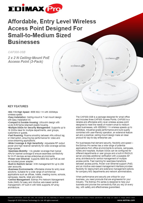
KEY FEATURES•802.11N High Speed: IEEE 802.11n with 300Mbps wireless speed.•Easy Installation: Ceiling-mount & T-rail mount design with easy installation kit.•Compact & Durable Housing: Ultra slim design withUL94-5VB flame-retardant plastic housing.•Multiple SSIDs for Security Management: Supports up to 16 SSIDs ideal for multiple departments, user groups, customers or guests.•Fast Roaming: Roams smoothly between APs without lag or interruption, ensuring top performance for video and voice streaming applications.•Wide Coverage & High Sensitivity: Adjustable RF output power and high receiver sensitivity for wide coverage across large spaces.•Seamless Mobility: 1.5x greater coverage than typical APs for blanket coverage to ensure seamless connectivity for Wi-Fi devices across enterprise environments.•Power over Ethernet: Supports IEEE 802.3af PoE as well as included power adapter.•Built-In RADIUS Server: With management for up to 256 user accounts.•Business Environments: Affordable choice for entry level solutions. Suitable for a wide range of commercial applications such as offices, hotels, meeting rooms, schools, campuses, resorts, retail and others.•Central Management: Edimax Pro Network Management Suite (NMS) for easy and Intuitive web-based central management. AP built-in with NMS supports AP array architecture.The CAP300-3SB is a package designed for small office and includes three CAP300 Access Points. CAP300 is a reliable and affordable entry level wireless access point designed to meet the needs of modern small to medium sized businesses, with IEEE802.11n wireless speeds up to 300Mbps. Industrial-grade performance and build quality combined with user-friendly operation, an extensive feature set and a practical, ceiling-mount design make an ideal product for day-to-day enterprise use.For businesses that demand security, flexibility and speed –the Edimax Pro series has a wide range of potential applications from office environments to schools, campuses, hotels and hospitals. Multiple SSIDs can be configured for different departments or user groups and a built-in RADIUS server provides additional verification with a scalable AP array architecture for central management of multiple access points. Fast roaming for seamless transitions between access points, Power over Ethernet support (PoE) and an intuitive web-based management interface provides flexibility for deployment and extensive management options for company MIS departments and network administrators. When performance and security are critical for your business, you need products that are engineered for your industry. The Edimax Pro series is designed to help your business and provide the connectivity that you rely on every day, with safety and effectiveness guaranteed.Affordable, Entry Level Wireless Access Point Designed For Small-to-Medium Sized BusinessesCAP300-3SB2 x 2 N Ceiling-Mount PoEAccess Point (3-Pack)SSID 1Finance Dept.SSID 2Sales Dept. SSID 3Guest RoomSSID 4 VoIPWide CoverageBYOD (Bring Your Own Device) Solution &High Density NetworkingFast RoamingHotels Offices Schools Hospitals2.4GHz2D Radiation Pattern@ HorizontalMultiple SSIDsSSID-9SSID-10SSID-11 SSID-14 SSID-15SSID-16SSID-13 SSID-12 SSID-1SSID-2 SSID-3 SSID-6SSID-7SSID-8SSID-5 SSID-4 Easy Installation KitCeiling mount and T-rail mount with bracket.2.4GHz2D Radiation Pattern@ VerticalCentral Network Management: NMSWork with Edimax Pro NMS (Network Management Suite)* web-based wireless network management software. Company MIS administrators can plan and manage Edimax Pro access points’ powerful functionalityaccording to their office space using an easy, remote web-based interface which includes a dashboard, map view, traffic statistics and wireless client list for network-wide remote administration. RADIUS settings, WLAN group settings, access control, guest network settings and firmware upgrades can all be managed centrally from a single location to reduce network downtime, aid troubleshooting and optimize network performance.Graphical zone plans with Google Maps integration and setup wizards are also available for expanding and managing large networks with multiple access points, with custom floor plans, visual overviews and easy drag-and-drop icons for quick access to key performance and monitoring information.*NMS is built-in with Edimax Pro CAP, WAP series & OAP1750 access point.Maximum performance, actual data rates, and coverage will vary depending on network conditions and environmental factors. Product specifications and design are subject to change without notice.Copyright © 2015 Edimax Technology Co. Ltd. All rights reserved.SPECIFICATIONS of CAP300 (single unit), CAP300-3SB includes 3 CAP3002 x 2 N Ceiling-Mount PoE Access PointRF SpecificationsFrequency Band •Radio Ⅰ: 802.11b/g/n 2.412~2.484(GHz)(The supported frequency band is restricted by local regulations.)Operation Channels •2.4GHz :US/Canada 1-11 / Europe 1-13 / Japan 1-14 Transmit Power(CE: 20dBm or lower, FCC:23dBm or lower)802.11b23dBm@1Mbps 23dBm@2Mbps *************23dBm@11Mbps802.11gn23dBm@6Mbps 23dBm@9Mbps 23dBm@12Mbps 23dBm@18Mbps 23dBm@24Mbps 22dBm@36Mbps 20dBm@48Mbps 19dBm@54Mbps802.11n26dBm@MCS0/MCS8 25dBm@MCS1/MCS9 25dBm@MCS2/MCS10 25dBm@MCS3/MCS11 24dBm@MCS4/MCS12 23dBm@MCS5/MCS13 22dBm@MCS6/MCS14 22dBm@MCS7/MCS15Receiver Sensitivity802.11b≤-95dBm@1Mbps ≤-90dBm@11Mbps802.11g≤-91dBm@6Mbps ≤-75dBm@54Mbps802.11n≤-93dBm@MCS0 ≤-73dBm@MCS7 ≤-90dBm@MCS8 ≤-70dBm@MCS15ManagementDeployment Standalone (AP mode)Master AP mode: Can manage 8 Edimax Pro APs with NMSManaged AP mode : Be managed by AP Controller (APC500), Edimax Pro Master AP with NMS softwareConfigurationHTTP/HTTPS SNMP v1, v2c, v3 CLI (Telnet, SSH)RADIUS Server Built-In Auto-Channel Y Private MIB YPackage Contents Access Point N300 Ceiling Mount PoE Access Point Mounting Bracket Ceiling-Mount & T-rail Mount Bracket KitPower Adapter 12V / 1A Power AdapterCableEthernet CableCD / Quick Installation Guide CD (User Manual & Multi-Language Quick Installation Guide) / Printed English QuickInstallation GuideAccessories OptionalGP-101IT IEEE802.3at PoE InjectorHardware LAN Interface Giga x 1PoE 802.3af (Supports 802.3at)Antenna Type: 2 x Built-In PIFA / Gain: 2.82dBi Max.Power DC: 12V / 1A802.3af (PoE Injector Optional)Dimensions 17.6 (D) x 3.2 (H) cmWeight287.3g Power Consumption (Full Loading) 6.5W Mounting CeilingReset YLED Indicator 1. Power LED 2. Diag LEDEnvironmental Conditions Operating Temperature: 0°C (32°F) to 50°C (122°F) Storage Temperature : -20°C (-4°F) to 60°C (140°F)Operating Humidity: 90% or Less Storage Humidity: 90% or LessPower Saving 802.3azInternal Buzzer YHousing UL94-5VB Flammability RatingWireless Standard 802.11 b/g/nNo. of Radios 1 Receiver Sensitivity ≤ -95dBm Certification CE/FCCFast Roaming Y Number of SSIDs 16 Performance Maximum Data Speed300Mbps Concurrent Clients Up to 50* Per RadioSecurity EncryptionWEP / WPA / WPA2Wireless L2 Isolation Y Station Isolation Y IEEE 802.1x AuthenticatorY EAP Authentication PEAP Hidden SSID Y MAC Address Filter Y Wireless STAY Rogue AP Detection (w/ NMS) YSoftware Wireless Mode AP / WDS AP / WDS Bridge802.1q VLAN Y (VID = 1-4095)Spanning Tree RSTP QoSWMM (802.11e) Max Associated Station No. Pass-Through IPv6 and VPN (PPTP, L2TP/IPsec)DSCP (802.1p)Y Multicast Rate up to 54MbpsY12V DC Power PortLAN Port with PoE INStatus LED Reset Button*The maximum users in 2.4GHz is depends on the interference condition of the environment.。
1952801资料
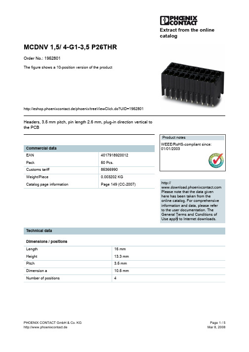
Extract from the onlinecatalogMCDNV 1,5/ 4-G1-3,5 P26THROrder No.: 1952801The figure shows a 10-position version of the producthttp://eshop.phoenixcontact.de/phoenix/treeViewClick.do?UID=1952801Headers, 3.5 mm pitch, pin length 2.6 mm, plug-in direction vertical to the PCBhttp://Please note that the data givenhere has been taken from theonline catalog. For comprehensiveinformation and data, please referto the user documentation. TheGeneral Terms and Conditions ofUse apply to Internet downloads. Technical dataDimensions / positionsLength16 mmHeight13.3 mmPitch 3.5 mmDimension a10.5 mmNumber of positions4Pin dimensions0,8 x 0,8 mm Pin spacing 3.5 mmHole diameter 1.3 mmTechnical dataInsulating material group IIIaRated surge voltage (III/3) 2.5 kVRated surge voltage (III/2) 2.5 kVRated surge voltage (II/2) 2.5 kVRated voltage (III/2)200 VRated voltage (II/2)250 V Connection in acc. with standard EN-VDE Nominal current I N8 ANominal voltage U N160 V Maximum load current8 A (per position) Insulating material LCP Inflammability class acc. to UL 94V0Certificates / ApprovalsApproval logoCULNominal voltage U N150 VNominal current I N8 AULNominal voltage U N150 VNominal current I N8 A Certification CUL, ULAccessoriesItem Designation DescriptionMarking0805030SK 3,5/2,8:SO Marker card, special printing, self-adhesive, labeled acc. tocustomer requirements, 14 identical marker strips per card, max.25-position labeling per strip, color: White0804109SK 3,81/2,8:FORTL.ZAHLEN Marker card, printed horizontally, self-adhesive, 10-section markerstrip, 14 identical decades marked 1-10, 11-20 etc. up to 91-(99)100, sufficient for 140 terminal blocksPlug/Adapter1734634CP-MSTB Coding profile, is inserted into the slot on the plug or invertedheader, red insulating materialDrawingsDrilling diagramDimensioned drawingAddressPHOENIX CONTACT GmbH & Co. KGFlachsmarktstr. 832825 Blomberg,GermanyPhone +49 5235 3 00Fax +49 5235 3 41200http://www.phoenixcontact.de© 2008 Phoenix ContactTechnical modifications reserved;。
电子知识大全
电子知识掌握了一下的硬件和软件知识,基本上就可以成为一个合格的电子工程师:第一部分:硬件知识一、数字信号1、TTL和带缓冲的TTL信号2、RS232和定义3、RS485/422(平衡信号)4、干接点信号二、模拟信号视频1、非平衡信号2、平衡信号三、芯片1、封装2、74073、74044、74005、74LS5736、ULN20037、74LS2448、74LS2409、74LS24510、74LS138/23811、CPLD(EPM7128)12、116113、max69114、max485/7517615、mc148916、mc148817、ICL232/max23218、89C51四、分立器件1、封装2、电阻:功耗和容值3、电容1)独石电容2)瓷片电容3)电解电容4、电感5、电源转换模块6、接线端子7、LED发光管8、8字(共阳和共阴)9、三极管2N555110、蜂鸣器五、单片机最小系统1、单片机2、看门狗和上电复位电路3、晶振和瓷片电容六、串行接口芯片1、eeprom2、串行I/O接口芯片3、串行AD、DA4、串行LED驱动、max7129七、电源设计1、开关电源:器件的选择2、线性电源:1)变压器2)桥3)电解电容3、电源的保护1)桥的保护2)单二极管保护八、维修1、电源2、看门狗3、信号九、设计思路1、电源:电压和电流2、接口:串口、开关量输入、开关量输出3、开关量信号输出调理1)TTL―>继电器2)TTL―>继电器(反向逻辑)3)TTL―>固态继电器4)TTL―>LED(8字)5)继电器―>继电器6)继电器―>固态继电器4、开关量信号输入调理1)干接点―>光耦2)TTL―>光耦5、CPU处理能力的考虑6、成为产品的考虑:1)电路板外形:大小尺寸、异形、连接器、空间体积2)电路板模块化设计3)成本分析4)器件的冗余度1.电阻的功耗2.电容的耐压值等5)机箱6)电源的选择7)模块化设计8)成本核算1.如何计算电路板的成本?2.如何降低成本?选用功能满足价格便宜的器件十、思考题1、如何检测和指示RS422信号2、如何检测和指示RS232信号3、设计一个4位8字的显示板1)电源:DC122)接口:RS2323)4位3”8字(连在一起)4)亮度检测5)二级调光4、设计一个33位1”8字的显示板1)电源:DC5V2)接口:RS2323)3排11位8字,分4个、3个、4个3组,带行与行之间带间隔4)单片机最小系统5)译码逻辑6)显示驱动和驱动器件5、设计一个PCL725和MOXA C168P的接口板1)电源:DC5V2)接口:PCL725/MOXA8个RS2321.PCL725,直立DB37,孔2.MOXA C168P,DB62弯3)开关量输出信号调理:6个固态继电器和8个继电器,可以被任何一路信号控制和驱动,接口:固态继电器5.08直立,继电器3.81直立4)开关量输入调理:干接点闭合为1或0可选,接口:3.81直立5)RS232调理:1.LED指示2.前4路RS232全信号,后4路只需要TX、RX、03.无需光电隔离4.接口形式:DB9(针)直立第二部分:软件知识一、汇编语言二、C51该部分可以从市场上买到的N种开发板上学到,至于第一部分,需要人来带吧。
C.N-1818中文规格书

深圳市菜鸟电子有限公司地址:深圳市龙华新区上油松村产品规格书产品型号.:C.N-1818版本号:X1.0客户:产品描述: Input:110~240V AC 50/60Hz Output:12VDC2A客户型号:样品编号:日期:1.范围 (4)2.电气规格 (4)2.1. 交流输入 (4)2.1.1.输入电压 (4)2.1.2. 输入频率 (4)2.1.3. 效率 (4)2.1.4. 待机功耗 (4)2.1.5. 浪涌电流 (4)2.1.6. 最大AC输入电流 (4)2.2. DC 输出 (4)2.2.1. 输出电压 (4)2.2.2. 输出过冲电压 (4)2.2.3. 输出电流 (5)2.2.4. 输出纹波和杂讯 (5)2.2.5. 输出开机;延时 (5)2.2.6. 过功率保护 (5)2.2.7. 保持时间 (5)2.2.8. 动态负载规则 (5)2.2.9. 短路保护 (5)3. 机械性能 (5)3.1. 外观尺寸 (5)4. 环境 (6)4.1. 温度和湿度 (6)4.2. 振动 (6)4.3. 落地试验 (6)4.4 EMI (6)4.4.1. 传导 (6)4.4.2. 辐射 (6)4.5. 产品温度 (6)5. 可靠性 (6)5.1平均无故障时间…….…………………………………………………………………………. .66. 安全测试 (7)6.1. Hi-Pot (7)6.2.绝缘测试 (7)6.3.泄漏电流 (7)7. ROHS (7)1. 范围本产品C.N-1818、24W为宽电压输入,单组直流电压输出的开关电源适配器2. 电器规格2.1. 交流输入2.1.1. 输入电压产品工作电压110-240VAC + 10% .2.1.2.输入频率47 到63 Hz.2.1.3. 效率本产品转换效率可达到75%以上, 输入115VAC/60HZ 输出满载的条件下.2.1.4. 待机功耗当产品输入电压为240VAC/50HZ输出为0A时,最大损耗为0.5W2.1.5. 浪涌电流产品在冷开机状态下输入电压为110VAC 90度角时50A MAX输入电压为240V AC90度角时50A MAX2.1.6最大输入AC电流0.8A @90Vac,0.4A @180Vac.2.2. DC 输出2.2.1. 输出电压在额定的电压和频率.连续输出电流的最小值和最大值如下表.输出电压的量测在输出末端.2.2.2. 输出过冲电压当产品输入电压为规格要求的最大或最小,输出为空载时,开机或关机瞬间的最大输出电压调节率不大于8%。
5821中文资料

BiMOS II 8-BIT SERIAL-INPUT,LATCHED DRIVERSAlways order by complete part number, e.g., UCN5821A .Data Sheet 26185.12E5821 AND 5822A merged combination of bipolar and MOS technology gives these devices an interface flexibility beyond the reach of standard logic buffers and power driver arrays. The UCN5821A,UCN5821LW, UCN5822A, and UCN5822LW each have an eight-bit CMOS shift register and CMOS control circuitry, eight CMOS data latches, and eight bipolar current-sinking Darlington output drivers. The UCN5821A/LW and UCN5822A/LW are identical except for rated output voltage.BiMOS II devices have much higher data-input rates than the original BiMOS circuits. With a 5 V logic supply, they will typically operate at better than 5 MHz. With a 12 V supply,significantly higher speeds are obtained. The CMOS inputs are compatible with standard CMOS and NMOS logic levels. TTL circuits may require the use of appropriate pull-up resistors. By using the serial data output, the drivers can be cascaded for interface applications requiring additional drive lines.The UCN5821/22A are furnished in a standard 16-pin plastic DIP; the UCN5821/22LW are in a 16-lead wide-body SOIC for surface-mount applications. The UCN5821A is also available for operation from -40°C to +85°C. To order, change the prefix from ‘UCN’ to ‘UCQ’.FEATURESI To 3.3 MHz Data Input Rate I CMOS, NMOS, TTL Compatible I Internal Pull-Down ResistorsI Low-Power CMOS Logic & Latches I High-Voltage Current-Sink Outputs I Automotive Capable5821 AND 58228-BIT SERIAL-INPUT,LATCHED DRIVERS115 Northeast Cutoff, Box 15036Worcester, Massachusetts 01615-0036 (508) 853-5000Copyright © 1985, 2000, Allegro MicroSystems, Inc.5821 AND 5822 8-BIT SERIAL-INPUT, LATCHED DRIVERS LimitsCharacteristic Symbol Test Conditions Min.Max.Units Output Leakage I CEX UCN5821A/LW, V OUT = 50 V—50µACurrent UCN5822A/LW, VOUT= 80 V—50µAUCN5821A/LW, V OUT = 50 V, T A = +70°C—100µAUCN5822A/LW, V OUT = 80 V, T A = +70°C—100µA Collector-Emitter V CE(SAT)I OUT = 100 mA— 1.1VSaturation Voltage IOUT= 200 mA— 1.3VI OUT = 350 mA, V DD = 7.0 V— 1.6V Input Voltage V IN(0)—0.8VV IN(1)V DD = 12 V10.5—VV DD = 5.0 V 3.5—V Input Resistance r IN V DD = 12 V50—kΩV DD = 5.0 V50—kΩSupply Current I DD(ON)One Driver ON, V DD = 12 V— 4.5mAOne Driver ON, V DD = 10 V— 3.9mAOne Driver ON, V DD = 5.0 V— 2.4mAI DD(OFF)V DD = 5.0 V, All Drivers OFF, All Inputs = 0 V— 1.6mAV DD = 12 V, All Drivers OFF, All Inputs = 0 V— 2.9mA ELECTRICAL CHARACTERISTICS at T A = +25°C, V DD = 5 V, (unless otherwise specified).5821 AND 58228-BIT SERIAL-INPUT,LATCHED DRIVERS115 Northeast Cutoff, Box 15036Worcester, Massachusetts 01615-0036 (508) 853-5000TIMING CONDITIONS(V DD = 5.0 V, T A = +25°C, Logic Levels are V DD and Ground)A.Minimum Data Active Time Before Clock Pulse(Data Set-Up Time).......................................................................75 ns B.Minimum Data Active Time After Clock Pulse(Data Hold Time)...........................................................................75 ns C.Minimum Data Pulse Width..............................................................150 ns D.Minimum Clock Pulse Width ............................................................150 ns E.Minimum Time Between Clock Activation and Strobe.......................30 ns F.Minimum Strobe Pulse Width...........................................................100 nsG.Typical Time Between Strobe Activation andOutput Transition ..........................................................................1.0 µsL = Low Logic Level H = High Logic Level X = Irrelevant P = Present State R = Previous StateDwg. No. A-12,627Serial Data present at the input is transferred to the shift register on the logic “0” to logic “1” transition of the CLOCK input pulse. On succeeding CLOCK pulses, the registers shift data information towards the SERIAL DATA OUTPUT. The SERIAL DATA must appear at the input prior to the rising edge of the CLOCK input waveform.Information present at any register is transferred to its respective latch when the STROBE is high (serial-to-parallel con-version). The latches will continue to accept new data as long as the STROBE is held high. Applications where the latches are bypassed (STROBE tied high)will require that the ENABLE input be high during serial data entry.When the ENABLE input is high, all of the output buffers are disabled (OFF)without affecting the information stored in the latches or shift register. With the ENABLE input low, the outputs are controlled by the state of the latches.CLOCKDATA INSTROBEENABLE OUT5821 AND 58228-BIT SERIAL-INPUT,LATCHED DRIVERSNOTES: 1.Lead thickness is measured at seating plane or below.2.Lead spacing tolerance is non-cumulative.3.Exact body and lead configuration at vendor’s option within limits shown.Dwg. MA-001-16A inDwg. MA-001-16A mmUCN5821A and UCN5822ADimensions in Inches (controlling dimensions)Dimensions in Millimeters(for reference only)5821 AND 58228-BIT SERIAL-INPUT,LATCHED DRIVERS115 Northeast Cutoff, Box 15036Worcester, Massachusetts 01615-0036 (508) 853-5000NOTES: 1.Lead spacing tolerance is non-cumulative.2.Exact body and lead configuration at vendor’s option within limits shown.UCN5821LW and UCN5822LWDimensions in Inches (for reference only)(controlling dimensions)5821 AND 5822 8-BIT SERIAL-INPUT, LATCHED DRIVERSThe products described here are manufactured under one or more U.S. patents or U.S. patents pending.Allegro MicroSystems, Inc. reserves the right to make, from time to time, such departures from the detail specifications as may be required to permit improvements in the performance, reliability, or manufacturability of its products. Before placing an order, the user is cautioned to verify that the information being relied upon is current.Allegro products are not authorized for use as critical components in life-support devices or systems without express written approval.The information included herein is believed to be accurate and reliable. However, Allegro MicroSystems, Inc. assumes no responsi-bility for its use; nor for any infringement of patents or other rights of third parties which may result from its use.5821 AND 58228-BIT SERIAL-INPUT,LATCHED DRIVERS115 Northeast Cutoff, Box 15036Worcester, Massachusetts 01615-0036 (508) 853-5000POWERINTERFACE DRIVERSFunctionOutput Ratings*Part Number †SERIAL-INPUT LATCHED DRIVERS8-Bit (saturated drivers)-120 mA 50 V‡58958-Bit350 mA 50 V58218-Bit350 mA 80 V58228-Bit350 mA 50 V‡58418-Bit 350 mA 80 V‡58428-Bit (constant-current LED d river)75 mA 17 V62758-Bit (DMOS d rivers)250 mA 50 V65958-Bit (DMOS drivers)350 mA 50 V‡6A5958-Bit (DMOS drivers)100 mA 50 V6B59510-Bit (active pull-d owns)-25 mA 60 V5810-F an d 6809/1012-Bit (active pull-downs)-25 mA 60 V5811 an d 681116-Bit (constant-current LED driver)75 mA 17 V627620-Bit (active pull-d owns)-25 mA 60 V5812-F an d681232-Bit (active pull-d owns)-25 mA 60 V5818-F an d 681832-Bit100 mA 30 V583332-Bit (saturate d d rivers)100 mA 40 V5832PARALLEL-INPUT LATCHED DRIVERS4-Bit350 mA 50 V‡58008-Bit -25 mA 60 V58158-Bit350 mA 50 V‡58018-Bit (DMOS d rivers)100 mA 50 V6B2738-Bit (DMOS d rivers)250 mA 50 V6273SPECIAL-PURPOSE DEVICESUnipolar Stepper Motor Translator/Driver 1.25 A 50 V‡5804A ressable 8-Bit Deco der/DMOS Driver 250 mA 50 V6259Addressable 8-Bit Decoder/DMOS Driver 350 mA 50 V‡6A259A ressable 8-Bit Deco d er/DMOS Driver 100 mA 50 V6B259A ressable 28-Line Deco d er/Driver 450 mA30 V6817*Current is maximum specified test condition, voltage is maximum rating. See specification for sustaining voltage limits.Negative current is defined as coming out of (sourcing) the output.†Complete part number includes additional characters to indicate operating temperature range and package style.‡Internal transient-suppression diodes included for inductive-load protection.。
EDI88512CA20CM中文资料
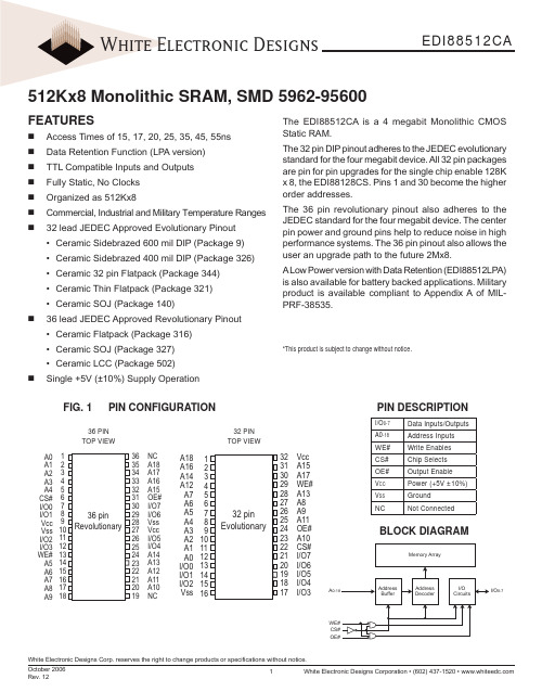
The EDI88512CA is a 4 megabit Monolithic CMOS Static RAM. The 32 pin DIP pinout adheres to the JEDEC evolutionary standard for the four megabit device. All 32 pin packages are pin for pin upgrades for the single chip enable 128K x 8, the EDI88128CS. Pins 1 and 30 become the higher order addresses. The 36 pin revolutionary pinout also adheres to the JEDEC standard for the four megabit device. The center pin power and ground pins help to reduce noise in high performance systems. The 36 pin pinout also allows the user an upgrade path to the future 2Mx8. A Low Power version with Data Retention (EDI88512LPA) is also available for battery backed applications. Military product is available compliant to Appendix A of MILPRF-38535.
*This product is subject to change without notice.
- 1、下载文档前请自行甄别文档内容的完整性,平台不提供额外的编辑、内容补充、找答案等附加服务。
- 2、"仅部分预览"的文档,不可在线预览部分如存在完整性等问题,可反馈申请退款(可完整预览的文档不适用该条件!)。
- 3、如文档侵犯您的权益,请联系客服反馈,我们会尽快为您处理(人工客服工作时间:9:00-18:30)。
256Kx8 Monolithic SRAMFEATURES256Kx8 CMOS Static Random Access Memory• Access Times of 70, 85, 100ns • Data Retention Function (LP Versions)• TTL Compatible Inputs and Outputs • Fully Static, No Clocks JEDEC Approved Pinout• 32 pin Ceramic DIP , 0.6 mils wide (Package 9)■Single +5V (±10%) Supply OperationFIGURE 1 – PIN CONFIGURATIONThe EDI88257C is a 2 Megabit 256Kx8 bit MonolithicCMOS Static RAM.The 32 pin DIP pinout adheres to the JEDEC standard for the two megabit device, and is a pin replacement for the 256Kx8 module, EDI88257C. The device is upgradeable to the 512Kx8 SRAM, the EDI88512C. Pin 1 becomes the higher order address.A Low Power version, EDI88257LP , offers a data retention function for battery back-up opperation. Military product is available compliant to Appendix A of MIL-PRF-38535.ABSOLUTE MAXIMUM RATINGSParameterValue Unit Voltage on any pin relative to Vss-0.5 to 7.0V Operating Temperature T A (Ambient) Industrial -40 to +85°C Military-55 to +125°C Storage Temperature, Plastic -65 to +150°C Power Dissipation 1W Output Current20mA Junction Temperature, T J175°CNOTE:Stress greater than those listed under “Absolute Maximum Ratings” may cause permanent damage to the device. This is a stress rating only and func t ion a l operation of the device at these or any other conditions greater than those in d i c at e d in the operational sections of this spec i fi c a t ion is not implied. Exposure to absolute maximum rating conditions for extended periods may affect reliability.RECOMMENDED OPERATING CONDITIONSParameter Symbol Min Typ Max Unit Supply Voltage V CC 4.5 5.0 5.5V Supply Voltage V SS 000V Input High Voltage V IH 2.2—V CC +0.5V Input Low VoltageV IL-0.3—+0.8VTRUTH TABLEG#E#W#Mode Output Power X H X Standby High Z I CC2, I CC3H L H Output DeselectHigh Z I CC1L L H Read Data Out I CC1XLLWriteData InI CC1DC CHARACTERISTICSV CC = 5V, T A = +25°CParameterSymbol Conditions Min Typ Max Units Input Leakage Current I LI V IN = 0V to V CC ——±10μA Output Leakage CurrentI LO V I/O = 0V to V CC——±10μA Operating Power Supply Current I CC1W#, E# = V IL , I I/O = 0mA, Min Cycle (70-100ns)—4575mA Standby (TTL) Power Supply Current I CC2E# ≥ V IH , V IN ≤ V IL , V IN ≥ V IH—310mA Full Standby Power Supply Current I CC3E# ≥ V CC -0.2VV IN ≥ Vcc -0.2V or V IN ≤ 0.2V C ——5mA LP ——1mA Output Low Voltage V OL I OL = 2.1mA ——0.4V Output High VoltageV OHI OH = -1.0mA2.4——VCAPACITANCEParameter Symbol ConditionMax Unit Address Lines C I V IN = Vcc or Vss, f = 1.0MHz 30pF Data LinesC OV OUT = Vcc or Vss, f = 1.0MHz14pFThese parameters are sampled, not 100% tested.AC CHARACTERISTICS – READ CYCLE V CC = 5.0V, Vss = 0V, -55°C T A+125°CParameterSymbol70ns85ns100nsUnits JEDEC Alt.Min Max Min Max Min MaxRead Cycle Time t AVAV t RC7085100ns Address Access Time t AVQV t AA7085100ns Chip Enable Access Time t ELQV t ACS7085100ns Chip Enable to Output in Low Z (1)t ELQX t CLZ101010ns Chip Disable to Output in High Z (1)t EHQZ t CHZ253030ns Output Hold from Address Change t AVQX t OH101010ns Output Enable to Output Valid t GLQV t OE354550ns Output Enable to Output in Low Z (1)t GLQX t OLZ555ns Output Disable to Output in High Z(1)t GHQZ t OHZ025030030ns 1. This parameter is guaranteed by design but not tested.AC CHARACTERISTICS – WRITE CYCLEV CC = 5.0V, V SS = 0V, -55°C T A+125°CParameterSymbol70ns85ns100nsUnits JEDEC Alt.Min Max Min Max Min MaxWrite Cycle Time t AVAV t WC7085100nsChip Enable to End of Write t ELWHt ELEH t CWt CW606070708080nsnsAddress Setup Time t AVWLt AVEL t ASt ASnsnsAddress Valid to End of Write t AVWHt AVEH t AWt AW656570708080nsnsWrite Pulse Width t WLWHt WLEH t WPt WP505055556060nsnsWrite Recovery Time t WHAXt EHAX t WRt WRnsnsData Hold Time t WHDXt EHDX t DHt DHnsnsWrite to Output in High Z (1)t WLQZ t WHZ025030030nsData to Write Time t DVWHt DVEH t DWt DW403040354040nsnsOutput Active from End of Write (1)t WHQX t WLZ500ns 1. This parameter is guaranteed by design but not tested.FIGURE 2 – TIMING WAVEFORM - READ CYCLEDATA RETENTION CHARACTERISTICS (EDI88257LP ONLY)-55°C T A+125°CCharacteristicLow Power Version onlySym Conditions Min Typ Max UnitsData Retention VoltageData Retention Quiescent Current V CCI CCDRV CC = 2.0VE# ≥ V CC -0.2V2––––185VμAChip Disable to Data Retention Time Operation Recovery Time t CDRT RV IN≥ V CC -0.2Vor V IN≤ 0.2Vt AVAV––––nsnsFIGURE 5 – DATA RETENTION - E# CONTROLLEDPACKAGE 9: 32 PIN SIDEBRAZED CERAMIC DIP (600MILS WIDE)ALL DIMENSIONS ARE IN INCHESORDERING INFORMATIONEDI 8 8 257 C X X XWHITE ELECTRONIC DESIGNSSRAMORGANIZATION, 256Kx8TECHNOLOGY:C = CMOS Standard PowerLP = Low PowerACCESS TIME (ns)PACKAGE TYPE:C = 32 lead Sidebrazed DIP, 600 mil (Package 9)DEVICE GRADE:B =MIL-STD-883 CompliantM = Military Screened -55°C to +125°CI = Industrial -40°C to +85°CC =Commercial 0°C to +70°C。