NBB-500-T1;中文规格书,Datasheet资料
MMBT5401-TP;中文规格书,Datasheet资料
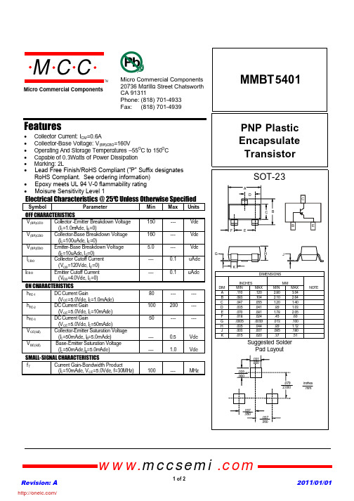
MMBT5401PNP Plastic Encapsulate TransistorFeatures• Collector Current:I CM =0.6A• Collector-Base Voltage:V (BR)CBO =160V• Operating And Storage Temperatures –55O C to 150O C • Capable of 0.3Watts of Power Dissipation • Marking:2LElectrical Characteristics @ 25OC Unless Otherwise SpecifiedSymbol ParameterMin Max Units OFF CHARACTERISTICSV (BR)CEO Coll e ctor -Emitter Breakdown Voltage (I C =1.0m Adc,I B =0)150--- Vdc V (BR)CBO Collector-Base Breakdown Voltage (I C =100uAdc,I E =0)160--- Vdc V (BR)EBO Emitter-Base Breakdown Voltage (I E =10uAdc,I C =0) 5.0--- VdcI CBO Collector Cutoff Current (V CB =120Vdc,I E =0)---0.1uAdcI EBOEmitter Cutoff Current (V EB =4.0Vdc,I C =0)---0.1uAdcON CHARACTERISTICSh FE-1DC Current Gain(V CE =5.0Vdc,I C =1.0mAdc)80------ h FE-2DC Current Gain(V CE =5.0Vdc,I C =10mAdc)100200--- h FE-3DC Current Gain(V CE =5.0Vdc,I C =50mAdc)50------V CE(sat)Collector-Emitter Saturation Voltage (I C =50mAdc,I B =5.0mAdc)---0.5Vdc V BE(sat)Base-Emitter Saturation Voltage (I C =50mAdc,I B =5.0mAdc)---1.0VdcSMALL-SIGNAL CHARACTERISTICSf TCurrent Gain-Bandwidth Product(I C =10mAdc,V CE =5.0Vdc, f=30MHz)100---MHzRevision: A 2011/01/01omp onents 20736Marilla Street Chatsworth! "# $ % ! "#Micro Commercial Componentswww.mccsemi .com1 of 2• Lead Free Finish/RoHS Compliant ("P" Suffix designates RoHS Compliant. See ordering information)• Epoxy meets UL 94 V-0 flammability rating • Moisure Sensitivity Level 1/Revision: A 2011/01/01Micro Commercial Componentswww.mccsemi .com2 of 23Ordering Information :***IMPORTANT NOTICE***Micro Commercial Components Corp. reserve s the right to make changes without further notice to any product herein to make corrections, modifications , enhancements , improvements , or other changes . Micro Commercial Components Corp . does not assume any liability arising out of the application or use of any product described herein; neither does it convey any license under its patent rights ,nor the rights of others . The user of products in such applications shall assume all risks of such use and will agree to hold Micro Commercial Components Corp . and all the companies whose products are represented on our website, harmless against all damages.***LIFE SUPPORT***MCC's products are not authorized for use as critical components in life support devices or systems without the express writtenapproval of Micro Commercial Components Corporation.***CUSTOMER AWARENESS***Counterfeiting of semiconductor parts is a growing problem in the industry. Micro Commercial Components (MCC) is taking strong measures to protect ourselves and our customers from the proliferation of counterfeit parts. MCC strongly encourages customers to purchase MCC parts either directly from MCC or from Authorized MCC Distributors who are listed by country on our web page cited below . Products customers buy either from MCC directly or from Authorized MCC Distributors are genuine parts, have full traceability, meet MCC's quality standards for handling and storage. MCC will not provide any warranty coverage or other assistance for parts bought from Unauthorized Sources. MCC is committed to combat this global problem and encourage our customers to do their part in stopping this practice by buying direct or from authorized distributors.DevicePackingPart Number-T PTape&Reel;3Kpcs/Reel/分销商库存信息: MICRO-COMMERICAL-CO MMBT5401-TP。
RTC-8564JEB3ROHS;RTC-8564NBB3ROHS;RTC-8564JE0ROHS;RTC-8564NBB0ROHS;中文规格书,Datasheet资料

CLKOUT CLKOE
Hours OUTPUT CONTROL DIVIDER Days Weekdays Month / Century Years
32.768 kHz frequency output function
•CLKOUT pin output (C-MOS output ), CL=30 pF •CLKOE pin enables output on/off control. •Output selectable <32.768kHz,1024Hz,32Hz,1Hz>
12.
6.00.2
11.
5.00.2
/INT VDD GND
Output -
Interrupt output
(N-ch open drain)
VSOJ20 pin
SON22 pin
VSOJ12pin
Connected to a positive power supply. Connected to a ground.
Unit
fSCL=0Hz
IBK CLKOUT;
CLKOE=GND
nA 275 700
VDD output OFF(LOW ) =3V VDD =5V
Condition Ta=-20C+70C Ta=-40 C+85C Ta=-20C+70C Ta=-40 C+85C
GND (GND) N.C. SDA SCL CLKOUT VDD CLKOE N.C. N.C.
17. 16. 15.
19. 18. 17.
Output
3. 4. 5. 6.
N.C. N.C. /INT GND
500 Series Diode Bridge Compressor 产品说明书
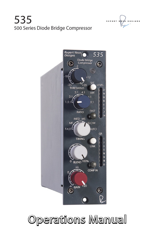
535500 Series Diode Bridge CompressorOperations Manual1. Read these instructions.2. Keep these instructions.3. Heed all warnings.4. Follow all instructions.5. Do not use this apparatus near water.6. Clean only with a dry cloth.7. Do not block any ventilation openings. Install in accordance with themanufacturer’s instructions.8. Do not install near any heat sources such as radiators, heat registers, stoves, or other apparatus (including amplifiers) that produce heat.9. Do not defeat the safety purpose of the polarized or grounding-typeplug. A polarized plug has two blades with one wider than the other.A grounding-type plug has two blades and a third grounding prong.The wide blade or the third prong are provided for your safety. If theprovided plug does not fit into your outlet, consult an electrician forreplacement of the obsolete outlet.10. Protect the power cord from being walked on or pinched particularly atplugs, convenience receptacles, and the point where they exit from theapparatus.11.12. Use only with a cart, stand, tripod, bracket, orthe apparatus. When a cart is used, use cautionavoid injury from tip-over.13. when unused for long periods of time.14. Refer all servicing to qualified service personnel. Servicing is requiredwhen the apparatus has been damaged in any way, such as power-supply cord or plug is damaged, liquid has been spilled or objects have fallen into the apparatus, the apparatus has been exposed to rain or moisture, does not operate normally, or has been dropped.15. This apparatus shall not be exposed to dripping or splashing, and noobject filled with liquids, such as vases or beer glasses, shall be placed on the apparatus.16. Do not overload wall outlets and extension cords as this can result in a risk of fire or electric shock.17. This apparatus has been designed with Class-I construction and mustbe connected to a mains socket outlet with a protective earthingconnection (the third grounding prong).18. This apparatus has been equipped with a rocker-style AC mains power switch. This switch is located on the rear panel and should remainreadily accessible to the user.19. The MAINS plug or an appliance coupler is used as the disconnect device, so the disconnect device shall remain readily operable.20. N OTE: This equipment has been tested and found to comply with the limits for a Class B digital device, pursuant to part 15 of the FCC Rules. These limits are designed to provide reasonable protection against harmful interference in a residential installation. This equipment generates, uses, and can radiate radio frequency energy and, if not installed and used in accordance with the instructions, may cause harmful interference to radio communications. However, there is no guarantee that interference will not occur in a particular installation. If this equipment does cause harmful interference to radio or televisionreception, which can be determined by turning the equipment o and on, the user is encouraged to try to correct the interference by one or more of the following measures:• Reorient or relocate the receiving antenna.• Increase the separation between the equipment and the receiver.• Connect the equipment into an outlet on a circuit different from that to which the receiver is connected.• Consult the dealer or an experienced radio/TV technician for help. CAUTION: Changes or modifications to this device not expressly approved by Rupert Neve Designs LLC, could void the user's authority to operate the equipment under FCC rules.21. This apparatus does not exceed the Class A/Class B (whichever is applicable) limits for radio noise emissions from digital apparatus as set out in the radio interference regulations of the Canadian Department of Communications.ATTENTION — Le présent appareil numérique n’émet pas de bruits radioélectriques dépassant las limites applicables aux appareils numériques de class A/de class B (selon le cas) prescrites dans le réglement sur le brouillage radioélectrique édicté par les ministere des communications du Canada.22. Exposure to extremely high noise levels may cause permanent hearing loss. Individuals vary considerably in susceptibility to noise-induced hearing loss, but nearly everyone will lose some hearing if exposed tosufficiently intense noise for a period of time. The U.S. Government’s Occupational Safety and Health Administration (OSHA) has specifiedthe permissible noise level exposures shown in the following chart. According to OSHA, any exposure in excess of these permissible limits could result in some hearing loss. To ensure against potentially dangerous exposure to high sound pressure levels, it is recommended that all persons exposed to equipment capable of producing highsound pressure levels use hearing protectors while the equipment is in operation. Ear plugs or protectors in the ear canals or over the ears must be worn when operating the equipment in order to preventpermanent hearing loss if exposure is in excess of the limits set forth here:Important Safety InstructionsWARNING — To reduce the risk of fire or electric shock, do notexpose this apparatus to rain or moisture.Duration, per day in hours Sound Level dBA, Slow Response Typical Example 890Duo in small club 692495Subway Train3972100 Typical music via head phones 1.51021105Siren at 10 m distance 0.51100.25 or less 115Loudest parts at a rock concert535 Diode Bridge CompressorThank you for your purchase of the 535 Diode Bridge Compressor. We hope you enjoy using this tool as much as we have enjoyed designing it. Please read through the entire manual before attempting to setup or operate your 535 Diode Bridge Compressor.535 Design NotesRupert Neve’s original 2254 compressor served as an inspiration for the design of the 535. Understanding that there were limitations to the original 2254 topology, painstaking effort was taken to reproduce the desirable qualities of the 2254 while improving the original device’s elevated noise floor, inflexible attack time constants, limited range of threshold and ratio controls, and low saturation headroom.The updated compressor design employs full-wave rectification in the sidechain to help minimize the effects of intermodulation distortion in the main audio path, while maintaining the tonality that made the original 2254 famous. Using a diode bridge as a gain control element in a compressor produces a unique sonic character, and it was imperative for the new compressor to deliver what the vintage device inspired.In addition to full-wave rectification in the compressor sidechain path, the TIMING controls have been expanded. Each of the six selectable settings have been chosen for different dynamic applications, including FAST and MF mode for more transient signals to SLOW and AUTO for more generalized applications. Combine this control set with the FAST switch, and the available TIMING control settings have been doubled from 6 to 12.Previous Rupert Neve Designs compressors like the 543 and Portico II series have been about transparency: the 535 is about punch, vibe, and color. The character of the Diode Bridge in combination with an upgraded feature set provide a versatile update to a vintage compressor topology for the modern studio engineer.535 FeaturesThresholdThe THRESHOLD control has 31 detents and allows the user to adjust the point at which compression begins, between -25dBu and +20dBu. Turning this control counter-clockwise will increase the amount of compression; turning it clockwise will decrease the amount of compression. If the input signal is lower than the set threshold, no compression will occur.It is advisable to start with this control set fully clockwise, and set the other controls first. Once the other controls are set to the desired values, slowly bring the THRESHOLD control down (turning counter-clockwise), while listening carefully until the optimal amount of compression is achieved for the givensource material.GR MeterEight segment LED meter that indicates gain reduction.Level MeterEight segment LED meter that indicates output level.Gain31 detent pot thatadjusts output gain from -6dB to +20dB.Comp InSwitch that inserts the compressor into the audio path.FastSwitch that divides the compressor attack and release times in half.LinkSwitch that allowsmultiple modules to be operated in stereo.S/C HPFSwitch that inserts a 150Hz high pass in the compressor sidechain.Blend31 detent pot that adjusts the mix of compressed and uncompressed signal.TimingSix posi�on rotary switch that sets the compressor a�ack andrelease �mes.Ra�oSix posi�on rotary switch that sets the slope of compressionfrom 1.5:1 to 8:1.Threshold31 detent pot that sets the level at which compression begins from -25dB to +20dB.The RATIO control has 6 selectable positions on the rotary switch and allows the user to set the slope of the compressor curve, with pre-selected ratios of 1.5:1 through 8:1. This range of compression ratios allows the user to compress very moderately, or if desired, dole out heavy compression to achieve an intentional effect on higher ratio settings.TimingThe TIMING control allows the user to change the attack and release times simultaneously for the diode bridge compressor. Each TIMING setting has a different attack and release time constant. Due to the nature of this topology, these time constants will adapt themselves slightly depending on several factors: compression ratio, threshold, and source material. This allows the diode bridge compressor to remain flexible with various types of source material. We encourage the user to experiment with different combinations of ratio, timing, and threshold settings to achieve the desired compression on the signal.FAST Fast Attack (750us), Fast Release (130ms)MF Medium Attack (2.25ms), Fast Release (130ms)MED Medium Attack (2.25ms), Medium Release (400ms)MS Medium Attack (4ms), Slow Release (725ms)SLOW Slow Attack (10ms), Slow Release (1S)AUTO Medium Attack (5ms), Dual Decay Release (T1 500ms, T2 1s) GainThe GAIN control has 31 detents and allows the user to add gain to the compressed signal in order to bring the signal level back up to unity with the uncompressed input signal. It is much easier to evaluate the tonal effect of the compressor when the compressed output level is matched to the uncompressed input level, thereby eliminating the misleading level difference.BlendThe BLEND control has 31 detents and allows the user to mix the uncompressed (dry) signal with compressed (wet) signal. Turning the control towards 0% will shift the mix to fully uncompressed dry signal, whereas turning the control towards 100% will shift the mix to the fully compressed signal. This feature allows for parallel compression by blending the direct and compressed signals, enabling a wider range of compression subtlety.The FAST switch divides the attack and release times available on the TIMING control in half, effectively doubling the number of TIMING presets available to the user.LinkThe LINK switch allows the compressor to be linked to another 535 compressor module via a sidechain control voltage. In link mode, the compressor generating the greater sidechain voltage (resulting in higher amounts of compression) will control the compression of both audio signal paths to maintain proper stereo image while compressing.Sidechain HPFThe S/C HPF switch allows the user to insert a 150Hz high-pass filter in the compressor sidechain. When this filter is engaged, the compressor will be considerably less responsive to information below 150Hz. As an example, if used on a drum kit, the low end of the kick drum would be less compressed than the snare drum or cymbals since a significant portion of the kick drum’s dynamic energy is focused below 150Hz.Comp InThe COMP IN switch allows the user to audition the compression. By disengaging the COMP IN switch, the compressor is bypassed and the user can quickly compare the sound of the dry input signal for an objective evaluation of the sonic effect of the compressor on the audio signal. COMP IN can be used in combination with the GAIN control to match the perceived level of the compressed audio signal with the level of the uncompressed input signal.Level and Gain Reduction MeteringThese two LED meters are provided to give an accurate representation of the output level of the compressor, as well as the amount of gain reduction being applied to the input signal.Operation GuideUnderstanding the signal paths involved in creating an accurate gain control device is an important step to using a compressor effectively. At the heart of the 535 is a Diode Bridge, manipulated by a control voltage which is generated by the compressor sidechain. The purpose of a compressor sidechain is to convert the input audio signal into the corresponding control voltage. Within the sidechain, several controls are available to the user including THRESHOLD, RATIO and TIMING. Using these controls, the user can manipulate the sidechain signal at key points to achieve proper control over the main audio path. The sidechain for this compressor receives audio input from a point immediately after the Diode Bridge, making it a feedback-style compressor.The 535 compressor sidechain has been upgraded with a Full-Wave rectifier rather than the Half-Wave detector of past Diode Bridge designs. This guarantees lower overall intermodulation distortion and faster available attack times in comparison to the original. This compressor was designed with the ability to “color” the audio passing through it; this can be achieved in the following ways: The first method is using higher input levels, which cause the Diode Bridge gain reduction element to produce its own harmonic content, regardless of whether the compressor is compressing the audio signal or not. This harmonic threshold has been set to +20dBu (to correspond with the maximum THRESHOLD control setting), allowing most signals to pass unaffected. However if desired, the user can drive the compressor input harder in order to bring out the more aggressive tonal characteristics. These harmonics are independent of frequency, and they increase exponentially beyond +20dBu. We encourage the user to experiment with varying input levels to find the right tonal shaping for the given source material.The second method is using higher RATIO and faster TIMING control settings. Faster TIMING settings will smooth the compressor control voltage less, and therefore induce more harmonic content, as peak to peak control voltage ripple will be greater. This will translate to more color in the main audio path. Slower TIMING settings will smooth the control voltage significantly, and thereby reduce the harmonic content added to the audio path, resulting in more transparent compression. The harmonic content created in this way is what contributes to the Diode Bridge Compressor’s renowned warm character.R a ti o C u r v e sI n p u tO u t p u tL e g e n dR A T I O S e tti n g s 1:1 (B Y P A S S ) 1.5:12:13:14:16:18:1T h e r a ti o c u r v e s s h o w n a b o v e w e r e t a k e n w i t h T H R E S H O L D s e t t o t h e f o l l o w i n g v a l u e s :-25d B u -10d B u 0d B u +10d B uOperation Guide ContinuedHaving covered some of the ways in which this compressor can be used to color the audio signal, it is important to note that this compressor can also be utilized in more transparent applications. There are several methods that can be used individually or in combination for increased compression subtlety:- Lower RATIO control settings (1.5:1, 2:1, 3:1)- Slower TIMING control settings (MS, SLOW, AUTO)- Engaging S/C HPF to remove low frequency compression- Utilizing the BLEND control to mix the uncompressed signal with compressed signal (parallel compression)The range of attack and release times that can be achieved across the various RATIO settings is quite wide, and is useful for dialing in the proper compression envelope. Due to the nature of the charge and discharge characteristics of the timing networks in this compressor, there is an inherent flexibility in the timing range for each of the six switch positions on the TIMING control.Limited WarrantyRupert Neve Designs warrants this product to be free from defects in materials and workmanship for a period of one (1) year from date of purchase, and agrees to remedy any defect identified within that period by, at our option, repairing or replacing the product.Limitations and ExclusionsThis warranty, and any other express or implied warranty, does not apply to any product which has been improperly installed, subjected to usage for which the product was not designed, misused or abused, damaged during shipping, damaged by any dry cell batter, or which has been altered or modified in any way. This warranty is extended to the original end user purchaser only. A purchase receipt or other satisfactory proof of original purchase is required before any warranty service will be performed. THIS EXPRESS, LIMITED WARRANTY IS IN LIEU OF ALL OTHER WARRANTIES, EXPRESS OR IMPLIED, TO THE EXTENT ALLOWED UNDER APPLICABLE STATE LAW. IN NO EVENT SHALL RUPERT NEVE DESIGNS BE LIABLE FOR ANY SPECIAL, INCIDENTAL, OR CONSEQUENTIAL DAMAGES RESULTING FROM THE USE OF THIS PRODUCT. Some states do not allow the exclusion or limitation of consequential damages or limitations on how long an implied warranty lasts, so this exclusion may not apply to you.Warranty ServiceI f you suspect a defect in your device, please call us at 512-847-3013 or contact our support staff (**********************)for troubleshooting. If it is determined that the device is malfunctioning, we will issue a Return Material Authorization and provide instructions for shipping the device to our service department.Rupert Neve DesignsPO Box 1969Wimberley TX 78676tel: +1 512-847-3013fax: +1 512-847-8869PN: 775-00028 revB。
NBB-402-E资料

Product DescriptionOrdering InformationTypical ApplicationsFeaturesFunctional Block DiagramRF Micro Devices, Inc.7628 Thorndike Road Greensboro, NC 27409, USA Tel (336) 664 1233Fax (336) 664 0454 Optimum Technology Matching® AppliedSi BJTGaAs MESFET GaAs HBT Si Bi-CMOSSiGe HBT Si CMOS InGaP/HBTGaN HEMTSiGe Bi-CMOSPin 1GroundRF INGroundCASCADABLE BROADBANDGaAs MMIC AMPLIFIER DC TO 8GHz•Narrow and Broadband Commercial and Military Radio Designs•Linear and Saturated Amplifiers •Gain Stage or Driver Amplifiers for MWRadio/Optical Designs (PTP/PMP/LMDS/UNII/VSA T/WLAN/Cellular/DWDM)The NBB-402 cascadable broadband InGaP/GaAs MMIC amplifier is a low-cost, high-performance solution for gen-eral purpose RF and microwave amplification needs. This 50Ω gain block is based on a reliable HBT proprietary MMIC design, providing unsurpassed performance for small-signal applications. Designed with an external bias resistor, the NBB-402 provides flexibility and stability. The NBB-402 is packaged in a low-cost, surface-mount ceramic package, providing ease of assembly for high-volume tape-and-reel requirements.•Reliable, Low-Cost HBT Design •15.0dB Gain, +15.8dBm P1dB@2GHz •High P1dB of +15.4dBm@6.0GHz •Single Power Supply Operation•50Ω I/O Matched for High Freq. UseNBB-402Cascadable Broadband GaAs MMIC Amplifier DC to 8GHzNBB-402-T1 or -T3Tape & Reel, 1000 or 3000 Pieces (respectively)NBB-402-E Fully Assembled Evaluation Board NBB-X-K1Extended Frequency InGaP Amp Designer’s Tool Kit Notes:1. Solder pads are coplanar to within ±0.025 mm.2. Lid will be centered relative to frontside metallization with a tolerance of ±0.13 mm.3. Mark to include two characters and dot to reference pin 1.Package Style: MPGA, Bowtie, 3x3, Ceramic9Absolute Maximum RatingsParameterRatingUnitRF Input Power +20dBm Power Dissipation 300mW Device Current70mA Channel T emperature 200°C Operating Temperature -45 to +85°C Storage Temperature-65 to +150°CExceeding any one or a combination of these limits may cause permanent damage.ParameterSpecification UnitConditionMin.Typ.Max.OverallV D =+3.9V, I CC =47mA, Z 0=50Ω, T A =+25°C Small Signal Power Gain, S2115.017.1dB f=0.1GHz to 1.0GHz 15.8dB f=1.0GHz to 4.0GHz 14.3dB f=4.0GHz to 6.0GHz 12.012.5dB f=6.0GHz to 8.0GHz Gain Flatness, GF±0.8dBf=0.1GHz to 5.0GHz Input and Output VSWR1.45:1f=0.1GHz to 4.0GHz 1.30:1f=4.0GHz to 8.0GHz 1.80:1f=8.0GHz to 10.0GHz Bandwidth, BW 6.3GHz BW3 (3dB)Output Power @-1dB Compression, P1dB15.8dBm f=2.0GHz 15.4dBm f=6.0GHz 15.5dBm f=8.0GHz Noise Figure, NF4.3dB f=3.0GHz Third Order Intercept, IP3+26.0dBm f=2.0GHzReverse Isolation, S12-17.5dB f=0.1GHz to 12.0GHzDevice Voltage, V D 3.6 3.9 4.2V Gain Temperature Coefficient,δG T /δT-0.0015dB/°CMTTF versus Temperature @ I CC =50mACase T emperature 85°C Junction Temperature 120.9°C MTTF>1,000,000hours Thermal ResistanceθJC 196°C/WJ T T CASE–V D I CC⋅--------------------------θJC °C Watt ⁄()= ESD sensitive device.RF Micro Devices believes the furnished information is correct and accurate at the time of this printing. However, RF Micro Devices reserves the right to make changes to its products without notice. RF Micro Devices does not assume responsibility for the use of the described product(s).Typical Bias ConfigurationApplication notes related to biasing circuit, device footprint, and thermal considerations are available on request.Application NotesDie AttachThe die attach process mechanically attaches the die to the circuit substrate. In addition, it electrically connects the ground to the trace on which the chip is mounted, and establishes the thermal path by which heat can leave the chip.Wire BondingElectrical connections to the chip are made through wire bonds. Either wedge or ball bonding methods are acceptable practices for wire bonding.Assembly ProcedureEpoxy or eutectic die attach are both acceptable attachment methods. T op and bottom metallization are gold. Conductive silver-filled epoxies are recommended. This procedure involves the use of epoxy to form a joint between the backside gold of the chip and the metallized area of the substrate. A 150°C cure for 1 hour is necessary. Recommended epoxy is Ablebond 84-1LMI from Ablestik.Bonding Temperature (Wedge or Ball)It is recommended that the heater block temperature be set to 160°C±10°C.Recommended Bias Resistor ValuesSupply Voltage, V CC(V)5810121520Bias Resistor, R CC (Ω)2281122162222322InV D = 3.9 VExtended Frequency InGaP Amplifier Designer’s Tool KitNBB-X-K1This tool kit was created to assist in the design-in of the RFMD NBB- and NLB-series InGap HBT gain block amplifiers. Each tool kit contains the following.• 5 each NBB-300, NBB-310 and NBB-400 Ceramic Micro-X Amplifiers• 5 each NLB-300, NLB-310 and NLB-400 Plastic Micro-X Amplifiers• 2 Broadband Evaluation Boards and High Frequency SMA Connectors•Broadband Bias Instructions and Specification Summary Index for ease of operationTape and Reel DimensionsAll Dimensions in Millimeters330 mm (13") REELMicro-X, MPGASYMBOL SIZE (mm)ITEMSSIZE (inches)FLANGE B T F 330 +0.25/-4.018.4 MAX 12.4 +2.0DiameterThicknessSpace Between Flange13.0 +0.079/-0.1580.724 MAX 0.488 +0.08HUBO S A 102.0 REF 13.0 +0.5/-0.21.5 MIN Outer DiameterSpindle Hole Diameter Key Slit Width D20.2 MINKey Slit Diameter4.0 REF0.512 +0.020/-0.0080.059 MIN0.795 MINUser Direction of FeedAo = 3.6 MM Bo = 3.6 MM Ko = 1.7 MMNOTES:1. 10 sprocket hole pitch cumulative tolerance ±0.2.2. Camber not to exceed 1 mm in 100 mm.3. Material: PS+C4. Ao and Bo measured on a plane 0.3 mm above the bottom of the pocket.5. Ko measured from a plane on the inside bottom of the pocket to the surface of the carrier.6. Pocket position relative to sprocket hole measured as true position of pocket, not pocket hole.Device Voltage versus Amplifier Current35.0040.0045.0050.0055.0060.00Amplifier Current, I CC (mA)P1dB versus Frequency at 25°C0.05.010.015.020.02.04.06.08.010.012.0Frequency (GHz)P 1d B (d B m )P OUT /Gain versus P IN at 2 GHz0.02.04.06.08.010.012.014.016.018.0-14.0-9.0-4.01.06.0P IN (dBm)P O U T (d B m ), G a i n (d B )Third Order Intercept versus Frequency at 25°C0.05.010.015.020.025.030.02.03.04.05.06.07.08.09.010.011.012.0Frequency (GHz)O u t p u t I P 3 (d B m )Note: The s-parameter gain results shown below include device performance as well as evaluation board and connector loss variations. The insertion losses of the evaluation board and connectors are as follows:1GHz to 4GHz=-0.06dB 5GHz to 9GHz=-0.22dB 10GHz to 14GHz=-0.50dB15GHz to 20GHz=-1.08dBS11 versus Frequency-20.0-15.0-10.0-5.00.00.05.010.015.020.0Frequency (GHz)S 11 (d B)S12 versus Frequency-25.0-20.0-15.0-10.0-5.00.00.05.010.015.020.0Frequency (GHz)S 12 (d B)S21 versus Frequency0.05.010.015.020.00.05.010.015.020.0Frequency (GHz)S 21 (d B)S22 versus Frequency-20.0-15.0-10.0-5.00.00.05.010.015.020.0Frequency (GHz)S 22 (d B )。
NBB-310-T1;NBB-310-PCK;中文规格书,Datasheet资料

7628 Thorndike Road, Greensboro, NC 27409-9421 · For sales or technical support, contact RFMD at (+1) 336-678-5570 or customerservice@.
1 of 11
Optimum Technology Matching® Applied
DS120130
GaAs HBT GaAs MESFET InGaP HBT
SiGe BiCMOS Si BiCMOS SiGe HBT
GaAs pHEMT Si CMOS Si BJT
GaN HEMT BiFET HBT LDMOS
/
NBB-310
Absolute Maximum Ratings Parameter
RF Input Power Power Dissipation Device Current Channel Temperature Operating Temperature Storage Temperature
Exceeding any one or a combination of these limits may cause permanent damage.
Parameter
Overall
Small Signal Power Gain, S21
Min.
12.5 12.0 11.0 9.0
Specification Typ.
Gain Flatness, GF Input and Output VSWR
Bandwidth, BW Output Power @ -1dB Compression, P1dB
NBB-400中文资料

RF Micro Devices, Inc.
Tel (336) 664 1233
7628 Thorndike Road
Fax (336) 664 0454
Greensboro, NC 27409, USA
4-33
元器件交易网
NBB-400
• Linear and Saturated Amplifiers
• Gain Stage or Driver Amplifiers for MWRadio/Optical Designs (PTP/PMP/ LMDS/UNII/VSAT/WLAN/Cellular/DWDM)
Product Description
δGT/δT
MTTF versus Temperature @ ICC=50mA
Case Temperature Junction Temperature MTTF
Thermal Resistance
θJC
Specification
Min.
Typ.
Max.
15.5
16.7
16.5
16.0
12.5
13.5
The NBB-400 cascadable broadband InGaP/GaAs MMIC amplifier is a low-cost, high-performance solution for general purpose RF and microwave amplification needs. This 50Ω gain block is based on a reliable HBT proprietary MMIC design, providing unsurpassed performance for small-signal applications. Designed with an external bias resistor, the NBB-400 provides flexibility and stability. The NBB-400 is packaged in a low-cost, surface-mount ceramic package, providing ease of assembly for highvolume tape-and-reel requirements. It is available in either packaged or chip (NBB-400-D) form, where its gold metallization is ideal for hybrid circuit designs.
MMBT5401高电压PNP Silicon M5A艾克拉特透视器数据表说明书

UNITS mW
mW/oC oC/W mW
mW/oC oC/W
oC
ELECTRICAL CHARACTERISTICS (T =25OC unless otherwise noted) A
CHARACTERISTIC
OFF CHARACTERISTICS
Collector-Emitter Breakdown Voltage (I C=-1.0mAdc,I B=0) Collector-Base Breakdown Voltage (I C=-100μAdc,I E=0) Emitter-Base Breakdown Voltage (I E=-10μAdc,I C=0) Collector Cutoff Current (VCB=-120Vdc, I E=0) (VCB=-120Vdc, I E=0, TA=100oC)
PNP
June 5,2018-REV.03
Fig.35 PAGE . 1
MMBT5401
THERMAL CHARACTERISTICS
CHARACTERISTIC
Total Device Dissipation FR-4 Board (Note 1) TA=25oC Derate Above 25oC Thermal Resistance, Junction-to-Ambient Total Device Dissipation Alumina Substrate (Note 2) TA=25oC Derate Above 25oC Thermal Resistance Junction-to-Ambient
MMBT5401
HIGH VOLTAGE TRANSISTOR PNP Silicon
NBB-500-T1资料
Absolute Maximum Ratings
Parameter
Rating
Unit
RF Input Power
+20
dBm
Power Dissipation
300
mW
Device Current
70
mA
Channel Temperature
200
°C
Operating Temperature
-45 to +85
45°
UNITS: Inches (mm)
0.040 (1.02)
0.070 (1.78)
0.020 0.200 sq. (5.08)
N5
0.055 (1.40)
0.005 (0.13)
Optimum Technology Matching® Applied
Si BJT
GaAs HBT
GaAs MESFET
resistor and choke inductor to VCC. The resistor is selected to set the
DC current into this pin to a desired level. The resistor value is deter-
mined by the following equation:
f = 2.0 GHz f = 6.0 GHz f = 3.0 GHz f = 2.0 GHz f=0.1GHz to 10.0GHz
°C °C hours
°C/W
J---T-----–----T----C---A---S---EVD ⋅ ICC
=
θJC(°C ⁄ Watt)
- 1、下载文档前请自行甄别文档内容的完整性,平台不提供额外的编辑、内容补充、找答案等附加服务。
- 2、"仅部分预览"的文档,不可在线预览部分如存在完整性等问题,可反馈申请退款(可完整预览的文档不适用该条件!)。
- 3、如文档侵犯您的权益,请联系客服反馈,我们会尽快为您处理(人工客服工作时间:9:00-18:30)。
Rev A9 DS070327
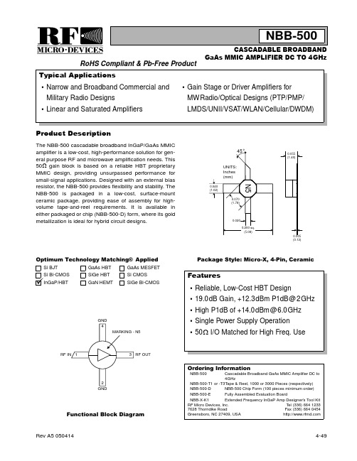
NBB-500
Pin Function Description
Interface Schematic
1
RF IN
RF input pin. This pin is NOT internally DC blocked. A DC blocking capacitor,
suitable for the frequency of operation, should be used in most applica-
2 of 12 /
7628 Thorndike Road, Greensboro, NC 27409-9421 · For sales or technical support, contact RFMD at (+1) 336-678-5570 or sales-support@.
and connect immediately to ground plane.
3
RF OUT
RF output and bias pin. Biasing is accomplished with an external series
resistor and choke inductor to VCC. The resistor is selected to set the DC
200
°C
Operating Temperature
-45 to +85
°C
Storage Temperature
-65 to +150
°C
Exceeding any one or a combination of these limits may cause permanent damage.
Caution! ESD sensitive device.
/
1 of 12
NBB-500
Absolute Maximum Ratings
Parameter
Rating
Unit
RF Input Power
+20
dBm
Power Dissipation
300
mW
Device Current
70
mA
Channel Temperature
NBB-500Cascadable Broadband GaAs MMIC Amplifier DC to 4 GHz
NBB-500
CASCADABLE BROADBAND GaAs MMIC AMPLIFIER DC TO 4GHz
RoHS Compliant & Pb-Free Product Package Style: Micro-X, 4-Pin, Ceramic
current into this pin to a desired level. The resistor value is determined by
the following equation:
R = (---V----C---C-----–----V----D----E---V---I--C----E----)
tions. DC coupling of the input is not allowed, because this will override the
internal feedback loop and cause temperature instability.
2
GND
Ground connection. For best performance, keep traces physically short
12.3 14.0
Байду номын сангаас
3.2 +26.5
-17.0
3.6
3.9
4.2
-0.0015
Unit
dB dB dB dB
GHz
dBm dBm dB dBm dB
V dB/°C
Condition
VD=+3.9V, ICC=35mA, Z0=50Ω, TA=+25°C f=0.1GHz to 1.0GHz f=1.0GHz to 2.0GHz f=2.0GHz to 4.0GHz f=0.1GHz to 3.0GHz f=0.1GHz to 4.0GHz f=4.0GHz to 6.0GHz f=6.0GHz to 10.0GHz BW3 (3dB)
RoHS status based on EUDirective2002/95/EC (at time of this document revision).
Parameter
Overall
Small Signal Power Gain, S21
Gain Flatness, GF Input and Output VSWR
Applications
Narrow and Broadband Commercial and Military Radio Designs
Linear and Saturated Amplifiers
Gain Stage or Driver Amplifiers for MWRadio/Optical Designs (PTP/PMP/ LMDS/UNII/VSAT/WLAN/Cellular/DWDM)
Features
Reliable, Low-Cost HBT Design
19.0dB Gain, +12.3dBm P1dB @ 2 GHz
High P1dB of +14.0 dBm @ 6.0 GHz
Single Power Supply Operation
50Ω I/O Matched for High Freq. Use
Rev A9 DS070327
7628 Thorndike Road, Greensboro, NC 27409-9421 · For sales or technical support, contact RFMD at (+1) 336-678-5570 or sales-support@.
Optimum Technology Matching® Applied
GaAs HBT
9GaAs MESFET InGaP HBT
SiGe BiCMOS Si BiCMOS SiGe HBT
GaAs pHEMT Si CMOS Si BJT
GaN HEMT
RF MICRO DEVICES®, RFMD®, Optimum Technology Matching®, Enabling Wireless Connectivity™, PowerStar®, POLARIS™ TOTAL RADIO™ and UltimateBlue™ are trademarks of RFMD, LLC. BLUETOOTH is a trademark owned by Bluetooth SIG, Inc., U.S.A. and licensed for use by RFMD. All other trade names, trademarks and registered trademarks are the property of their respective owners. ©2006, RF Micro Devices, Inc.
RF IN 1
GND 4
MARKING - N5
3 RF OUT
2 GND
Functional Block Diagram
Product Description
The NBB-500 cascadable broadband InGaP/GaAs MMIC amplifier is a low-cost, high-performance solution for general purpose RF and microwave amplification needs. This 50Ω gain block is based on a reliable HBT proprietary MMIC design, providing unsurpassed performance for smallsignal applications. Designed with an external bias resistor, the NBB-500 provides flexibility and stability. The NBB-500 is packaged in a low-cost, surface-mount ceramic package, providing ease of assembly for high-volume tape-and-reel requirements. It is available in either packaged or chip (NBB-500-D) form, where its gold metallization is ideal for hybrid circuit designs.
The information in this publication is believed to be accurate and reliable. However, no responsibility is assumed by RF Micro Devices, Inc. ("RFMD") for its use, nor for any infringement of patents, or other rights of third parties, resulting from its use. No license is granted by implication or otherwise under any patent or patent rights of RFMD. RFMD reserves the right to change component circuitry, recommended application circuitry and specifications at any time without prior notice.