MIT-IC lab testing
材料类实验室名称翻译
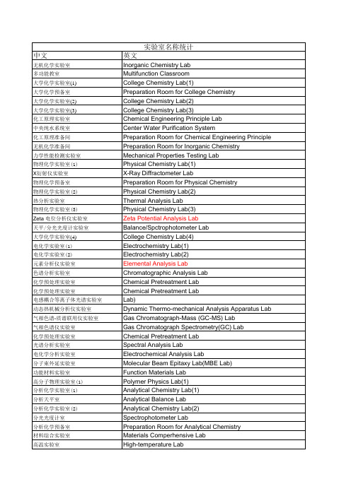
实验室名称统计 英文
Polymer Physics Lab Organic Chemistry Lab Fine Chemicals Lab Synthetic Chemistry Lab Polymer Chemistry Lab Preparation Room for Polymer Chemistry Preparation Room for Polymer Physics Composites Preparation Lab(1) Composites Preparation Lab(2) Composites Preparation Lab(3) Powder Technology Laboratory High-temperature Lab Basic Materials Lab Microscopes Lab Atomic Force Microscope Lab(AFM Lab)
中文
无机化学实验室 多功能教室 大学化学实验室(1) 大学化学预备室 大学化学实验室(2) 大学化学实验室(3) 化工原理实验室 中央纯水系统室 化工原理准备间 无机化学准备间 力学性能检测实验室 物理化学实验室(1) X衍射仪实验室 物理化学预备室 物理化学实验室(2) 热分析实验室 物理化学实验室(3) Zeta 电位分析仪实验室 天平/分光光度计实验室 大学化学实验室(4) 电化学实验室(1) 电化学实验室(2) 元素分析仪实验室 色谱分析实验室 化学预处理实验室 化学预处理实验室 电感耦合等离子体光谱实验室 动态热机械分析仪实验室 气相色谱-质谱联用仪实验室 气相色谱仪实验室 化学预处理实验室 光谱分析实验室 电化学分析实验室 分子束外延实验室 功能材料实验室 高分子物理实验室(1) 分析化学实验室(1) 分析天平室 分析化学实验室(2) 分光光度计室 分析化学预备室 材料综合实验室 高温实验室
实验室专业术语中英文翻译对照

实验室专业术语中英文翻译对照自动化实验室Automation Lab语言实验室Language Lab现代产品设计与制造技术实验室Modern Product Design & Manufacturing Tec hnology Lab计算机集成制造实验室Computer Integrated Manufac turing Sy stem Lab先进设计技术实验室Adv anced Design Tec hnology Lab机械设计基础实验室Machine Design Lab包装工程实验室Pac k ing Engineering Lab机械制造技术实验室Machine Manufacturing Lab精密机械测量技术实验室Precise Mac hine M easuring Tec hnology Lab数控技术与传动控制实验室NC Technol ogy & Trans mission C ontrol Lab设计创新实验室Innov ati on & Practic e Lab机械CAD中心Mechanic al CAD Center工作设计与时间研究实验室Job Design & Time Study Lab企业资源规划实验室Enterprise Resource Planning Lab系统仿真与设施规划实验室Sy s tem Si mulation & Facility Layout Lab人因工程实验室Human Fac tors & Ergonomics Lab液压与气动实验室Hy draulic & Pneumatic Lab汽车性能和结构实验室Auto Performanc e & C onstruc tion Lab发动机性能实验室Engine Perfor mance Lab汽车电子电气实验室Auto Elec tronic & Electric Lab数字媒体技术实验室Digital Media Technolog y Lab数字媒体技术基础实验分室Digital Media Technolog y Foundati on Lab数字影视实验分室Digital TV & Film Lab计算机动画与虚拟现实实验室Computer Animation & Virtual Reality Lab先进控制技术实验室Adv anced Control Tec hnology Lab楼宇智能化实验分室Intelligent Buildi ng Lab智能测控实验分室Intelligent Meas urement & Control Technolog y Lab运动控制与图象识别系统实验分室Motion C ontrol & Image R ecognition Sy stem Lab控制网络实验分室Control Network Lab自动控制系统实验分室Automatic Control System Lab自动控制原理实验分室Automatic Control Principl e Lab自动化学科创新实验室Automation Subject Innovation Lab电力电子技术分室Power El ectronics Technolog y Lab计算机控制技术实验分室Computer Control Technolog y Lab高压实验室High Voltage Technolog y Lab电机与控制实验室Electrical Machi ner y & C ontrol Lab电路与系统实验室Circuitry & Sy stem LabIC设计实验室IC Design LabESDA 与嵌入式技术实验室ESDA & Embedded Technolog y Lab微机原理实验室Microcomputer Principle Lab电力系统继电保护实验室Power Sy s tem Relay Protection Lab供配电技术实验室Power Supply Lab电力系统仿真实验室Power Sy s tem Emul ation Lab基础化学实验室Basic Chemistr y Lab无机化学分室Inorganic Chemistry Lab有机化学分室Organic Chemistry Lab基础分析化学分室Basic Analytical Chemistr y Lab物理化学分室Phy sical Chemistr y Lab综合仪器实验室Instrumental Lab化工原理实验室Chemic al Engineering Principle Lab化学工程与工艺实验室Chemic al Engineering & Tec hnology Lab食品科学与工程实验室Food Science & Engineering Lab生物工程实验室Biological Engineering Lab应用化学实验室Applied Chemistr y Lab制药工程实验室Phar mac y Engineering Lab清洁化学技术实验室Clean Chemical Tec hnol ogy Lab电动汽车研究实验室Electro-Motion Auto Res earch Lab电动汽车驱动性能检测分室Electro-Motion Auto Perfor manc e Tes t Lab现代信息技术实验室Modern Information Technol ogy Lab宽带及视频通信分室ADSL & Video Communic ation LabSDH技术分室SDH Technology Lab虚拟测试技术分室Virtual Test Technolog y Lab网络测控与光机电一体化分室Network Control & Electromec hanical Lab光电信息分室Photo-Electricity Infor mati on Technolog y Lab网络多媒体技术分室Network Multimedia Technolog y Lab生物特征图像识别技术分室Bio- Charac ter Image R ecognition Tec hnol ogy Lab EDA与DSP技术分室EDA & DSP Technolog y Lab现代通信技术实验室Modern C ommunicati on Technolog y Lab通信原理分室Communic ation Principl e Lab现代交换技术分室Modern Switch Tec hnolog y Lab无线通信分室Wireless Communic ation Tec hnol ogy Lab光纤通信分室Optic-Fiber Communic ation Lab移动通信分室Mobile Communic ation Lab网络通信与软件分室Network & Software Lab应用电子技术实验室Applied El ectronic Technolog y Lab信号与系统实验室Signal & Sy s tem Lab数字电视实验室Digital TV Lab微机测控技术实验室Microcomputer Measurement & Control Tec hnology Lab单片微机与嵌入式系统实验室Single Chip-Microcomputer & Embedded Sy stem Lab 动态测试与控制实验室Dy namic Test & Control Lab传感器与检测技术实验室Sens or & Measurement Technolog y Lab精密仪器与光电工程实验室Precise Instrument & Optoel ectronic Engineering Lab信息技术基础实验室IT Foundation Lab高频技术实验室High Frequenc y Tec hnol ogy Lab道路与桥梁工程实验室Highway & Bridge Engineering Lab给水排水工程实验室Water Suppl y & Was te Water Lab土木工程材料实验室Civ il Engineering Materials Lab唯雅诺自动化网建筑设备工程实验室Building Equipment Lab建筑学实验室Architectural Lab交通运输工程实验室Communic ation & Trans portation Lab结构工程实验室Structural Engineering Lab控制测量实验室Control Sur v ey Lab力学实验室Mechanics Lab流体力学实验室Hy drody namics Lab"S"技术实验室S Technolog y Lab岩土工程实验室Geotechnical Engineering Lab城市规划实验室Urban Pl anning Lab工程管理模拟实验室Engineering Management Si mulating Lab电子商务专业实验室Electronic C ommerc e Lab企业管理实验室Enter prise Management Lab地理信息系统实验室Geographic Information Sy stem Lab信息系统基础实验室Infor mati on Sy stems Lab会计手工模拟实验室Hand Acc ounting Imitati v e Lab计算机体系结构实验室Computer Architectures & Organization Lab计算机组成原理分室Computer Organization Lab接口与通讯分室Interface & Communic ation Lab智能工程分室Intelligent Engineering Lab微处理器设计分室Microprocessor Design Lab计算机软件工程实验室Computer Software Engineering Lab软件分室Computer Software Lab.图象处理和图形学分室Image Processi ng & Computer Gr aphics Lab网络安全分室Network Sec urity Lab软件项目管理分室Softwar e Projec t Management Lab现代计算机技术实验室Modern C omputer Tec hnol ogy LabSUN工作站分室SUN Wor k Station Lab计算机网络工程分室Computer Networ k Engineering Lab材料与能源学院热处理实验室Heat Treatment Lab金属腐蚀与防护实验室Metal Corrosion & Protec tion Lab金相显微镜实验室Metallographical Microscope Lab物理性能实验室Phy sical Pr operty Lab高分子材料制备实验室Pol y mer Materials Preparation Lab高分子材料结构与性能实验室Pol y mer Materials Str ucture & Properties Lab 高分子材料成型实验室Pol y mer Materials Processing Lab热工基础实验室Basic Ther mal Engineering Lab制冷与空调实验室Air Conditioning & R efrigeration Lab集成电路工艺实验室IC Process Lab电子元器件测试实验室Electronic D ev ice Measurement Lab电子薄膜材料实验室Electronic Fil m Materials Lab材料成型及控制实验室Material Proc essing & Control Lab模具技术实验室Die & Moul d Tec hnology Lab功能材料的制备与应用技术实验室非晶态材料分室Amor phous Materials Lab表面工程分室Surfac e Engineering Lab热型连铸分室Heated Mold Continuous C asting Lab储能材料分室Energy Storage M aterials Lab先进材料结构与性能分室Adv anced Materials Structure & Properties Lab 环境工程实验室Env ironmental Engineering Lab水污染控制工程分室Water Polluti on Control Lab大气污染控制工程分室Air Pollution Control Lab固体废物处理工程分室Solid Waste Treatment Lab噪声污染控制工程分室Noise Pollution Control Lab环境监测分室Env ironment Monitoring Lab环境科学实验室Env ironmental Scienc e Lab环境信息分室Env ironmental Information Sy stem Lab环境化学分室Env ironmental C hemistry Lab环境生物实验室Env ironmental Biolog y Lab大型精密仪器室Exactitude Apparatuses Room信息与计算科学实验室Infor mati on & Computati on Scienc e Lab光电技术实验室Optoelectronic Tec hnology Lab光信息技术实验室Technolog y of Optical Information Lab微电子技术实验室Microelectronic Tec hnology Lab电子技术综合实验室Electronic Technolog y Lab工业设计实验室Industrial Design Lab服装设计与工程实验室Apparel Design Lab基础造型实验室Fundamental Design Lab摄影分室Photography Lab陶艺设计与制作分室Pottery Design & F acture Lab环境艺术设计实验室Env ironment Design Lab视觉传达设计实验室Visual Communic ation Design Lab家具设计实验室Furniture D ecorati on Lab模拟法庭Mock Trial Room数码钢琴室Digital Piano Room社会工作实验室Social Wor k Lab工程训练实验教学示范中心Engineering Training Demons tration Center 铸造实习室Casting铣刨磨实习室Milling/ Planer/Grinder数控加工实习室CNC Machining数控编程实习室Programmi ng普通车床实习室Turning Lathe焊接实习室Welding钳工实习室Benc h Work热处理/金相分析实习室Heat Treatment & Microstructure压力加工实习室Forging测量实习室Measurement唯雅诺自动化网大学物理基础实验室College Phy sics F oundation Lab大学物理综合实验室College Phy sics Sy nthesized Lab电工电子实验中心Electrical & Electronic Ex perimental C enter电工基础实验室Electronic F oundation Lab电子技术实验室Electrical Technol ogy Lab电工与电子技术实训室Electrical & Electronic Training计算机基础实验中心Computer Ex perimental Center计算机基础实验室Computer Foundation Lab计算机组装实验室Computer Assembling Lab计算机组网实验室Computer Networ k Lab实验仪器名称中英文对照表仪器中文名称仪器英文名称英文缩写原子发射光谱仪Atomic Emission Spectrometer AES电感偶合等离子体发射光谱仪Inducti v e C oupl ed Plas ma Emission Spectrometer ICP直流等离子体发射光谱仪 Direct Current Pl asma Emission Spec trometer DCP紫外-可见光分光光度计 UV-Visible Spec trophotometer UV-Vis微波等离子体光谱仪 Microwave Induc tive Pl asma Emission Spectrometer MIP原子吸收光谱仪Atomic Absorption Spec troscopy AAS原子荧光光谱仪Atomic Fluoresc enc e Spectroscopy AF S傅里叶变换红外光谱仪FT-IR Spectrometer FTIR傅里叶变换拉曼光谱仪FT-Raman Spectrometer FTIR-Raman气相色谱仪 Gas Chromatograph GC高压/效液相色谱仪High Pressure/Performance Liquid Chr omatography HPLC离子色谱仪 Ion Chromatograph凝胶渗透色谱仪Gel Per meation Chromatograph GPC体积排阻色谱 Size Ex cl usion Chromatograph SECX射线荧光光谱仪 X-Ray Fluoresc enc e Spectrometer XRFX射线衍射仪X-Ray Diffractomer XRD同位素X荧光光谱仪Isotope X-Ray Fluoresc enc e Spectrometer电子能谱仪 Elec tron Energy Disperse Spectroscopy能谱仪 Energ y Disperse Spec troscopy ED S质谱仪 Mass Spec trometer MSICP-质谱联用仪ICP-MS IC P-MS 气相色谱-质谱联用仪 GC-MS GC-MS 液相色谱-质谱联用仪 LC-MS LC-MS 核磁共振波谱仪Nuclear Magnetic R esonanc e Spectrometer NMR电子顺磁共振波谱仪 Electron Paramagnetic Resonance Spectrometer ESR极谱仪 Polarograph伏安仪 Voltammerter自动滴定仪 Automatic Titrator电导仪 Conducti v ity MeterpH计 pH Meter水质分析仪 Water Tes t Kits电子显微镜 Elec tro Microscopy光学显微镜 Optical Microscopy金相显微镜 Metallurgical Microscopy扫描探针显微镜Sc anning Probe Microscopy表面分析仪 Surface Anal y z er无损检测仪 Ins trument for N ondestructi ve Testi ng物性分析Phy sical Property Anal y sis热分析仪Thermal Anal y zer粘度计 Visc ometer流变仪 Rheometer粒度分析仪 Particle Size Anal y zer热物理性能测定仪 Ther mal Phy sical Property Tester电性能测定仪 Electrical Property Tester光学性能测定仪Optical Property Tester机械性能测定仪Mechanic al Property Tes ter燃烧性能测定仪Combustion Property Tester老化性能测定仪Aging Property Tes ter生物技术分析 Biochemic al anal y sisPCR仪Instrument for Pol ymeras e Chain R eaction PCR DNA及蛋白质的测序和合成仪 Sequencers and Synthesizers for DNA and Protein传感器 Sens ors其他 Other/Miscellaneous流动分析与过程分析 Fl ow Anal y tic al and Pr ocess Anal y tical C hemistry气体分析Gas Anal y sis基本物理量测定Basic Phy sics样品处理Sample Handling金属/材料元素分析仪 Metal/material el emental anal y sis环境成分分析仪CHN Anal y sis发酵罐 F ermenter生物反应器 Bio-reactor摇床 Shak er离心机 Centrifuge超声破碎仪 Ultrasonic Cell Disruptor超低温冰箱 Ultra-low Temper ature Freezer恒温循环泵 Cons tant Temperature Circulator超滤器 Ultrahigh Purity Filter冻干机 Freeze Dr y ing Equipment部分收集器 Fraction Collector氨基酸测序仪 Protei n Sequenc er氨基酸组成分析仪 Ami no Acid Anal y z er多肽合成仪 Peptide s ynthesizerDNA测序仪 DNA SequencersDNA合成仪 DNA synthesizer紫外观察灯 Ultrav iolet Lamp唯雅诺自动化网化学发光仪 Chemiluminesc enc e Apparatus紫外检测仪 Ultrav iolet Detec tor电泳 Electr ophoresis酶标仪 ELIASACO2培养箱 CO2 Incubators倒置显微镜 Inverted Microscope超净工作台 Bechtop流式细胞仪 Flow C y tometer微生物自动分析系统 Automatic Analy z er for Microbes生化分析仪 Bioc hemical Anal y zer血气分析仪 Blood-gas Anal y zer电解质分析仪 Electrol y tic Anal y zer尿液分析仪 Urine Anal y zer临床药物浓度仪Anal y zer for Clinic Medicine Conc entration 血球计数器 Hematoc y te Counter实验室家具laborator y/lab fur niture威盛亚wilsonart台面countertop/wor k top实验台laborator y cas ewor k/cabinet中央台island bench边台wall benc h试剂架reagent s helf/rac k天平台balance tabl e仪器台instrument table通风系统v entilati on s y s tem通风柜/橱fume hood/c upboard药品柜medical (storage) c abinet/c upboard器皿柜v ess el cabinet气瓶柜gas cy linder (storage) c abinet实验凳laborator y/lab stool实验椅lab chair配件accessories。
麻省理工学院微电子实验室简介
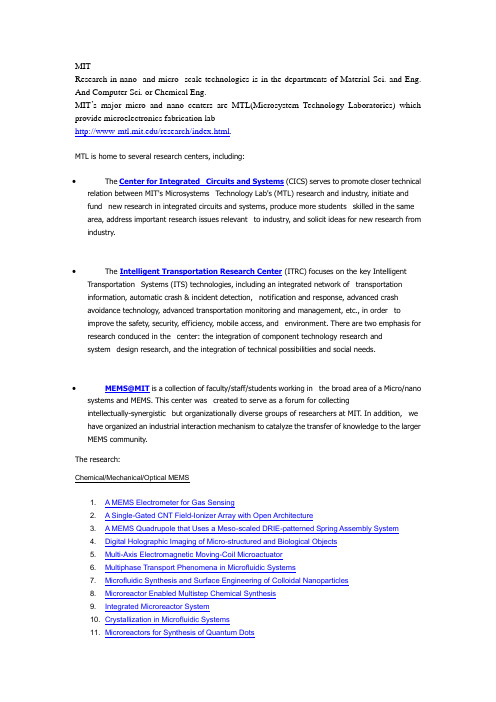
MITResearch in nano- and micro- scale technologies is in the departments of Material Sci. and Eng. And Computer Sci. or Chemical Eng.MIT’s major micro and nano centers are MTL(Microsystem Technology Laboratories) which provide microelectronics fabrication lab/research/index.html.MTL is home to several research centers, including:∙The Center for Integrated Circuits and Systems (CICS) serves to promote closer technical relation between MIT's Microsystems Technology Lab's (MTL) research and industry, initiate and fund new research in integrated circuits and systems, produce more students skilled in the same area, address important research issues relevant to industry, and solicit ideas for new research from industry.∙The Intelligent Transportation Research Center (ITRC) focuses on the key Intelligent Transportation Systems (ITS) technologies, including an integrated network of transportation information, automatic crash & incident detection, notification and response, advanced crashavoidance technology, advanced transportation monitoring and management, etc., in order toimprove the safety, security, efficiency, mobile access, and environment. There are two emphasis for research conduced in the center: the integration of component technology research andsystem design research, and the integration of technical possibilities and social needs.∙MEMS@MIT is a collection of faculty/staff/students working in the broad area of a Micro/nano systems and MEMS. This center was created to serve as a forum for collectingintellectually-synergistic but organizationally diverse groups of researchers at MIT. In addition, we have organized an industrial interaction mechanism to catalyze the transfer of knowledge to the larger MEMS community.The research:Chemical/Mechanical/Optical MEMS1. A MEMS Electrometer for Gas Sensing2. A Single-Gated CNT Field-Ionizer Array with Open Architecture3. A MEMS Quadrupole that Uses a Meso-scaled DRIE-patterned Spring Assembly System4. Digital Holographic Imaging of Micro-structured and Biological Objects5. Multi-Axis Electromagnetic Moving-Coil Microactuator6. Multiphase Transport Phenomena in Microfluidic Systems7. Microfluidic Synthesis and Surface Engineering of Colloidal Nanoparticles8. Microreactor Enabled Multistep Chemical Synthesis9. Integrated Microreactor System10. Crystallization in Microfluidic Systems11. Microreactors for Synthesis of Quantum Dots12. A Large Strain, Arrayable Piezoelectric Microcellular Actuator13. MEMS Pressure-sensor Arrays for Passive Underwater Navigation14. A Low Contact Resistance MEMS-Relay15. "Fast Three-Dimensional Electrokinetic Pumps for Microfluidics16. Carbon Nanotube - CMOS Chemical Sensor Integration17. An Energy Efficient Transceiver for Wireless Micro-Sensor Applications18. Combinatorial Sensing Arrays of Phthalocyanine-based Field-effect Transistors19. Nanoelectromechanical Switches and Memories20. Integrated Carbon Nanotube Sensors21. Organic Photovoltaics with External Antennas22. Integrated Optical-wavelength-dependent Switching and Tuning by Use of Titanium Nitride (TiN)MEMS Technology23. Four Dimensional Volume Holographic Imaging with Natural Illumination24. White Light QD-LEDs25. Organic Optoelectronic Devices Printed by the Molecular Jet Printe26. Design and Measurement of Thermo-optics on SiliconBioMEMS1. A Microfabricated Platform for Investigating Multicellular Organization in 3-D Microenvironments2. Microfluidic Hepatocyte Bioreactor3. Micromechanical Control of Cell-Cell Interaction4. A MEMS Drug Delivery Device for the Prevention of Hemorrhagic Shock5. Multiwell Cell Culture Plate Format with Integrated Microfluidic Perfusion System6. Characterization of Nanofilter Arrays for Biomolecule Separation7. Patterned Periodic Potential-energy Landscape for Fast Continuous-flow BiomoleculeSeparation8. Continuous-flow pI-based Sorting of Proteins and Peptides in a Microfluidic Chip Using DiffusionPotential9. Cell Stimulation, Lysis, and Separation in Microdevices10. Polymer-based Microbioreactors for High Throughput Bioprocessing11. Micro-fluidic Bioreactors for Studying Cell-Matrix Interactions12. A Nanoscanning Platform for Biological Assays13. Label-free Microelectronic PCR Quantification14. Vacuum-Packaged Suspended Microchannel Resonant Mass Sensor for BiomolecularDetection15. Microbial Growth in Parallel Integrated Bioreactor Arrays16. BioMEMS for Control of the Stem-cell Microenvironment17. Microfluidic/Dielectrophoretic Approaches to Selective Microorganism Concentration18. Microfabricated Approaches for Sorting Cells Using Complex Phenotypes19. A Continuous, Conductivity-Specific Micro-organism Separator20. Polymer Waveguides for Integrated BiosensorsEnabling Technology1. A Double-gated CNF Tip Array for Electron-impact Ionization and Field Ionization2. A Double-gated Silicon Tip, Electron-Impact Ionization Array3. A Single-Gated CNT Field-Ionizer Array with Open Architecture4. Aligning and Latching Nano-structured Membranes in 3D Micro-Structures5. Characterization and Modeling of Non-uniformities in DRIE6. Understanding Uniformity and Manufacturability in MEMS Embossing7. Atomic Force Microscopy with Inherent Disturbance Suppression for Nanostructure Imaging8. Vacuum-Sealing Technologies for Micro-chemical Reactors9. Direct Patterning of Organic Materials and Metals Using Micromachined Printheads10. MEMS Vacuum Pump11. Rapid and Shape-Controlled Growth of Aligned Carbon Nanotube Structures12. Prediction of Variation in Advanced Process Technology Nodes13. Parameterized Model Order Reduction of Nonlinear Circuits and MEMS14. Development of Specialized Basis Functions and Efficient Substrate Integration Techniques forElectromagnetic Analysis of Interconnect and RF Inductors15. A Quasi-convex Optimization Approach to Parameterized Model-order Reduction16. Amorphous Zinc-Oxide-Based Thin-film Transistors17. Magnetic Rings for Memory and Logic Devices18. Studies of Field Ionization Using PECVD-grown CNT Tips19. Growth of Carbon Nanotubes for Use in Origami Supercapacitors20. Self-Alignment of Folded, Thin-Membranes via Nanomagnet Attractive Forces21. Control System Design for the Nanostructured Origami™ 3D Nanofabrication Process22. Measuring Thermal and Thermoelectric Properties of Single Nanowires and Carbon Nanotubes23. Nanocomposites as Thermoelectric Materials24. CNT Assembly by Nanopelleting25. Templated Assembly by Selective Removal26. Building Three-dimensional Nanostructures via Membrane FoldingPower MEMS1. Hand-assembly of an Electrospray Thruster Electrode Using Microfabricated Clips2. A Fully Microfabricated Planar Array of Electrospray Ridge Emitters for Space PropulsionApplications3. Thermal Management in Devices for Portable Hydrogen Generation4. Autothermal Catalytic Micromembrane Devices for Portable High-Purity Hydrogen Generation5. Self-powered Wireless Monitoring System Using MEMS Piezoelectric Micro Power Generator6. An Integrated Multiwatt Permanent Magnet Turbine Generator7. Micro-scale Singlet Oxygen Generator for MEMS-based COIL Lasers8. A Thermophotovoltaic (TPV) MEMS Power Generator9. MEMS Vibration Harvesting for Wireless Sensors10. Fabrication and Structural Design of Ultra-thin MEMS Solid Oxide Fuel Cells11. Tomographic Interferometry for Detection of Nafion® Membrane Degradation in PEM Fuel Cells∙The Center for Integrated Photonic Systems (CIPS) mission is to create a meaningful vision of the future, a framework for understanding how technology, industry and business interact and evolve together in the future is required. Models provide us with a process for analyzing the many complex factors that shape this industry and the progress of related technologies.The materials processing center .Making matter meet human needsResearchThe Center brings together MIT faculty and research staff from diverse specialties to collaborate on interdisciplinary materials problems. Center research involves over 150 faculty, research staff, visiting scientists, and graduate and undergraduate students.MPC researchers cover the full range of advanced materials, processes, and technologies, including∙electronic materials∙batteries & fuel cells∙polymers∙advanced ceramics∙materials joining∙composites of all types∙photonics∙electrochemical processing ∙traditional metallurgy∙environmental degradation∙materials modeling- many scale ∙materials systems analysis∙nanostructured materials∙magnetic materials and processes ∙biomaterials∙materials economicsFaculty ProfilesA.I. AkinwandeFlat panel displays,Vacuum Microelectronics and its application to flat panel displays, RF power sources, and sensors. Wide bandgap semiconductors and applications to flat panel displays, UV emitters and RF power sourcesView current research abstracts (pdf)G. BarbastathisBiomedical design instrumentation; precision engineering robotics; volume holographic architectures for data storage, color-selective tomographic imaging, and super-resolving confocal microscopy; interferometric surface characterization; and adaptive micro-opto-mechanics. Optical MEMS.View current research abstracts (pdf)View group web siteM. BazantResearch focuses on transport phenomena in materials and engineering systems, especially diffusion coupled to fluid flow. My group is currently studying granular flow in pebble-bed nuclear reactors, nonlinear electrokinetic flows in microfludic devices, ion transport in thin-film lithium batteries, and advection-diffusion-limited aggregation.View current research abstracts (pdf)View group web siteS. BhatiaResearch focuses on applications of micro- and nanotechnology to tissue repair and regeneration. Emphasis on development of microfabrication tools to improve cellular therapies for liver disease, living cell arrays to study stem cell biology, and nanoparticles for cancer diagnosis and treatment.View current research abstracts (pdf)View group web siteD. BoningSemiconductor manufacturing. Modeling and control of chemical mechanical polishing. Variation modeling and reduction in fabrication processes, devices, and interconnects. Run by run and feedback control for quality and environment in semiconductor fabrication. Software systems for distributed and collaborative computer aided design and fabrication.View current research abstracts (pdf)View group web siteA.P. ChandrakasanDesign of digital integrated circuits and systems. Emphasis on the energy efficient implementation of distributed microsensor and signal processing systems. Protocols and Algorithms for Wireless Systems. Circuits techniques for deep sub-micron technologies.View current research abstracts (pdf)View group web siteG. ChenMicro- and nanoscale heat transfer and energy conversion with applications in thermoelectrics, photonics, and microelectronics; nano-mechanical devices and micro-electro-mechanical systems; radiation and electromagnetic metamaterials.View current research abstracts (pdf)View group web siteM. CulpepperResearch focuses on precision interfaces, precision manufacturing, design for manufacturing, applying precision principles as enabling technologies in multi-disciplinary product design: electronic test equipment, automotive systems, precision compliant mechanisms.View current research abstracts (pdf)View group web siteL. DanielResearch focuses on engineering design applications to drive research in simulation and optimization algorithms and software, design of microfabricated inductors.View current research abstracts (pdf)View group web siteP. DoyleUnderstanding the dynamics of single polymers and biomolecules under forces and fields; lab-on-chip separations, polymer rheology. DNA electrophoresis in microdevices. Superparamagnetic colloids. Brownian Dynamics simulations of complex molecules. Microheology of biopolymers.View current research abstracts (pdf)View group web siteA. EpsteinSmart engines, turbine heat transfer and aerodynamics, advanced diagnostic instrumentation, turbomachinery noise, environmental impact of aircraft.View current research abstracts (pdf)View group web siteD. FreemanBiological micromechanics, MEMS, light microscopy and computer microvision.View current research abstracts (pdf)牋牋牋牋牋牋牋牋牋牋牋?牋View group web siteM. GrayMicrofabricated devices for use in diagnostic medicine and biological research. Particle and fuid analysis of flowing media using absorbance and fluorescence techniques as a means for understanding cell or organism metabolism and phenotypic expression.View group web siteJ. HanBioMEMS, biomolecule analysis, micro/nanofluidics, micro-analysis systems.View current research abstracts (pdf)View group web siteJ. JacobsonDevelopment of processes for directly and continuously printing communication, computation, and displays onto arbitrary substrates. Electronic control of biomolecules.View group web siteK. JensenMicrofabrication and characterization of devices and systems for chemical synthesis and detection, hydrocarbon fuel conversion to electrical energy, bioprocessing and bioanalytics. Multiscale simulation of transport and reaction processes. Chemical vapor deposition of polymer, metal, and semiconductor thin films. Synthesis and characterization of quantum dot composite materials.View current research abstracts (pdf)View group web siteR. KarnikMicro- and nanofluidic systems. Application of transport phenomena in nanofluidics for flow control, separation, sensing. Microfluidic devices for studying chemical kinetics and nanoparticle synthesis.View group web siteS.G. KimSystems Design and Manufacturing, MEMS for optical beam steering, microphotonic packaging and active alignment, micro power generation, massive parallel positional assembly of nanostructures, and nano actuator array.View current research abstracts (pdf)View group web siteJ.H. LangAnalysis, design and control of electromechanical systems. Application to traditional electromagnetic actuators, micron scale actuators and sensors, and flexible structures.View current research abstracts (pdf)View group web siteC. LivermoreMicroElectroMechanical Systems (MEMS). Design and fabrication of high power microsystems. Nanoscale self-assembly and manufacturing.View current research abstracts (pdf)View group web siteS. ManalisApplication of micro- and nanofabrication technologies towards the development of novel methods for probing biological systems. Current projects focus on electrical and mechanical detection schemes for analyzing DNA, proteins, and cells.View current research abstracts (pdf)View group web siteD.J. PerreaultAnalysis, design, and control of cellular power converter architectures. DC/DC Converters fordual-voltage electrical systems. Electrical system transient investigation. Exploration of non-conventional electricity sources for motor vehicles.View group web siteM.A. SchmidtMicroElectroMechanical Systems (MEMS). Microfabrication technologies for integrated circuits, sensors, and actuators. Design of microsensor and microactuator systems.View current research abstracts (pdf)A. SlocumPrecision Engineering; Machine Design; Product Design.View current research abstracts (pdf)View group web siteC.V. ThompsonProcessing, structure, properties, performance, and reliability of thin films and structures for micro- and nano-devices and systems. Reliability and Interconnect.View current research abstracts (pdf)View group web siteT. ThorsenIntegrating microfluidic design and fabrication techniques, electronics and optics with biochemical applications. Optimizing channel dimensions, geometry, and layout to generate 3-D fluidic networks that are functional and scalable. Interface development to combine microfluidic technologies with pneumatic valves, MEMS-based detector systems, and software-based data acquisition and interpretation, creating devices for fundamental research and diagnostic applications.View current research abstracts (pdf)View group web siteH.L. TullerCharacterize and understand key electronic, microstructural, and optical properties of advanced ceramic materials. Fabrication andcharacterization of crystals, ceramics and glasses for electronic devices, lasers, electrochemical energy conversion, sensors and actuators.View current research abstracts (pdf)View group web siteJ. VoldmanBiological applications of microsystem technology. Engineering and use of microsystems for analysis and engineering of single cells. Physical and electrical cell manipulation. Design, modeling, microfabrication, and testing of microfluidic biological devices employing unconventional materials and fabrication processes. Electromechanics at the microscale.View current research abstracts (pdf)View group web siteE. N. WangDevelopment of MEMS/NEMS for: Biochemical sensing and detection; Thermal management of high power density and high performance systems; Diagnostics for biological systems and bio-functionality View group web siteB. WardlePower MEMS microyhydraulics, structural health monitoring, nanocomposites, damageresistance/tolerance of advanced composite materials, cost modeling in the structural design process, conversion of technology to value.View current research abstracts (pdf)View group web siteJ. WhiteTheoretical and practical aspects of numberical algorithms for problems in circuit, device, interconnect, packaging, and micromechanical system design; parallel numerical algorithms; interaction between numerical algorithms and computer architecture.View current research abstracts (pdf)View group web siteLaser-cooling brings large object near absolute zeroAnne Trafton, News OfficeApril 5, 2007Using a laser-cooling technique that could one day allow scientists to observe quantum behavior in large objects, MIT researchers have cooled a coin-sized object to within one degree of absolute zero.Fig.1Assistant professor Nergis Mavalvala, left, and Ph.D. student Thomas Corbitt are part of an international team that has devised a way to cool large objects to near absolute zero. Enlarge image (no JavaScript)Fig.Super-mirrorMIT researchers have developed a technique to cool this dime-sized mirror (small circle suspended in the center of large metal ring) to within one degree of absolute zero. Enlarge image (no JavaScript)Fig.2Assistant professor Nergis Mavalvala, right, and Ph.D. student Thomas Corbitt look over the laser system they use to cool a coin-sized mirror to within one degree of absolute zero. Enlarge image (no JavaScript)。
第三方医学检验实验室(ICL)行业研究报告
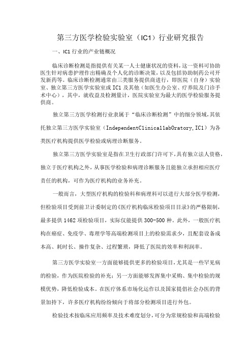
第三方医学检验实验室(IC1)行业研究报告一、IC1行业的产业链概况临床诊断检测是指提供有关某一人士健康状况的资料,这一资料可协助医生针对病患护理作出精确及个人化的诊断决策,以及包括协助制药公司开发新药等。
临床诊断检测通常由三类服务提供商进行,即医院(自身)实验室、独立第三方医学实验室或IC1及其他(如医生办公室、疗养院及门诊手术中心),其中,就收益及检测量计,医院实验室为最大的医学检验服务提供商。
独立第三方医学检测行业隶属于“临床诊断检测”中的细分领域,其依托独立第三方医学实验室(IndependentC1inica11abOratory,IC1)为各类医疗机构提供医学检验或病理诊断服务。
独立第三方医学实验室是指在卫生行政部门许可下,具有独立法人资格,独立于医疗机构之外,从事医学检验和病理诊断服务且能独立承担相应医疗责任的机构,可作为医疗机构的业务补充。
一般而言,大型医疗机构的检验科和病理科可以进行大部分医学检测,但检验项目受到前卫计委制定的《医疗机构临床检验项目目录》的严格限制,最多提供1462项检验项目,实际仅能提供300-500种。
此外,一般医疗机构在癌症、免疫学、毒理学等高端检测项目上的检验需求少,且配套设备成本高、耗时长、操作复杂、过程繁琐,降低了医院的效率和利润率。
第三方医学实验室一方面能够提供更多的检验项目,尤其是一些罕见病的检验,作为医院检验的补充;另一方面能够发挥集中采购、集中检验的规模优势,降低检验成本。
在医疗体系市场化运作以及国家提倡社会办医的背景加持下,许多医疗机构纷纷倾向于将部分检测项目进行外包。
检验技术按临床应用频率及技术难度划分,可分为常规检验和高端检验两类。
常规检验一般指2013年颁布的《医疗机构临床检验项目目录》之内的项目服务,主要包括血液检验、生化检验、免疫学检验等基础检验项目。
常规检验应用范围较广,无论在大型三甲医院还是基层医疗机构都有广泛的应用,但由于技术发展成熟,市场竞争激烈,利润较低。
100多个国家重点实验室的名称

100多个国家重点实验室的名称近年来,实验室在科研领域发挥着至关重要的作用。
各个国家都设立了不少重点实验室,致力于推动科技发展和创新。
本文将介绍一些世界各地的重点实验室,并对其名称进行概述。
美国:1. 麻省理工学院人工智能实验室(MIT AI Lab)- 专注于人工智能研究和技术创新。
2. 加州理工学院电子与计算机科学实验室(Caltech CSL)- 进行电子与计算机科学领域的前沿研究。
中国:1. 中国科学院计算数学与科学工程研究中心(CMSEC)- 科学计算与工程问题的研究与应用开发。
2. 清华大学先进技术研究院(THAT)- 开展先进技术研究和跨学科交叉研究。
英国:1. 牛津大学计算机科学实验室(Oxford Computer Science Lab)- 研究计算机科学及其应用领域的前沿问题。
2. 剑桥大学心理学研究实验室(Cambridge Psychology Research Lab)- 进行心理学研究,涵盖认知、社会和发展心理学等领域。
德国:1. 慕尼黑大学生理学与心理学实验室(Munich University Physiology and Psychology Lab)- 研究人体生理学和心理学相关问题。
2. 柏林工业大学机器人技术实验室(Berlin Institute of Technology Robotics Lab)- 研究机器人技术和自动化领域的创新技术。
日本:1. 东京大学材料科学实验室(University of Tokyo Materials Science Lab)- 研究材料科学和材料工程方面的问题。
2. 京都大学生命科学实验室(Kyoto University Life Science Lab)- 进行生命科学研究,包括生物学和生物医学等领域。
澳大利亚:1. 悉尼大学化学与生物分子科学实验室(University of Sydney Chemistry and Biomolecular Science Lab)- 进行化学和生物分子科学研究。
核酸适体筛选的国外课题组
核酸适体筛选的国外课题组
在核酸适体筛选领域,国外有许多知名的研究机构和实验室。
其中,美国麻省理工学院(MIT)的白建中实验室是该领域的先驱之一,在核酸适体的筛选和进化方面开展了多年的研究。
此外,1990年美国的Gold课题组和Szostak课题组通过基本相同的体外筛选技术,分别获得了能够与T4 DNA 聚合酶和小分子有机染料特异性结合的RNA序列。
Gold将该技术命名为“SELEX”,而Szostak将这种对靶标具有特异性结合能力的核酸命名为“aptamer(适配体)”。
以上内容仅供参考,建议查阅相关文献或咨询专业人士以获取更多信息。
集成电路测试工作流程英语小作文

集成电路测试工作流程英语小作文英文回答:Integrated circuit (IC) testing is a crucial step in ensuring the quality and reliability of electronic devices. It involves a systematic process to verify thefunctionality and performance of ICs before they are integrated into final products. Here's a breakdown of the typical workflow involved in IC testing:1. Test Planning and Strategy: Before testing begins,it's essential to develop a comprehensive test plan outlining the objectives, methodologies, and resources required for testing. This phase involves understanding the specifications of the ICs and defining the test coverage criteria. For example, if I'm testing a microcontroller,I'll need to consider factors like input/output functionality, clock speed, and power consumption.2. Test Development: Once the test plan is in place,the next step is to develop test programs or patterns that will be used to stimulate the IC and capture its responses. This involves writing code or using specialized software tools to generate test vectors. These vectors represent different input stimuli applied to the IC to evaluate its behavior under various conditions. For instance, if I'm testing a memory chip, I'll create test patterns to read and write data to different memory locations to check for any defects or inconsistencies.3. Test Execution: With test programs ready, it's time to execute them on the target ICs. This phase involves connecting the ICs to test equipment such as automated test equipment (ATE) or specific test fixtures. The ICs are subjected to the test patterns, and their responses are analyzed to determine whether they meet the expected specifications. During this stage, it's essential to monitor parameters like voltage, frequency, and temperature to ensure accurate testing. For example, if I'm testing a digital signal processor (DSP), I'll verify its computational accuracy by running mathematical algorithms and comparing the results against expected values.4. Data Analysis and Debugging: After completing the tests, the data collected needs to be analyzed to identify any deviations or failures. This involves comparing the actual test results with the expected outcomes specified in the test plan. If discrepancies are found, debugging techniques are employed to pinpoint the root cause of the issues. For instance, if I encounter failures in the output of an analog-to-digital converter (ADC), I'll investigate factors like noise, linearity, or calibration errors that could affect its performance.5. Reporting and Documentation: Finally, the results of the testing process are documented in detailed reports. These reports include summaries of the tests conducted, the outcomes obtained, any anomalies detected, and recommendations for further actions. Clear documentation is crucial for traceability and quality assurance purposes. Additionally, lessons learned from the testing process are recorded to improve future testing strategies and methodologies.In conclusion, the workflow for IC testing involves careful planning, meticulous execution, and thorough analysis to ensure the reliability and functionality of integrated circuits. By following a systematic approach and leveraging advanced testing techniques, manufacturers can deliver high-quality ICs that meet the demands of modern electronic devices.中文回答:集成电路(Integrated Circuit,IC)测试是确保电子设备质量和可靠性的关键步骤。
Best-testing -lab

Best-Testing-Lab E M S之九陰真經EMS密笈攻略本NEW 版一.名詞定義:1.感應線圈( induction coil ):外型形成一個迴圈的導體,當導體有電流流過會在其外殼平面產生磁場.2.短暫中斷(short interruption);電源供應消失一段時間不超過一分鐘.電源的中斷可以視為振幅100%的電壓下降.3.電壓變動(voltage variation):電源的電壓逐漸地變動到比額定電壓值高或低,變動的時間可以是長週期或短週期.4.耦合(coupling)(interaction between circuits transferring energy from one circuit to another)在電路間的交互作用,能量由一各電路轉換至另一個電路.5.耦合網路(coupling network);由一各電路到另一各,在所定義的阻抗轉換能量的電器電路.備考:耦合及去耦合網路裝置能被整合一各盒子.6.EFT/B:(Electrical fast transient/burst immunity test)電氣快速暫態/叢訊免疫力測試,電氣和電子設備在電源,信號和控制部分遇到重複電性快速暫態的性能.7. HCP:(Horizontal coupling plane):水平耦合面,用以模擬鄰近待測物的物體對待測物的靜電放電所使用的水平金屬面板;大小同測試桌。
8. VCP(Vertial coupling plane):垂直耦合面, 用以模擬鄰近待測物的物體對待測物的靜電放電所使用的垂直金屬面板.大小0.5m*0.5m.9. CDN(Coupling/Decoupling Network):耦合/去耦合網路.10.去耦合網路(decoupling networ,back filter):一電子電路用以避免磁場交互影響非待測設備.11.場強(field strength):場強僅適用於遠場的量測,此量測可以是電場或磁場的分量,也可以V/m,A/m或W/m²來表示,這些都可以彼此互相轉換.二.注意事項:ESD:EN61000-4-21.填寫ESD產生器之特性:Rc充電電阻:50 MΩ~ 100 MΩ.- Cs 儲能電容:____150_____ pF±_____10_____%-Rd 放電電阻:____330_____ Ω±_____10______%。
- 1、下载文档前请自行甄别文档内容的完整性,平台不提供额外的编辑、内容补充、找答案等附加服务。
- 2、"仅部分预览"的文档,不可在线预览部分如存在完整性等问题,可反馈申请退款(可完整预览的文档不适用该条件!)。
- 3、如文档侵犯您的权益,请联系客服反馈,我们会尽快为您处理(人工客服工作时间:9:00-18:30)。
Polysilicon
Fall 2005 – M.A. Schmidt
Single Crystal Silicon
Figure removed for copyright reasons.
Please see: Figure 3-5 in Pierret, Robert, and Gerold Neudeck. Modular Series on Solid State Devices. Reading, MA: Addison-Wesley, 1982. ISBN: 0201052873.
Please see: Kamins, T. Polysilicon for Integrated Circuit Application. Norwell, MA: Kluwer Academic Publishers, 1988.
T. Kamins Kluwer
Fall 2005 – M.A. Schmidt 3.155J/6.152J – Lecture 5 – Slide 16
MOS Capacitor
t
A
C = ε A/t = εrεo A/t C* = C / A εr (SiO2) = 3.9
Fall 2005 – M.A. Schmidt
εo = 8.85 x 10⁻¹⁴ F/cm
3.155J/6.152J – Lecture 5 – Slide 17
MOS Capacitance Measurement
RS = 4.53 Rave Rave = ½ (R’+R’’)
Fall 2005 – M.A. Schmidt
3.155J/6.152J – Lecture 5 – Slide 9
N Square Resistor
L = Lmask + ∆L
W = Wmask + ∆W
N = Lmask/Wmask >>1
Fall 2005 – M.A. Schmidt 3.155J/6.152J – Lecture 5 – Slide 25
MOS Capacitance Measurement
Three measurements Cox Cmin VFB Produce tox ND Qf CFB
Fall 2005 – M.A. Schmidt
R. Pierret
Fall 2005 – M.A. Schmidt 3.155J/6.152J – Lecture 5 – Slide 13
Single Crystal Silicon
Figure removed for copyright reasons.
Please see: Plummer, J., M. Deal, and P. Griffin. Silicon VLSI Technology: Fundamentals, Practice, and Modeling. Upper Saddle River, NJ: Prentice Hall, 2000. ISBN: 0130850373.
L = W
R = RS
Fall 2005 – M.A. Schmidt 3.155J/6.152J – Lecture 5 – Slide 5
Number of Squares
R = 2RS
R = RS/2
R = RS/3
R = 8RS
Fall 2005 – M.A. Schmidt
R = 6.5RS
T. Kamins Kluwer
Fall 2005 – M.A. Schmidt 3.155J/6.152J – Lecture 5 – Slide 15
Polysilicon Resistivity vs Dopant
Use for lab report
Figure removed for copyright reasons.
Resistivity Ω-cm
Fall 2005 – M.A. Schmidt
Process
Mask
3.155J/6.152J – Lecture 5 – Slide 4
Concept of Sheet Resistivity
R = ρ L/A = (ρ/t) (L/W)
Sheet Resistivity (RS) Ω/sq # of Squares
I I
+
V
-
Eliminates the effect of contact resistance
Fall 2005 – M.A. Schmidt
3.155J/6.152J – Lecture 5 – Slide 11
Analysis of Resistivity
Semiconductor Resistivity(ρ)/Conductivity(σ)
Plummer
Fall 2005 – M.A. Schmidt 3.155J/6.152J – Lecture 5 – Slide 14
Poly Resistivity vs Dep. Temp.
re removed for copyright reasons.
Please see: Kamins, T. Polysilicon for Integrated Circuit Application. Norwell, MA: Kluwer Academic Publishers, 1988.
Oxide
n-Si
C* = C / A
Fall 2005 – M.A. Schmidt 3.155J/6.152J – Lecture 5 – Slide 19
MOS Capacitor in Accumulation
+ + + + + + + +
-
C* = Cox = εox / tox
Fall 2005 – M.A. Schmidt 3.155J/6.152J – Lecture 5 – Slide 20
0.2 1
Fall 2005 – M.A. Schmidt
10
100
1000
R’/R’’
3.155J/6.152J – Lecture 5 – Slide 8
Van der Pauw
Implement a symmetric structure
R’ = R’’ f(R’/R’’) = 1
1/ρ = σ = q(µnn + µpp) n >> p σ = qµnn n=N (doping density) µSi = f(N) µpoly << µSi
3.155J/6.152J – Lecture 5 – Slide 12
N-type
Single Crystal Silicon
Fall 2005 – M.A. Schmidt
3.155J/6.152J – Lecture 5 – Slide 24
Effect of Oxide Charge
+ + + + + + + +
+ + + +
- - - - -
A net shift in C-V curve:
Need to add more negative charge (voltage) to invert surface
+ -
VGB vac
iac Ref: A. Akinwande
Fall 2005 – M.A. Schmidt
3.155J/6.152J – Lecture 5 – Slide 18
MOS Capacitor
Poly
tox
+ - + - + - + - + - + - + - + + - + - + - + - + - + - + - + + - + - + - + - + - + - + - + + - + - + - + + - + - + - + - + - + - + + - + - + - + - + - + - + + - + - + - + - + - + - + + - + - + - +
xs xs,max
Rapid VGB Change
Flatband VGB
VT Inversion
VFB
Depletion Accumulation
Cs = εSi / xs
Fall 2005 – M.A. Schmidt 3.155J/6.152J – Lecture 5 – Slide 23
C-V
R = RS (L/W) = RS [Lmask/(Wmask +∆W)]
Used to determine the process ‘bias’ (∆W)
Fall 2005 – M.A. Schmidt 3.155J/6.152J – Lecture 5 – Slide 10
4-Point Probe
3.155J/6.152J Lecture 5:
IC Lab Testing