KK74ACT02N中文资料
74HCT74N中文资料

元器件交易网
Philips Semiconductors
Product specification
Dual D-type flip-flop with set and reset; positive-edge trigger
FEATURES • Wide supply voltage range from 2.0 to 6.0 V • Symmetrical output impedance • High noise immunity • Low power dissipation • Balanced propagation delays • ESD protection: HBM EIA/JESD22-A114-A exceeds 2000 V MM EIA/JESD22-A115-A exceeds 200 V.
2003 Jul 10
2
元器件交易网
Philips Semiconductors
Product specification
Dual D-type flip-flop with set and reset; positive-edge trigger
FUNCTION TABLES Table 1 See note 1 INPUT SD L H L Table 2 See note 1 INPUT SD H H Note 1. H = HIGH voltage level; L = LOW voltage level; X = don’t care; ↑ = LOW-to-HIGH CP transition; Qn+1 = state after the next LOW-to-HIGH CP transition. ORDERING INFORMATION PACKAGE TYPE NUMBER 74HC74N 74HCT74N 74HC74D 74HCT74D 74HC74DB 74HCT74DB 74HC74PW 74HCT74PW 74HC74BQ 74HCT74BQ TEMPERATURE RANGE −40 to +125 °C −40 to +125 °C −40 to +125 °C −40 to +125 °C −40 to +125 °C −40 to +125 °C −40 to +125 °C −40 to +125 °C −40 to +125 °C −40 to +125 °C PINS 14 14 14 14 14 14 14 14 14 14 PACKAGE DIP14 DIP14 SO14 SO14 SSOP14 SSOP14 TSSOP14 TSSOP14 DHVQFN14 DHVQFN14 RD H H CP ↑ ↑ D L H RD H L L CP X X X D X X X
KK74HC125A资料

TECHNICAL DATAKK 74HC125AQuad 3-State Noninverting BuffersThe KK 74HC125A is identical in pinout to the LS/ALS125. The device inputs are compatible with standard CMOS outputs; with pullup resistors, they are compatible with LS/ALSTTL outputs.The KK 74HC125A noninverting buffers are designed to be used with 3-state memory address drivers, clock drivers, and other bus-oriented systems. The devices have four separate output enables that are active-low.• Outputs Directly Interface to CMOS, NMOS, and TTL• Operating Voltage Range: 2.0 to 6.0 V• Low Input Current: 1.0 µA • High Noise Immunity Characteristic of CMOS Devices LOGIC DIAGRAMPIN 14 =V CC PIN 7 = GNDPIN ASSIGNMENTFUNCTION TABLEInputs OutputA OE Y H L H L L L X H Z X = don’t careZ = high impedanceMAXIMUM RATINGS*Symbol Parameter ValueUnit V CC DC Supply Voltage (Referenced to GND) -0.5 to +7.0 VV IN DC Input Voltage (Referenced to GND) -1.5 to V CC +1.5 VV OUT DC Output Voltage (Referenced to GND) -0.5 to V CC +0.5 VI IN DC Input Current, per Pin ±20 mAI OUT DC Output Current, per Pin ±35 mAI CC DC Supply Current, V CC and GND Pins ±75 mAP D Power Dissipation in Still Air, Plastic DIP+ SOIC Package+ 750500mWTstg Storage Temperature -65 to +150 °CT L Lead Temperature, 1 mm from Case for 10 Seconds(Plastic DIP or SOIC Package)260 °C*Maximum Ratings are those values beyond which damage to the device may occur.Functional operation should be restricted to the Recommended Operating Conditions.+Derating - Plastic DIP: - 10 mW/°C from 65° to 125°CSOIC Package: : - 7 mW/°C from 65° to 125°CRECOMMENDED OPERATING CONDITIONSSymbol Parameter MinMaxUnit V CC DC Supply Voltage (Referenced to GND) 2.0 6.0 VV IN, V OUT DC Input Voltage, Output Voltage (Referenced to GND) 0 V CC VT A Operating Temperature, All Package Types -55 +125 °Ct r, t f Input Rise and Fall Time (Figure 1) V CC =2.0 VV CC =4.5 VV CC =6.0 V 01000500400nsThis device contains protection circuitry to guard against damage due to high static voltages or electric fields. However, precautions must be taken to avoid applications of any voltage higher than maximum rated voltages to this high-impedance circuit. For proper operation, V IN and V OUT should be constrained to the range GND≤(V IN or V OUT)≤V CC.Unused inputs must always be tied to an appropriate logic voltage level (e.g., either GND or V CC). Unused outputs must be left open.DC ELECTRICAL CHARACTERISTICS (Voltages Referenced to GND)V CC Guaranteed LimitSymbol Parameter TestConditions V25 °Cto-55°C ≤85°C≤125°CUnitV IH Minimum High-Level Input Voltage V OUT= V CC-0.1 V⎢I OUT⎢≤ 20 µA2.04.56.01.53.154.21.53.154.21.53.154.2VV IL Maximum Low -Level Input Voltage V OUT=0.1 V⎢I OUT⎢≤ 20 µA2.04.56.00.51.351.80.51.351.80.51.351.8VV OH Minimum High-Level Output Voltage V IN=V IH⎢I OUT⎢≤ 20 µA2.04.56.01.94.45.91.94.45.91.94.45.9VV IN=V IH⎢I OUT⎢≤ 6.0 mA⎢I OUT⎢≤ 7.8 mA4.56.03.985.483.845.343.75.2V OL Maximum Low-Level Output Voltage V IN=V IL⎢I OUT⎢≤ 20 µA2.04.56.00.10.10.10.10.10.10.10.10.1VV IN=V IL⎢I OUT⎢≤ 6.0 mA⎢I OUT⎢≤ 7.8 mA4.56.00.260.260.330.330.40.4I IN Maximum InputLeakage CurrentV IN=V CC or GND 6.0±0.1±1.0 ±1.0 µAI OZ Maximum Three-State LeakageCurrent Output in High-ImpedanceStateV IN=V IL or V IHV IN=V CC or GND6.0±0.5±5.0 ±10 µAI CC Maximum QuiescentSupply Current(per Package) V IN=V CC or GNDI OUT=0µA6.0 4.0 40 160 µAAC ELECTRICAL CHARACTERISTICS (C L =50pF,Input t r =t f =6.0 ns)V CCGuaranteed LimitSymbol Parameter V 25 °C to -55°C ≤85°C ≤125°CUnitt PLH , t PHLMaximum Propagation Delay, Input A to Output Y (Figures 1 and 3)2.04.56.090 18 15 115 23 20 135 27 23 nst PLZ , t PHZ Maximum Propagation Delay, Output Enable toY (Figures 2 and 4)2.04.56.0120 24 20 150 30 26 180 36 31 nst PZL , t PZH Maximum Propagation Delay, Output Enable toY (Figures 2 and 4)2.04.56.090 18 15 115 23 20 135 27 23 nst TLH , t THL Maximum Output Transition Time, Any Output (Figures 1 and 3)2.04.56.060 12 10 75 15 13 90 18 15 nsC IN Maximum Input Capacitance-101010pFC OUT Maximum Three-State Output Capacitance (Output in High-Impedance State) - 15 15 15 pFPower Dissipation Capacitance (Per Buffer) Typical @25°C,V CC =5.0 VC PDUsed to determine the no-load dynamic power consumption:P D =C PD V CC 2f+I CC V CC45 pFFigure 1. Switching Waveforms Figure 2. Switching WaveformsFigure 3. Test Circuit Figure 4. Test CircuitEXPANDED LOGIC DIAGRAM(1/4 of the Device)。
IN74ACT244中文资料

O CTAL 3-S TATE N ONINVERTINGB UFFER/L INE D RIVER/L INE R ECEIVERHigh-Speed Silicon-Gate CMOS The IN74ACT244 is identical in pinout to the LS/ALS244, HC/HCT244. The IN74ACT244 may be used as a level converterfor interfacing TTL or NMOS outputs to High Speed CMOSinputs.designed to be used with 3-state memory address drivers, clocknoninverting outputs and two active-low output enables.•TTL/NMOS Compatible Input Levels•Outputs Directly Interface to CMOS, NMOS, and TTL•Operating Voltage Range: 4.5 to 5.5 V •Low Input Current: 1.0 µA; 0.1 µA @ 25°C •Outputs Source/Sink 24 mAORDERING INFORMATIONIN74ACT244N PlasticIN74ACT244DW SOICT A = -40° to 85° C for allpackagesFUNCTION TABLEInputs Outputs Enable A,Enable BA,B YA,YBL L LL H HH X ZX=don’t careZ = high impedanceLOGIC DIAGRAMPIN 20=V CCPIN 10 = GNDPIN ASSIGNMENTMAXIMUM RATINGS*Symbol Parameter ValueUnit V CC DC Supply Voltage (Referenced to GND) -0.5 to +7.0 VV IN DC Input Voltage (Referenced to GND) -0.5 to V CC +0.5 VV OUT DC Output Voltage (Referenced to GND) -0.5 to V CC +0.5 VI IN DC Input Current, per Pin ±20 mAI OUT DC Output Sink/Source Current, per Pin ±50 mAI CC DC Supply Current, V CC and GND Pins ±50 mAP D Power Dissipation in Still Air, Plastic DIP+ SOIC Package+ 750500mWTstg Storage Temperature -65 to +150 °CT L Lead Temperature, 1 mm from Case for 10Seconds(Plastic DIP or SOIC Package)260 °C*Maximum Ratings are those values beyond which damage to the device may occur.Functional operation should be restricted to the Recommended Operating Conditions.+Derating - Plastic DIP: - 10 mW/°C from 65° to 125°CSOIC Package: - 7 mW/°C from 65° to 125°CRECOMMENDED OPERATING CONDITIONSSymbol Parameter MinMaxUnit V CC DC Supply Voltage (Referenced to GND) 4.5 5.5 VV IN, V OUT DC Input Voltage, Output Voltage (Referenced toGND)0 V CC VT J Junction Temperature (PDIP) 140 °CT A Operating Temperature, All Package Types -40 +85 °CI OH Output Current - High -24 mAI OL Output Current - Low 24 mAt r, t f Input Rise and Fall Time * (except Schmitt Inputs) V CC=4.5 VV CC =5.5 V108.0ns/V* VINfrom 0.8 V to 2.0 VThis device contains protection circuitry to guard against damage due to high static voltages or electric fields. However, precautions must be taken to avoid applications of any voltage higher than maximum rated voltages to this high-impedance circuit. For proper operation, V IN and V OUT should be constrained to the range GND≤(V IN or V OUT)≤V CC.Unused inputs must always be tied to an appropriate logic voltage level (e.g., either GND or V CC). Unused outputs must be left open.DC ELECTRICAL CHARACTERISTICS (Voltages Referenced to GND)V CC Guaranteed LimitsSymbol Parameter Test Conditions V 25 °C -40°C to85°CUnit V IH Minimum High-Level Input VoltageV OUT = V CC -0.1 V 4.5 5.5 2.0 2.0 2.0 2.0 VV IL Maximum Low -Level Input VoltageV OUT =0.1 V 4.5 5.5 0.8 0.8 0.8 0.8 VV OH Minimum High-Level Output VoltageI OUT ≤ -50 µA 4.5 5.5 4.4 5.4 4.4 5.4 V*V IN =V IHI OH =-24 mAI OH =-24 mA4.55.5 3.86 4.86 3.76 4.76 V OL Maximum Low-Level Output VoltageI OUT ≤ 50 µA 4.5 5.5 0.1 0.1 0.1 0.1 V*V IN =V ILI OL =24 mAI OL =24 mA4.55.5 0.36 0.36 0.44 0.44 I IN Maximum Input Leakage CurrentV IN =V CC or GND 5.5 ±0.1 ±1.0 µAI OZ Maximum Three-State Leakage Current V IN (OE)=V IL or V IH V IN =V CC or GND V OUT =V CC or GND5.5 ±0.5 ±5.0 µA∆I CCT Additional MaxI CC /InputV IN =V CC - 2.1 V 5.5 1.5 mA I OLD +Minimum Dynamic Output CurrentV OLD =1.65 V Max 5.5 75 mAI OHD +Minimum Dynamic Output CurrentV OHD =3.85 V Min 5.5 -75 mAI CC Maximum Quiescent Supply Current(per Package)V IN =V CC or GND 5.5 8.0 80 µAAll outputs loaded; thresholds on input associated with output under test. +Maximum test duration 2.0 ms, one output loaded at a time.AC ELECTRICAL CHARACTERISTICS(V CC=5.0 V ± 10%, C L=50pF,Input t r=t f=3.0 ns)LimitsGuaranteedUnitSymbol Parameter 25 °C -40°C to85°CMax MinMaxMin t PLH Propagation Delay, A to YA or B to YB2.0 9.0 1.5 10.0 ns(Figure 1)2.0 9.0 1.5 10.0 nst PHL Propagation Delay, A to YA or B to YB(Figure 1)1.5 8.5 1.0 9.5 nst PZH Propagation Delay, Output Enable to YAor YB (Figure 2)t PZL Propagation Delay, Output Enable to YA2.0 9.5 1.5 10.5 nsor YB (Figure 2)2.0 9.5 1.5 10.5 nst PHZ Propagation Delay, Output Enable to YAor YB (Figure 2)2.5 10.0 2.0 10.5 nst PLZ Propagation Delay, Output Enable to YAor YB (Figure 2)C IN Maximum Input Capacitance 4.5 4.5 pFTypical @25°C,V CC=5.0VC PD Power Dissipation Capacitance 45 pFFigure 1. Switching Waveforms Figure 2. Switching Waveforms。
KK74AC245中文资料

TECHNICAL DATAOctal 3-State NoninvertingBus TransceiverHigh-Speed Silicon-Gate CMOSKK 74AC245The KK HC/HCT245. The device inputs are compatible with standard CMOS outputs; with pullup resistors, they are compatible with LS/ALS outputs. The KK 74AC245 is a 3-state noninverting transceiver that is used for 2-way asynchronous communication between data buses. The device has an active-low Output Enable pin, which is used to place the I/O ports into high-impedance states. The Direction control determines whether data flows from A to B or from B to A.• Outputs Directly Interface to CMOS, NMOS, and TTL• Operating Voltage Range: 2.0 to 6.0 V• Low Input Current: 1.0 µA; 0.1 µA @ 25°C• High Noise Immunity Characteristic of CMOS Devices• Outputs Source/Sink 24 mAPIN ASSIGNMENTLOGIC DIAGRAMPIN 20=V CC PIN 10 = GNDFUNCTION TABLEControl InputsOutput EnableDirection OperationL L Data Transmittedfrom Bus B to Bus A L H Data Transmittedfrom Bus A to Bus B H X Buses Isolated(High Impedance State) X = don’t careMAXIMUM RATINGS*Symbol Parameter ValueUnit V CC DC Supply Voltage (Referenced to GND) -0.5 to +7.0 VV IN DC Input Voltage (Referenced to GND) -0.5 to V CC +0.5 VV OUT DC Output Voltage (Referenced to GND) -0.5 to V CC +0.5 VI IN DC Input Current, per Pin ±20 mAI OUT DC Output Sink/Source Current, per Pin ±50 mAI CC DC Supply Current, V CC and GND Pins ±50 mAP D Power Dissipation in Still Air, Plastic DIP+ SOIC Package+ 750500mWTstg Storage Temperature -65 to +150 °CT L Lead Temperature, 1 mm from Case for 10 Seconds(Plastic DIP or SOIC Package)260 °C*Maximum Ratings are those values beyond which damage to the device may occur.Functional operation should be restricted to the Recommended Operating Conditions.+Derating - Plastic DIP: - 10 mW/°C from 65° to 125°CSOIC Package: : - 7 mW/°C from 65° to 125°CRECOMMENDED OPERATING CONDITIONSSymbol Parameter MinMaxUnit V CC DC Supply Voltage (Referenced to GND) 2.0 6.0 VV IN, V OUT DC Input Voltage, Output Voltage (Referenced to GND) 0 V CC VT J Junction Temperature (PDIP) 140 °CT A Operating Temperature, All Package Types -40 +85 °CI OH Output Current - High -24 mAI OL Output Current - Low 24 mAt r, t f Input Rise and Fall Time *(except Schmitt Inputs) V CC =3.0 VV CC =4.5 VV CC =5.5 V1504025ns/V* VINfrom 30% to 70% V CCThis device contains protection circuitry to guard against damage due to high static voltages or electric fields. However, precautions must be taken to avoid applications of any voltage higher than maximum rated voltages to this high-impedance circuit. For proper operation, V IN and V OUT should be constrained to the range GND≤(V IN or V OUT)≤V CC.Unused inputs must always be tied to an appropriate logic voltage level (e.g., either GND or V CC). Unused outputs must be left open.DC ELECTRICAL CHARACTERISTICS (Voltages Referenced to GND)V CC Guaranteed Limits Symbol Parameter TestConditions V25 °C -40°C to85°CUnitV IH Minimum High-Level Input Voltage V OUT=0.1 V or V CC-0.1 V 3.04.55.52.13.153.852.13.153.85VV IL Maximum Low -Level Input Voltage V OUT=0.1 V or V CC-0.1 V 3.04.55.50.91.351.650.91.351.65VV OH Minimum High-Level Output Voltage I OUT≤ -50 µA 3.04.55.52.94.45.42.94.45.4V*VIN=V IH or V ILI OH=-12 mAI OH=-24 mAI OH=-24 mA3.04.55.52.563.864.862.463.764.76V OL Maximum Low-Level Output Voltage I OUT≤ 50 µA 3.04.55.50.10.10.10.10.10.1V*VIN= V IH or V ILI OL=12 mAI OL=24 mAI OL=24 mA3.04.55.50.360.360.360.440.440.44I IN Maximum InputLeakage CurrentV IN=V CC or GND 5.5±0.1 ±1.0 µAI OZ Maximum Three-State LeakageCurrent V IN (OE)= V IH or V ILV IN =V CC or GNDV OUT =V CC or GND5.5±0.6 ±6.0 µAI OLD+Minimum DynamicOutput CurrentV OLD=1.65 V Max 5.575 mAI OHD+Minimum DynamicOutput CurrentV OHD=3.85 V Min 5.5-75 mAI CC Maximum QuiescentSupply Current(per Package)V IN=V CC or GND 5.58.0 80 µA* All outputs loaded; thresholds on input associated with output under test.+Maximum test duration 2.0 ms, one output loaded at a time.Note: I IN and I CC @ 3.0 V are guaranteed to be less than or equal to the respective limit @ 5.5 V V CCAC ELECTRICAL CHARACTERISTICS (C L=50pF, Input t r=t f=3.0 ns)V CC*Guaranteed LimitsSymbol Parameter V25 °C -40°C to85°CUnitMinMax MinMaxt PLH Propagation Delay, A to B, B to A (Figure 1) 3.35.01.51.58.56.51.01.09.07.0nst PHL Propagation Delay, A to B, B to A (Figure 1) 3.35.01.51.58.56.01.01.09.07.0nst PZH Propagation Delay, Direction or Output Enable to A or B (Figure 2) 3.35.01.51.511.58.52.01.012.59.0nst PZL Propagation Delay, Direction or Output Enable to A or B (Figure 2) 3.35.02.51.512.09.02.01.013.59.5nst PHZ Propagation Delay, Direction or Output Enable to A or B (Figure 2) 3.35.02.01.512.09.01.01.012.510.0nst PLZ Propagation Delay, Direction or Output Enable to A or B (Figure 2) 3.35.02.01.511.59.01.51.013.010.0nsC IN Maximum Input Capacitance 5.0 4.5 4.5 pFC OUT Maximum Three-State I/O Capacitance(I/O in High-Impedance State) 5.015 15pF Typical @25°C,V CC=5.0 VC PD Power Dissipation Capacitance 45 pF *Voltage Range 3.3 V is 3.3 V ±0.3 VVoltage Range 5.0 V is 5.0 V ±0.5 VFigure 1. Switching Waveforms Figure 2. Switching WaveformsEXPANDED LOGIC DIAGRAM。
74HC74中文资料_数据手册_参数
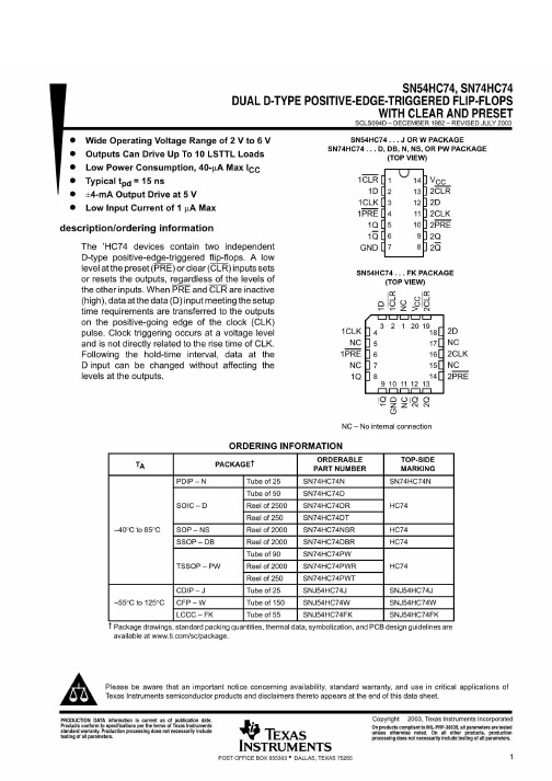
74HC74宽工作电压范围2 V 6 VD输出可以开车10 LSTTL LoadsD低功耗,40-µA马克斯ICCD典型信息= 15 nsD±4-mA输出驱动VD低输入电 流的5点1µA Maxdescription /订购informationThe HC74设备包含两个independentD-type positive-edge-triggered拖鞋。74HC74在预置(PRE)或 清除(CLR)输入设置或重置输出的低电平,而不考虑其他输入的电平。当PRE和CLR处于非活动状态(高)时,满足setuptime要求的数据 (D)输入处的数据被传输到时钟(CLK)脉冲正向边缘的输出端。时钟触发发生在电压水平,与CLK的上升时间没有直接关系。在保持时间 间隔之后,可以在不影响输出电平的情况下更改输入端的数据。订购包图纸,标准包装数量,74HC74热数据,符号,和PCB设计指南超 过“绝对最大额定值”下列出的应力可能对设备造成永久性损坏。这些只是应力等级,设备在这些或任何其他条件下的功能运行,超 出“推荐操作条件”的指示,是不受限制的。长时间暴露在绝对最大额定条件下可能会影响设备的可靠性。如果观察输入和输出电流额 定值,可能会超过输入和输出电压额定值。封装热阻抗按JESD 5计算环保(RoHS &没有某人/ Br): TI定义“绿色”意味着“Pb-Free”,此 外,使用包装材料,不含卤素,包括溴(Br)或锑(某人)总数的0.1%以上产品的重量。(3)实验室,峰值温度。湿度敏感性级别评级根据 JEDECindustry标准分类和soldertemperature峰值。重要信息和免责声明:本页所提供的信息代表德州仪器自提供之日起的知识和信念。TI 的知识和信念基于第三方提供的信息,对于这些信息的准确性不作任何陈述或保证。74HC74目前正在努力更好地整合来自第三方的信 息。TI已采取并将继续采取合理措施,提供具有代表性和准确的信息,但可能未对来料和化学品进行破坏性测试或化学分析。TI和TI供 应商认为某些信息是专有的,因此CAS号码和其他有限的信息可能无法发布。在任何情况下,TI因该等信息而产生的责任都不应超过 TIto客户在本文件中每年销售的TI部件的采购总价
IN74ACT21中文资料

D UAL 4-I NPUT AND G ATEHigh-Speed Silicon-Gate CMOSThe IN74ACT21 is identical in pinout to the LS/ALS21, HC/HCT21. The IN74ACT21 may be used as a level converter for interfacing TTL or NMOS outputs to High Speed CMOS inputs.• TTL/NMOS Compatible Input Levels• Outputs Directly Interface to CMOS, NMOS, and TTL • Operating Voltage Range: 4.5 to 5.5 V • Low Input Current: 1.0 µA; 0.1 µA @ 25°C •Outputs Source/Sink 24 mAORDERING INFORMATIONIN74ACT21N Plastic IN74ACT21D SOIC T A = -40° to 85° C for allpackagesPIN ASSIGNMENTNC = NO CONNECTIONFUNCTION TABLEInputs OutputA B C D Y L X X X L X L X X L X X L X L X X X L L H H H H H X = don’t careLOGIC DIAGRAMPIN 14 =V CC PIN 7 = GNDPINS 3,11 = NO CONNECTIONMAXIMUM RATINGS*Symbol Parameter ValueUnit V CC DC Supply Voltage (Referenced to GND) -0.5 to +7.0 VV IN DC Input Voltage (Referenced to GND) -0.5 to V CC +0.5 VV OUT DC Output Voltage (Referenced to GND) -0.5 to V CC +0.5 VI IN DC Input Current, per Pin ±20 mAI OUT DC Output Sink/Source Current, per Pin ±50 mAI CC DC Supply Current, V CC and GND Pins ±50 mAP D Power Dissipation in Still Air, Plastic DIP+ SOIC Package+ 750500mWTstg Storage Temperature -65 to +150 °CT L Lead Temperature, 1 mm from Case for 10Seconds(Plastic DIP or SOIC Package)260 °C*Maximum Ratings are those values beyond which damage to the device may occur.Functional operation should be restricted to the Recommended Operating Conditions.+Derating - Plastic DIP: - 10 mW/°C from 65° to 125°CSOIC Package: : - 7 mW/°C from 65° to 125°CRECOMMENDED OPERATING CONDITIONSSymbol Parameter MinMaxUnit V CC DC Supply Voltage (Referenced to GND) 4.5 5.5 VV IN, V OUT DC Input Voltage, Output Voltage (Referenced toGND)0 V CC VT J Junction Temperature (PDIP) 140 °CT A Operating Temperature, All Package Types -40 +85 °CI OH Output Current - High -24 mAI OL Output Current - Low 24 mAt r, t f Input Rise and Fall Time * (except Schmitt Inputs) V CC=4.5 VV CC =5.5 V108.0ns/V* VINfrom 0.8 V to 2.0 VThis device contains protection circuitry to guard against damage due to high static voltages or electric fields. However, precautions must be taken to avoid applications of any voltage higher than maximum rated voltages to this high-impedance circuit. For proper operation, V IN and V OUT should be constrained to the range GND≤(V IN or V OUT)≤V CC.Unused inputs must always be tied to an appropriate logic voltage level (e.g., either GND or V CC). Unused outputs must be left open.DC ELECTRICAL CHARACTERISTICS (Voltages Referenced to GND)V CC Guaranteed LimitsSymbol Parameter Test Conditions V 25 °C -40°C to85°CUnit V IH Minimum High-Level Input VoltageV OUT =0.1 V or V CC -0.1 V 4.5 5.5 2.0 2.0 2.0 2.0 VV IL Maximum Low -Level Input VoltageV OUT =0.1 V 4.5 5.5 0.8 0.8 0.8 0.8 VV OH Minimum High-Level Output VoltageI OUT ≤ -50 µA 4.5 5.5 4.4 5.4 4.4 5.4 V*V IN =V IHI OH =-24 mA I OH =-24 mA4.55.5 3.86 4.86 3.76 4.76 V OL Maximum Low-Level Output VoltageI OUT ≤ 50 µA 4.5 5.5 0.1 0.1 0.1 0.1 V*V IN =V IH or V ILI OL =24 mA I OL =24 mA 4.55.5 0.36 0.36 0.44 0.44 I IN Maximum Input Leakage CurrentV IN =V CC or GND 5.5 ±0.1 ±1.0 µA∆I CCT Additional MaxI CC /InputV IN =V CC - 2.1 V 5.5 1.5 mA I OLD +Minimum Dynamic Output CurrentV OLD =1.65 V Max 5.5 75 mAI OHD +Minimum Dynamic Output CurrentV OHD =3.85 V Min 5.5 -75 mAI CC Maximum Quiescent Supply Current(per Package)V IN =V CC or GND 5.5 4.0 40 µA*All outputs loaded; thresholds on input associated with output under test. +Maximum test duration 2.0 ms, one output loaded at a time.AC ELECTRICAL CHARACTERISTICS(V CC=5.0 V ± 10%, C L=50pF,Input t r=t f=3.0 ns)GuaranteedLimits Symbol Parameter 25 °C -40°C to85°CUnitMinMax MinMax t PLH Propagation Delay, Input A , B, C or D toOutput Y (Figure 1)1.5 8.5 1.0 9.0 nst PHL Propagation Delay, Input A , B, C or D toOutput Y (Figure 1)1.5 9.5 1.0 10.0nsC IN Maximum Input Capacitance 4.5 4.5 pFTypical @25°C,V CC=5.0VC PD Power Dissipation Capacitance 30 pFFigure 1. Switching Waveforms。
KK74VHC00中文资料
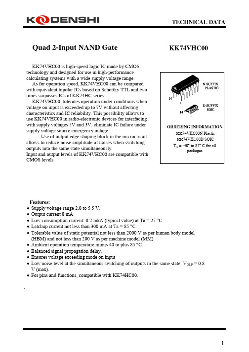
TECHNICAL DATAKK 74VHC00Quad 2-Input NAND GateKK 74VHC00 is high-speed logic IC made by CMOS technology and designed for use in high-performance calculating systems with a wide supply voltage range. As for operation speed, KK 74VHC00 can be compared with equivalent bipolar ICs based on Schottky TTL and two times surpasses ICs of KK 74НС series.KK 74VHC00 tolerates operation under conditions when voltage on input is exceeded up to 7V without affecting characteristics and IC reliability. This possibility allows to use KK 74VHC00 in radio-electronic devices for interfacing with supply voltages 5V and 3V, eliminate IC failure under supply voltage source emergency outage.Use of output edge shaping block in the microcircuit allows to reduce noise amplitude of noises when switching outputs into the same state simultaneously.Input and output levels of KK 74VHC00 are compatible with CMOS levelsFeatures:• Supply voltage range 2.0 to 5.5 V. • Output current 8 mA.• Low consumption current: 0.2 mkA (typical value) at Та = 25 °С. • Latchup current not less than 300 mA at Та = 85 °С.• Tolerable value of static potential not less than 2000 V as per human body model (HBM) and not less than 200 V as per machine model (ММ). • Ambient operation temperature minus 40 to plus 85°С. • Balanced signal propagation delay.• Ensures voltage exceeding mode on input• Low noise level at the simultaneous switching of outputs in the same state: V OLP = 0.8 V (max).• For pins and functions, compatible with KK 74НС00..KK74VHC00 truth tablePins description in KK74VHC00Absolute maximum conditions*Parameter, unit Symbol Valueminmax Supply voltage, V V CC-0.5 7.0Input voltage, V Vin -0.5 7.0Output voltage, V Vout -0.5 Vcc+0.5VInput diode current, mA Iik – -20Current of common output and supplyoutput, mAIcc – ± 75Output current, mA Iout – ± 25Output diode current, mA Iok – ± 20Dissipated power, mW Pd – 180*Under absolute maximum conditions operation of microcircuit is not guaranteed. Operation isguaranteed under maximum conditionsMaximum conditionsSymbol ValueParameter, unitminmax Supply voltage, V V CC 2.0 5.5Input voltage,V Vin 0 V CCOutput voltage, V Vout 0 V CCOutput current, mA Iout – ± 8.0Input rise and fall time, ns/V at Vcc = (3.3 ± 0.3) Vat Vcc = (5.0 ± 0.5) V t LH, t HL10020DC electrical characteristicsValue25 °C–40 to 85 °CSymbo l Parameter Test conditionsV CC ,V min max min maxUnit 2.01.5 – 1.5 – VV IHHigh input voltage–3.0-5.50.7Vcc– 0.7Vcc –2.0 – 0.5 – 0.5 V IL Low input voltage–3.0-5.5– 0.3Vcc – 0.3Vcc2.0 1.92– 1.9 –3.0 2.92– 2.9 –4.5 4.42– 4.4 – V I = V IH or V IL I O = -50 mkA5.5 5.52– 5.4 –V I = V IH or V IL ; I O = -4 mA3.0 2.58– 2.48 –V OHHigh output voltage V I = V IH or V IL ; I O = -8 mA4.5 3.94– 3.80 –2.0 – 0.09– 0.13.0 – 0.09– 0.14.5 – 0.09– 0.1 V I =V IH orV IL I O = 50 mkA 5.5 – 0.09– 0.1V I = V IH or V IL I O = 4 mA 3.0 – 0.36– 0.44V OLLow output voltage V I = V IH or V IL I O = 8 mA4.5 – 0.36– 0.44I OZ Output current in "off" stateV I = V IH or V IL V O = V CC or 0V 5.5 - ±0.25- ±2.5mkA I I Input current V I = 5.5V or 0V 0 – 5.5- ±0.1- ±1.0I CCConsumption current V I =V CC or 0V5.5 - 4.0 - 40.0AC electrical characteristics (t LH = t HL = 3.0 ns)Value25 °C–40to 85 °CSymbol Parameter Testconditi ons V CC , VC L , pF min max min maxUnit 15- 7.9- 9.5 3.3 ± 0.350 11.4 13.0 155.56.5 t PHL , t PLHPropagation delay time when switching "on", "off" Figure 2 5.0 ± 0.550 7.5 8.5ns C I Input capacity - 5.0 10 -C РDDynamic capacity V I = 0 V orV CC5.0 38 -pFNoise characteristics (C L = 50 pF)ValueSymbol Parameter V CC , V min maxUnit V OLP Positive noise of low output voltage 5.0 - 0.8 V V OLV Negative noise of low output voltage5.0 -0.8 - V IHD Input dynamic high voltage 5.0 3.5 - V ILDInput dynamic low voltage5.0-1.5- Time diagram of input and output pulsesVССGNDVCC0 V。
KK74LS04N中文资料

TECHNICAL DATAKK 74LS04Hex InvertersThis device contains six independent inverts. It performs the Boolean function Y=A.PIN ASSIGNMENTLOGIC DIAGRAMPIN 14 =V CCPIN 7 = GNDFUNCTION TABLEInputs Output A Y H L L HMAXIMUM RATINGS*Symbol Parameter ValueUnit V CC Supply Voltage 7.0 VV IN Input Voltage 7.0 VV OUT Output Voltage 7.0 VTstg Storage Temperature Range -65 to +150 °C*Maximum Ratings are those values beyond which damage to the device may occur.Functional operation should be restricted to the Recommended Operating Conditions.RECOMMENDED OPERATING CONDITIONSSymbol Parameter MinMaxUnit V CC Supply Voltage 4.75 5.25 VI OH High Level Output Current -400 VI OL Low Level Output Current 8.0 VT A Ambient Temperature Range 0 +70 °CDC ELECTRICAL CHARACTERISTICS over full operating conditionsGuaranteedLimit Symbol Parameter TestConditions MinMaxUnit V IH High Level Input Voltage 2 VV IL Low Level Input Voltage 0.8 VV IK Input Clamp Voltage V CC = min, I I = -18 mA -1.5 VV OH High Level Output Current V CC = min, V IL =maxI OH = max2.7 VV OL Low Level Output Voltage V CC = min, V IH =min,I OL = 8 mA 0.5VI I Input Current at maximum inputvoltageV CC = max, V I = -7V 0.1 mA I IH High Level Input Current V CC = max, V IN = 2.7 V 20 µA I IL Low Level Input Current V CC = max, V IN = 0.4 V -0.4 mA I OS Short-circuit output current V CC = max (Note) -20 -100 mAI CC Supply Current V CC = max Total withoutputs high 2.4mATotalwithoutputs low6.6 Note: Not more than one output should be shorted at a time, and duration should not exceed one second.AC ELECTRICAL CHARACTERISTICS (V CC = 5.0 V, C L = 15 pF, T A=25 °C, R L = 2 kΩ,t r =15 ns, t f = 6.0 ns)MaxUnit Symbol Parameter Mint PLH Propagation Delay Time 15 nst PHL Propagation Delay Time 15 nsFigure 1. Switching WaveformsNOTE A. C L includes probe and jig capacitance.Figure 2. Test Circuit。
- 1、下载文档前请自行甄别文档内容的完整性,平台不提供额外的编辑、内容补充、找答案等附加服务。
- 2、"仅部分预览"的文档,不可在线预览部分如存在完整性等问题,可反馈申请退款(可完整预览的文档不适用该条件!)。
- 3、如文档侵犯您的权益,请联系客服反馈,我们会尽快为您处理(人工客服工作时间:9:00-18:30)。
TECHNICAL DATA KK74ACT02 Quad 2-Input NOR Gate High-Speed Silicon-Gate CMOS
ORDERING INFORMATION KK74ACT02N Plastic KK74ACT02D SOIC TA = -40° to 85° C for all packages
The KK74ACT02 is identical in pinout to the LS/ALS02, HC/HCT02. The KK74ACT02 may be used as a level converter for interfacing TTL or NMOS outputs to High Speed CMOS inputs. • TTL/NMOS Compatible Input Levels • Outputs Directly Interface to CMOS, NMOS, and TTL • Operating Voltage Range: 4.5 to 5.5 V • Low Input Current: 1.0 µA; 0.1 µA @ 25°C • Outputs Source/Sink 24 mA
LOGIC DIAGRAM
PIN 14 =VCC PIN 7 = GND
PIN ASSIGNMENT FUNCTION TABLE Inputs Output A B Y L L H L H L H L L H H L
1
元器件交易网www.cecb2b.comKK74ACT02 MAXIMUM RATINGS*Symbol Parameter Value Unit VCCDC Supply Voltage (Referenced to GND) -0.5 to +7.0 V VINDC Input Voltage (Referenced to GND) -0.5 to VCC +0.5 V VOUTDC Output Voltage (Referenced to GND) -0.5 to VCC +0.5 V IINDC Input Current, per Pin ±20 mA IOUTDC Output Sink/Source Current, per Pin ±50 mA ICCDC Supply Current, VCC and GND Pins ±50 mA PDPower Dissipation in Still Air, Plastic DIP+ SOIC Package+ 750 500 mW
Tstg Storage Temperature -65 to +150 °C
TLLead Temperature, 1 mm from Case for 10 Seconds (Plastic DIP or SOIC Package) 260 °C
*Maximum Ratings are those values beyond which damage to the device may occur.
Functional operation should be restricted to the Recommended Operating Conditions. +Derating - Plastic DIP: - 10 mW/°C from 65° to 125°C SOIC Package: : - 7 mW/°C from 65° to 125°C
RECOMMENDED OPERATING CONDITIONS Symbol Parameter Min Max Unit VCCDC Supply Voltage (Referenced to GND) 4.5 5.5 V VIN, VOUTDC Input Voltage, Output Voltage (Referenced to GND) 0 VCCV TJJunction Temperature (PDIP) 140 °C
TAOperating Temperature, All Package Types -40 +85 °C
IOHOutput Current - High -24 mA IOLOutput Current - Low 24 mA tr, tfInput Rise and Fall Time * (except Schmitt Inputs) VCC =4.5 V VCC =5.5 V 0 0 10 8.0 ns/V
* VIN from 0.8 V to 2.0 V
This device contains protection circuitry to guard against damage due to high static voltages or electric fields. However, precautions must be taken to avoid applications of any voltage higher than maximum rated voltages to this high-impedance circuit. For proper operation, VIN and VOUT should be constrained to the range GND≤(VIN or VOUT)≤VCC. Unused inputs must always be tied to an appropriate logic voltage level (e.g., either GND or VCC). Unused
outputs must be left open.
2
元器件交易网www.cecb2b.comKK74ACT02 DC ELECTRICAL CHARACTERISTICS (Voltages Referenced to GND)
VCCGuaranteed Limits
Symbol Parameter Test Conditions V 25 °C -40°C to
85°C Unit
VIHMinimum High-Level Input Voltage VOUT=0.1 V 4.55.52.0 2.0 2.0 2.0 V VILMaximum Low -Level Input Voltage VOUT=0.1 V or VCC-0.1 V 4.55.50.8 0.8 0.8 0.8 V VOHMinimum High-Level Output Voltage IOUT ≤ -50 µA 4.55.54.4 5.4 4.4 5.4 V *VIN= VIL
IOH=-24 mA IOH=-24 mA 4.55.5 3.86
4.86 3.76
4.76
VOLMaximum Low-Level Output Voltage IOUT ≤ 50 µA 4.55.50.1 0.1 0.1 0.1 V
*VIN=VIH or VIL
IOL=24 mA IOL=24 mA 4.55.5 0.36
0.36 0.44
0.44
IINMaximum Input Leakage Current VIN=VCC or GND 5.5±0.1 ±1.0 µA
∆ICCTAdditional Max ICC/Input VIN=VCC - 2.1 V 5.5 1.5 mA
IOLD+Minimum Dynamic Output Current VOLD=1.65 V Max 5.5 75 mA IOHD+Minimum Dynamic Output Current VOHD=3.85 V Min 5.5 -75 mA ICCMaximum Quiescent Supply Current (per Package) VIN=VCC or GND 5.54.0 40 µA
* All outputs loaded; thresholds on input associated with output under test.
+Maximum test duration 2.0 ms, one output loaded at a time.
3
元器件交易网www.cecb2b.comKK74ACT02 AC ELECTRICAL CHARACTERISTICS (VCC=5.0 V ± 10%, CL=50pF,Input tr=tf=3.0 ns)
Guaranteed Limits Symbol Parameter 25 °C -40°C to 85°C Unit MinMaxMin Max tPLHPropagation Delay, Input A or B to Output Y (Figure 1) 1.5 8.5 1.0 9.0 ns
tPHLPropagation Delay, Input A or B to Output Y (Figure 1) 1.5 9.5 1.0 10 ns CINMaximum Input Capacitance 4.5 4.5 pF Typical @25°C,VCC=5.0 V
CPDPower Dissipation Capacitance 30 pF
Figure 1. Switching Waveforms 4
元器件交易网www.cecb2b.com