STM802S中文资料
平头哥半导体有限公司S802用户手册说明书
NumberRevision 1.2.15 Security Public Date 2017-07-28Copyright © 2019 T-HEAD Semiconductor Co.,Ltd. All rights reserved.This document is the property of T-HEAD Semiconductor Co.,Ltd. This document may only be distributed to: (i) a T-HEAD party having a legitimate business need for the information contained herein, or (ii) a non-T-HEAD party having a legitimate business need for the information contained herein. No license, expressed or implied, under any patent, copyright or trade secret right is granted or implied by the conveyance of this document. No part of this document may be reproduced, transmitted, transcribed, stored in a retrieval system, translated into any language or computer language, in any form or by any means, electronic, mechanical, magnetic, optical, chemical, manual, or otherwise without the prior written permission of T-HEAD Semiconductor Co.,Ltd.Trademarks and PermissionsThe T-HEAD Logo and all other trademarks indicated as such herein are trademarks of T-HEAD Semiconductor Co.,Ltd. All other products or service names are the property of their respective owners. NoticeThe purchased products, services and features are stipulated by the contract made between T-HEAD and the customer. All or part of the products, services and features described in this document may not be within the purchase scope or the usage scope. Unless otherwise specified in the contract, all statements, information, and recommendations in this document are provided "AS IS" without warranties, guarantees or representations of any kind, either express or implied.The information in this document is subject to change without notice. Every effort has been made in the preparation of this document to ensure accuracy of the contents, but all statements, information, and recommendations in this document do not constitute a warranty of any kind, express or implied.Copyright © 2019 平头哥半导体有限公司,保留所有权利.本文档的产权属于平头哥半导体有限公司(下称平头哥)。
西门子802S操作说明
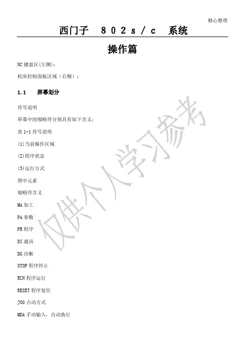
精心整理西门子 802s/c 系统操作篇NC 键盘区(左侧):机床控制面板区域(右侧):1.1 屏幕划分表1-1(1)(2)(3)MA 加工PA 参数PR 程序DI 通讯DG 诊断STOP 程序停止RUN 程序运行RESET 程序复位JOG 点动方式MDA 手动输入,自动执行AUTO自动方式表1-1符号说明(续)图中元素缩略符含义SKP程序段跳跃跳步的程序段在其段号之前用一斜线示,这些程DRYROV(4)SBL停。
SBLM1程序停止此功能生效时程序运行到有M01指令的程序段时停止运行。
此时屏幕上显示“停止M00/M01 有效”。
PRT程序测试(无指令给驱动)1_1000INC步进增量系统处于JOG运行方式时不显示程序控制而是显示所选择的步进增量。
开机和回参考点2式。
3在CNC输入/3.1功能刀具参数包括刀具几何参数、磨损量参数和刀具型号参数。
不同类型的刀具均有一个确定的参数数量。
每个刀具有一个刀具号(T号)。
参见章节8.6“刀具和刀具补偿”。
参数设定软键选择接下去渐低的或渐高的刀沿号选择接下去渐低的或渐高的刀具号计算刀具长度补偿值。
在内按“确认键”3.1.刀具补偿分为刀具长度补偿和刀具半径补偿。
参数表结构因刀具类型不同而不同3.1。
3对刀确定刀具补偿值功能利用此功能可以计算刀具T未知的几何长度前提条件换入该刀具。
在JOG方式下移动该刀具,使刀尖到达一个已知坐标值的机床位置,这可能是一个已知位置的工件。
其坐标值可以分为两个部分:可存储的零点偏置和偏移值(Offset)过程偏移值登记到“偏移值”区域。
选择相应的零点偏置(比如:G54),没有零点偏置时选择G500。
每次必须对所选择的坐标轴分别进行登记(参见图3-6)。
注意:利用F计算出所在坐标轴的刀补长度1或2,按“确认键”,计算出的补偿值将被存储。
3.2输入/修改零点偏置值—“参数”操作区功能在回参考点之后实际值存储器以及实际值的显示均以机床零点为基准,而工件的加工程序则以工件零点为基准,这之间的差值就作为可设定的零点偏移量输入操作步骤操作步骤只有使用已知的刀具才可以计算零点偏置。
西门子802S数控车床基本组成
西门子802S数控车床基本组成西门子802S数控系统电气主要组成部分有,CNC系统(包括ECU)、主轴驱动控制系统、进给驱动控制系统(包括伺服驱动控制系统、步进驱动控制系统)、辅助装置(包括刀架控制系统、润滑、冷却控制系统)及PLC输入输出转接口,机械结构部分主要有,机床床身、导轨、工作台、刀架等。
(其中刀架在第3章有具体介绍)2.1 CNC系统计算机数控系统(Computer Numerical Control)简称CNC系统,是一种用计算机通过执行其存储器内的程序来实现数控功能,并配有接口电路和伺服驱动装置的专用计算机系统。
数控机床在CNC系统的控制下,自动地按给定的加工程序加工出工件。
所以计算机数控系统是一种计算机在内的数字控制系统。
CNC系统是一种位置控制系统。
其控制过程是根据输入的信息(加工程序),进行数据处理、插补运算、获得理想的运动轨迹信息,然后输出到执行部件,加工出所需要的工件。
CNC系统的核心是CNC装置。
由于采用了计算机,使CNC装置的性能提高,促使CNC系统迅速发展。
CNC 装置的工作流程主要分为输入、译码、刀具补偿、进给速度处理、插补和位置控制。
输入的任务是把加工程序、控制参数和补偿数据输入到CNC 装置中去,输入的方法有纸带阅读机输入、键盘输入、磁带和磁盘输入以及通信方式输入。
CNC 的工作方式一般有两种,一种是边输入边加工,即在前一个程序段在加工时,输入后一个程序段的内容;另一种是一次性的将整个工件加工程序输入到CNC 装置的内部存储器中,加工时再把程序段从存储器中一个一个的调出来进行处理。
随着大规模集成电路技术和表面安装技术的发展,CNC 系统硬件块及安装方式不断改进。
从CNC 系统的总体安装结构看,有整体式结构和分体式结构两种。
从CNC 系统使用的CPU及结构来分,CNC 系统的硬件结构一般分为单CPU 和多CPU 结构两大类。
初期的CNC 系统和现在的一些经济型CNC 系统采用单CPU 结构,而多CPU 结构可以满足数控机床高进速度、高加工精度和许多复杂功能的要求,也适应于并入FMS 和CIMS 运行的需要,从而得到了迅速的发展,它反映了当今数控系统的新水平。
802S参数说明

4、31020 电机编码器线数
5、32000 轴的最大速度
6、32010 快速点速度
7、32020 手动点动速度
8、36200 最大速度监控,一般
注:详细说明见802S简明安装调试手册4-18
802S参数说明
一、 系统参数说明及更改:各进给轴
1 32000 轴的最大速度
2 32010 快速点速度
3 32020 手动点动速度
4 31030 丝杠螺距
5 31020 电机编码器线数
6 14510[14] 润滑时间间隔 单位1min
7 14510[15] 润滑时间 单位0.1S
8 32450 反向间隙
9 36100 负软限位
10 36110 正软限位
11 30130 脉冲输出,设置参数为2
12 30240 编码器内部反馈, 设置参数为3 注:详细源自明见802S简明安装调试手册4-1
二、系统参数说明及更改:主轴参数
1、30130 主轴有无模拟量输出 设置为1表示有模拟量输出
2、30134 单极性主轴和双极性主轴设置 设置为0表示双极性主轴,1表示单极性主轴
STM802SM6F中文资料
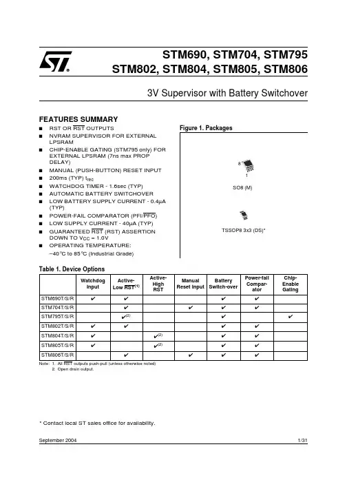
1/31September 2004STM690, STM704, STM795STM802, STM804, STM805, STM8063V Supervisor with Battery Switchover* Contact local ST sales office for availability.FEATURES SUMMARY■■NVRAM SUPERVISOR FOR EXTERNAL LPSRAM■CHIP-ENABLE GATING (STM795 only) FOR EXTERNAL LPSRAM (7ns max PROP DELAY)■MANUAL (PUSH-BUTTON) RESET INPUT ■200ms (TYP) t rec■WATCHDOG TIMER - 1.6sec (TYP)■AUTOMATIC BATTERY SWITCHOVER■LOW BATTERY SUPPLY CURRENT - 0.4µA (TYP)■POWER-FAIL COMPARATOR (PFI/PFO)■LOW SUPPLY CURRENT - 40µA (TYP)■GUARANTEED RST (RST) ASSERTION DOWN TO V CC = 1.0V■OPERATING TEMPERATURE:–40°C to 85°C (Industrial Grade)Table 1. Device OptionsNote: 1.2.Open drain output.Watchdog InputActive- Low RST (1)Active- High RSTManual Reset Input Battery Switch-overPower-fail Compar-atorChip-Enable GatingSTM690T/S/R ✔✔✔✔STM704T/S/R ✔✔✔✔STM795T/S/R ✔(2)✔✔STM802T/S/R ✔✔✔✔STM804T/S/R ✔✔(2)✔✔STM805T/S/R ✔✔(2)✔✔STM806T/S/R✔✔✔✔STM690/704/795/802/804/805/806TABLE OF CONTENTSFEATURES SUMMARY . . . . . . . . . . . . . . . . . . . . . . . . . . . . . . . . . . . . . . . . . . . . . . . . . . . . . . . . . . . . .1Figure 1.Packages. . . . . . . . . . . . . . . . . . . . . . . . . . . . . . . . . . . . . . . . . . . . . . . . . . . . . . . . . . . . . .1 Table 1.Device Options . . . . . . . . . . . . . . . . . . . . . . . . . . . . . . . . . . . . . . . . . . . . . . . . . . . . . . . . .1SUMMARY DESCRIPTION. . . . . . . . . . . . . . . . . . . . . . . . . . . . . . . . . . . . . . . . . . . . . . . . . . . . . . . . . . .4Figure 2.Logic Diagram (STM690/802/804/805) . . . . . . . . . . . . . . . . . . . . . . . . . . . . . . . . . . . . . . .4 Figure 3.Logic Diagram (STM704/806) . . . . . . . . . . . . . . . . . . . . . . . . . . . . . . . . . . . . . . . . . . . . . .4 Figure 4.Logic Diagram (STM795). . . . . . . . . . . . . . . . . . . . . . . . . . . . . . . . . . . . . . . . . . . . . . . . . .4 Table 2.Signal Names . . . . . . . . . . . . . . . . . . . . . . . . . . . . . . . . . . . . . . . . . . . . . . . . . . . . . . . . . .4 Figure 5.STM690/802/804/805 Connections. . . . . . . . . . . . . . . . . . . . . . . . . . . . . . . . . . . . . . . . . .5 Figure 6.STM704/806 Connections. . . . . . . . . . . . . . . . . . . . . . . . . . . . . . . . . . . . . . . . . . . . . . . . .5 Figure 7.STM795 Connections . . . . . . . . . . . . . . . . . . . . . . . . . . . . . . . . . . . . . . . . . . . . . . . . . . . .5 Pin Descriptions . . . . . . . . . . . . . . . . . . . . . . . . . . . . . . . . . . . . . . . . . . . . . . . . . . . . . . . . . . . . . . .6 Table 3.Pin Description. . . . . . . . . . . . . . . . . . . . . . . . . . . . . . . . . . . . . . . . . . . . . . . . . . . . . . . . . .6 Figure 8.Block Diagram (STM690/802/804/805). . . . . . . . . . . . . . . . . . . . . . . . . . . . . . . . . . . . . . .7 Figure 9.Block Diagram (STM704/806). . . . . . . . . . . . . . . . . . . . . . . . . . . . . . . . . . . . . . . . . . . . . .7 Figure 10.Block Diagram (STM795) . . . . . . . . . . . . . . . . . . . . . . . . . . . . . . . . . . . . . . . . . . . . . . . . .8 Figure 11.Hardware Hookup. . . . . . . . . . . . . . . . . . . . . . . . . . . . . . . . . . . . . . . . . . . . . . . . . . . . . . .8OPERATION . . . . . . . . . . . . . . . . . . . . . . . . . . . . . . . . . . . . . . . . . . . . . . . . . . . . . . . . . . . . . . . . . . . . . .9Reset Output . . . . . . . . . . . . . . . . . . . . . . . . . . . . . . . . . . . . . . . . . . . . . . . . . . . . . . . . . . . . . . . . . .9 Push-button Reset Input (STM704/806). . . . . . . . . . . . . . . . . . . . . . . . . . . . . . . . . . . . . . . . . . . . .9 Watchdog Input (NOT available on STM704/795/806) . . . . . . . . . . . . . . . . . . . . . . . . . . . . . . . . .9 Back-up Battery Switchover. . . . . . . . . . . . . . . . . . . . . . . . . . . . . . . . . . . . . . . . . . . . . . . . . . . . . .9 Table 4.I/O Status in Battery Back-up . . . . . . . . . . . . . . . . . . . . . . . . . . . . . . . . . . . . . . . . . . . . ..9 Chip-Enable Gating (STM795 only) . . . . . . . . . . . . . . . . . . . . . . . . . . . . . . . . . . . . . . . . . . . . . . .10 Chip Enable Input (STM795 only). . . . . . . . . . . . . . . . . . . . . . . . . . . . . . . . . . . . . . . . . . . . . . . . .10 Chip Enable Output (STM795 only) . . . . . . . . . . . . . . . . . . . . . . . . . . . . . . . . . . . . . . . . . . . . . . .10 Figure 12.Chip-Enable Gating. . . . . . . . . . . . . . . . . . . . . . . . . . . . . . . . . . . . . . . . . . . . . . . . . . . . .10 Figure 13.Chip Enable Waveform (STM795) . . . . . . . . . . . . . . . . . . . . . . . . . . . . . . . . . . . . . . . . .10 Power-fail Input/Output (NOT available on STM795) . . . . . . . . . . . . . . . . . . . . . . . . . . . . . . . . .11 Applications Information . . . . . . . . . . . . . . . . . . . . . . . . . . . . . . . . . . . . . . . . . . . . . . . . . . . . . . .11 Figure 14.Power-fail Comparator Waveform (STM690/704/802/804/805/806). . . . . . . . . . . . . . . .11 Using a SuperCap™ as a Backup Power Source. . . . . . . . . . . . . . . . . . . . . . . . . . . . . . . . . . . .12 Figure ing a SuperCap™. . . . . . . . . . . . . . . . . . . . . . . . . . . . . . . . . . . . . . . . . . . . . . . . . . . .12 Negative-Going V CC Transients. . . . . . . . . . . . . . . . . . . . . . . . . . . . . . . . . . . . . . . . . . . . . . . . . .12TYPICAL OPERATING CHARACTERISTICS . . . . . . . . . . . . . . . . . . . . . . . . . . . . . . . . . . . . . . . . . . .13Figure 16.V BAT-to-V OUT On-Resistance vs. Temperature. . . . . . . . . . . . . . . . . . . . . . . . . . . . . . . .13 Figure 17.Supply Current vs. Temperature (no load) . . . . . . . . . . . . . . . . . . . . . . . . . . . . . . . . . . .13 Figure 18.V PFI Threshold vs. Temperature. . . . . . . . . . . . . . . . . . . . . . . . . . . . . . . . . . . . . . . . . . .14 Figure 19.Reset Comparator Propagation Delay vs. Temperature. . . . . . . . . . . . . . . . . . . . . . . . .14 Figure 20.Power-up t rec vs. Temperature . . . . . . . . . . . . . . . . . . . . . . . . . . . . . . . . . . . . . . . . . . . .142/31STM690/704/795/802/804/805/806Figure 21.Normalized Reset Threshold vs. Temperature . . . . . . . . . . . . . . . . . . . . . . . . . . . . . . . .15 Figure 22.Watchdog Time-out Period vs. Temperature . . . . . . . . . . . . . . . . . . . . . . . . . . . . . . . . .15 CON On-Resistance vs. Temperature . . . . . . . . . . . . . . . . . . . . . . . . . . . . . . . . . .15 Figure 24.PFI to PFO Propagation Delay vs. Temperature. . . . . . . . . . . . . . . . . . . . . . . . . . . . . . .16 Figure 25.RST Output Voltage vs. Supply Voltage. . . . . . . . . . . . . . . . . . . . . . . . . . . . . . . . . . . . .16 Figure 26.RST Output Voltage vs. Supply Voltage. . . . . . . . . . . . . . . . . . . . . . . . . . . . . . . . . . . . .17 Figure 27.RST Response Time (Assertion). . . . . . . . . . . . . . . . . . . . . . . . . . . . . . . . . . . . . . . . . . .17 Figure 28.RESET Response Time (Assertion) . . . . . . . . . . . . . . . . . . . . . . . . . . . . . . . . . . . . . . . .18 Figure 29.Power-fail Comparator Response Time (Assertion) . . . . . . . . . . . . . . . . . . . . . . . . . . . .18 Figure 30.Power-fail Comparator Response Time (De-Assertion) . . . . . . . . . . . . . . . . . . . . . . . . .19 Figure 31.V CC to Reset Propagation Delay vs. Temperature . . . . . . . . . . . . . . . . . . . . . . . . . . . . .19 Figure 32.Maximum Transient Duration vs. Reset Threshold Overdrive. . . . . . . . . . . . . . . . . . . . .20CON Propagation Delay vs. Temperature . . . . . . . . . . . . . . . . . . . . . . . . . . . . . . .20 MAXIMUM RATING. . . . . . . . . . . . . . . . . . . . . . . . . . . . . . . . . . . . . . . . . . . . . . . . . . . . . . . . . . . . . . . .21 Table 5.Absolute Maximum Ratings. . . . . . . . . . . . . . . . . . . . . . . . . . . . . . . . . . . . . . . . . . . . . . .21 DC and AC PARAMETERS . . . . . . . . . . . . . . . . . . . . . . . . . . . . . . . . . . . . . . . . . . . . . . . . . . . . . . . . .21Table 6.Operating and AC Measurement Conditions. . . . . . . . . . . . . . . . . . . . . . . . . . . . . . . . . .21 Figure 34.E to ECON Propagation Delay Test Circuit. . . . . . . . . . . . . . . . . . . . . . . . . . . . . . . . . . .22 Figure 35.AC Testing Input/Output Waveforms. . . . . . . . . . . . . . . . . . . . . . . . . . . . . . . . . . . . . . . .22 Figure 36.MR Timing Waveform . . . . . . . . . . . . . . . . . . . . . . . . . . . . . . . . . . . . . . . . . . . . . . . . . . .22 Figure 37.Watchdog Timing . . . . . . . . . . . . . . . . . . . . . . . . . . . . . . . . . . . . . . . . . . . . . . . . . . . . . .23 Table 7.DC and AC Characteristics . . . . . . . . . . . . . . . . . . . . . . . . . . . . . . . . . . . . . . . . . . . . . . .23PACKAGE MECHANICAL . . . . . . . . . . . . . . . . . . . . . . . . . . . . . . . . . . . . . . . . . . . . . . . . . . . . . . . . . .26 Figure 38.SO8 – 8-lead Plastic Small Outline, 150 mils body width, Package Mech. Drawing. . . .26 Table 8.SO8 – 8-lead Plastic Small Outline, 150 mils body width, Package Mechanical Data . .26 Figure 39.TSSOP8 – 8-lead, Thin Shrink Small Outline, 3x3mm body size, Outline . . . . . . . . . . .27 Table 9.TSSOP8 – 8-lead, Thin Shrink Small Outline, 3x3mm body size, Mechanical Data. . . .27PART NUMBERING . . . . . . . . . . . . . . . . . . . . . . . . . . . . . . . . . . . . . . . . . . . . . . . . . . . . . . . . . . . . . . .28 Table 10.Ordering Information Scheme . . . . . . . . . . . . . . . . . . . . . . . . . . . . . . . . . . . . . . . . . . . . .28 Table 11.Marking Description. . . . . . . . . . . . . . . . . . . . . . . . . . . . . . . . . . . . . . . . . . . . . . . . . . . . .29REVISION HISTORY. . . . . . . . . . . . . . . . . . . . . . . . . . . . . . . . . . . . . . . . . . . . . . . . . . . . . . . . . . . . . . .30 Table 12.Document Revision History. . . . . . . . . . . . . . . . . . . . . . . . . . . . . . . . . . . . . . . . . . . . . . .303/31STM690/704/795/802/804/805/8064/31SUMMARY DESCRIPTIONThe STM690/704/795/802/804/805/806 Supervi-sors are self-contained devices which provide mi-croprocessor supervisory functions with the ability to non-volatize and write-protect external LPSRAM. A precision voltage reference and com-parator monitors the V CC input for an out-of-toler-ance condition. When an invalid V CC condition high in the case of RST). These devices also offer a watchdog timer (except for STM704/795/806) as well as a power-fail comparator (except for STM795) to provide the system with an early warning of impending power failure.These devices are available in a standard 8-pin SOIC package or a space-saving 8-pin TSSOP package.Note: 1.For STM804/805, reset output is active-high and opendrain.Table 2. Signal NamesNote: 1.Open drain for STM804/805 only.2.STM795MR Push-button Reset Input WDIWatchdog InputRST Active-Low Reset Output RST (1)Active-High Reset Output E (2)Chip Enable InputE CON (2)Conditioned Chip Enable Output Vccsw (2)V CC Switch Output V OUTSupply Voltage Output V CC Supply Voltage V BAT Back-up Supply Voltage PFI Power-fail Input PFO Power-fail Output V SSGroundSTM690/704/795/802/804/805/806drain.5/31STM690/704/795/802/804/805/8066/31Pin DescriptionsA logic low on /MR asserts the reset output.Reset remains asserted as long as MR is low and for t rec after MR returns high. This active-low inputhas an internal pull-up. It can be driven from a TTL or CMOS logic line, or shorted to ground with a switch. Leave open if unused.WDI.If WDI remains high or low for 1.6sec, the in-ternal watchdog timer runs out and reset is trig-gered. The internal watchdog timer clears while reset is asserted or when WDI sees a rising or fall-ing edge.The watchdog function cannot be disabled by al-lowing the WDI pin to float.Pulses low for t rec when triggered, and stayslow whenever V CC is below the reset threshold or when MR is a logic low. It remains low for t rec after either V CC rises above the reset threshold, the watchdog triggers a reset, or MR goes from low tohigh.RST (Open Drain).Pulses high for t rec when trig-gered, and stays high whenever V CC is above the reset threshold or when MR is a logic high. It re-mains high for t rec after either V CC falls below thereset threshold, the watchdog triggers a reset, orMR goes from high to low.PFI.When PFI is less than V PFI or when V CC falls below V SW remains high. Connect to ground if unused.When PFI is less than V PFI , or V CC falls be-low V SW high. Leave open if unused.V OUT .When V CC is above the switchover voltage(V SO ), V OUT is connected to V CC through a P-channel MOSFET switch. When V CC falls belowV SO , V BAT connects to V OUT . Connect to V CC if no battery is used.When V OUT switches to battery, Vccsw ishigh. When V OUT switches back to V CC low. It can be used to drive gate of external PMOS transistor for I OUT requirements exceeding 75mA.The input to the chip-enable gating circuit. Con-nect to ground if unused.CON .CON goes low only when E is low and re-set is not asserted. If E CON is low when reset is as-CON goes high, whichever occurs first. In the disabled CON is pulled up to V OUT .V BAT .When V CC falls below V SO , V OUT switchesfrom V CC to V BAT . When V CC rises above V SO +hysteresis, V OUT reconnects to V CC . V BAT may ex-ceed V CC . Connect to V CC if no battery is used.Table 3. Pin DescriptionPinNameFunctionSTM795STM690STM802STM704STM806STM804STM805––6–MR Push-button Reset Input –6–6WDI Watchdog Input777–RST Active-Low Reset Output –––7RST Active-High Reset Output –444PFI PFI Power-fail Input –555PFO PFO Power-fail Output1111V OUT Supply Output for External LPSRAM 2222V CC Supply Voltage 3–––Vccsw V CC Switch Output 4333V SS Ground5–––E Chip Enable Input6–––E CON Conditioned Chip Enable Output 8888V BATBackup-Battery InputSTM690/704/795/802/804/805/806Note: 1.For STM804/805, reset output is active-high and open drain.7/31STM690/704/795/802/804/805/806Note: 1.For STM690/802/804/805.2.For STM795 only.3.Not available on STM795.4.For STM704/806.8/31STM690/704/795/802/804/805/806 OPERATIONReset OutputThe STM690/704/795/802/804/805/806 Supervi-sor asserts a reset signal to the MCU whenever V CC goes below the reset threshold (V RST), a watchdog time-out occurs, or when the Push-but-ton Reset Input (MR) is taken low. RST is guaran-teed to be a logic low (logic high for STM804/805) for 0V < V CC < V RST if V BAT is greater than 1V. Without a back-up battery, RST is guaranteed val-id down to V CC =1V.During power-up, once V CC exceeds the reset threshold an internal timer keeps RST low for the reset time-out period, t rec. After this interval RST returns high.If V CC drops below the reset threshold, RST goes low. Each time RST is asserted, it stays low for at least the reset time-out period (t rec). Any time V CC goes below the reset threshold the internal timer clears. The reset timer starts when V CC returns above the reset threshold.Push-button Reset Input (STM704/806)A logic low on MR asserts reset. Reset remains asserted while MR is low, and for t rec (see Figure 36.,page22) after it returns high. The MR input has an internal 40kΩ pull-up resistor, allowing it to be left open if not used. This input can be driven with TTL/CMOS-logic levels or with open-drain/ collector outputs. Connect a normally open mo-ual reset function; external debounce circuitry is the device is used in a noisy environment, connect a 0.1µF capacitor from MR to GND to provide ad-V CC when not used.Watchdog Input (NOT available on STM704/ 795/806)The watchdog timer can be used to detect an out-of-control MCU. If the MCU does not toggle the Watchdog Input (WDI) within t WD (1.6sec typ), the reset is asserted. The internal watchdog timer is cleared by either:1. a reset pulse, or2.by toggling WDI (high-to-low or low-to-high),which can detect pulses as short as 50ns. If WDI is tied high or low, a reset pulse istriggered every 1.8sec (t WD + t rec).The timer remains cleared and does not count for as long as reset is asserted. As soon as reset is re-leased, the timer starts counting (see Figure 37.,page23).Note: Input frequency greater than 20ns (50MHz) will be filtered.Back-up Battery SwitchoverIn the event of a power failure, it may be necessary to preserve the contents of external SRAM through V OUT. With a backup battery installed with voltage V BAT, the devices automatically switch the SRAM to the back-up supply when V CC falls. Note: If back-up battery is not used, connect both V BAT and V OUT to V CC.This family of Supervisors does not always con-nect V BAT to V OUT when V BAT is greater than V CC. V BAT connects to V OUT (through a 100Ω switch) when V CC is below V SW (2.4V) or V BAT (whichever is lower). This is done to allow the back-up battery (e.g., a 3.6V lithium cell) to have a higher voltage than V CC.Assuming that V BAT > 2.0V, switchover at V SO en-sures that battery back-up mode is entered before V OUT gets too close to the 2.0V minimum required to reliably retain data in most external SRAMs. When V CC recovers, hysteresis is used to avoid oscillation around the V SO point. V OUT is connect-ed to V CC through a 3Ω PMOS power switch. Note: The back-up battery may be removed while V CC is valid, assuming V BAT is adequately decou-pled (0.1µF typ), without danger of triggering a re-set.Table 4. I/O Status in Battery Back-up Pin StatusV OUT Connected to V BAT through internal switchV CC Disconnected from V OUTPFI DisabledPFO Logic LowE High impedanceE CON Logic HighWDI Watchdog timer is disabledMR DisabledRST Logic LowRST Logic HighV BAT Connected to V OUTVccsw Logic High (STM795)9/31STM690/704/795/802/804/805/80610/31Chip-Enable Gating (STM795 only)vents erroneous data from corrupting the external CMOS RAM in the event of an undervoltage con-dition. The STM795 uses a series transmission gate from E to E CON (see Figure 12). During nor-mal operation (reset not asserted), the E transmis-sion gate is enabled and passes all E transitions.When reset is asserted, this path becomes dis-abled, preventing erroneous data from corrupting the CMOS RAM. The short E propagation delay from E to E CON enables the STM795 to be used with most µPs. If E is low when reset asserts,CON remains low for typically 10µs to permit the current WRITE cycle to complete.Chip Enable Input (STM795 only)The chip-enable transmission gate is disabled and E is high impedance (disabled mode) while reset is asserted. During a power-down sequence when V CC passes the reset threshold, the chip-enable transmission gate disables and E immediately be-comes high impedance if the voltage at E is high.transmission gate will disable 10µs after reset as-serts (see Figure 13). This permits the current WRITE cycle to complete during power-down.Any time a reset is generated, the chip-enable transmission gate remains disabled and E remains high impedance (regardless of E activity) for the first half of the reset time-out period (t rec /2). When the chip enable transmission gate is enabled, the impedance of E appears as a 40Ω resistor in se-ries with the load at E CON . The propagation delay through the chip-enable transmission gate de-pends on V CC , the source impedance of the drive connected to E, and the loading on E CON . The chip enable propagation delay is production tested from the 50% point on E to the 50% point on E CON using a 50Ω driver and a 50pF load capacitance (see Figure 35.,page 22). For minimum propaga-CON and use a low-output impedance driver.Chip Enable Output (STM795 only)When the chip-enable transmission gate is en-CON is equivalent to a 40Ω resistor in series with the source driving E. In the disabled mode, the transmission gate is off CON to V OUT (see Figure 12). This pull-up turns off when the trans-mission gate is enabled.Power-fail Input/Output (NOT available on STM795)The Power-fail Input (PFI) is compared to an inter-nal reference voltage (independent from the V RST comparator). If PFI is less than the power-fail threshold (V PFI), the Power-Fail Output (PFO) will go low. This function is intended for use as an un-dervoltage detector to signal a failing power sup-ply. Typically PFI is connected through an external voltage divider (see Figure 11.,page8) to either the unregulated DC input (if it is available) or the regulated output of the V CC regulator. The voltage divider can be set up such that the voltage at PFI falls below V PFI several milliseconds before the regulated V CC input to the STM690/704/795/802/ 804/805/806 or the microprocessor drops below the minimum operating voltage.During battery back-up, the power-fail comparator Figure 14.,page11). This occurs after V CC drops below V SW (2.4V). When power returns, the pow-er-fail comparator is enabled and PFO follows PFI. If the comparator is unused, PFI should be con-nected to V SS and PFO left unconnected. PFO may be connected to MR on the STM704/806 so that a low voltage on PFI will generate a reset out-put.Applications InformationThese Supervisor circuits are not short-circuit pro-tected. Shorting V OUT to ground - excluding pow-er-up transients such as charging a decoupling capacitor - destroys the device. Decouple both V CC and V BAT pins to ground by placing 0.1µF ca-pacitors as close to the device as possible.11/31Using a SuperCap™ as a Backup Power SourceSuperCaps™ are capacitors with extremely high capacitance values (e.g., order of 0.47F) for their size. Figure 15 shows how to use a SuperCap as a back-up power source. The SuperCap may be connected through a diode to the V CC supply. Since V BAT can exceed V CC while V CC is above the reset threshold, there are no special precau-tions when using these supervisors with a Super-Cap.Negative-Going V CC TransientsThe STM690/704/795/802/804/805/806 Supervi-sors are relatively immune to negative-going V CC transients (glitches). Figure 32.,page20 was gen-erated using a negative pulse applied to V CC, starting at V RST + 0.3V and ending below the reset threshold by the magnitude indicated (comparator overdrive). The graph indicates the maximum pulse width a negative V CC transient can have without causing a reset pulse. As the magnitude of the transient increases (further below the thresh-old), the maximum allowable pulse width decreas-es. Any combination of duration and overdrive which lies under the curve will NOT generate a re-set signal. Typically, a V CC transient that goes 100mV below the reset threshold and lasts 40µs or less will not cause a reset pulse. A 0.1µF bypass capacitor mounted as close as possible to the V CC pin provides additional transient immunity.12/31TYPICAL OPERATING CHARACTERISTICSNote: Typical values are at T A = 25°C.13/3114/3115/31Figure 24. PFI to PFO Propagation Delay vs. TemperatureFigure 25. RST Output Voltage vs. Supply Voltage16/31Figure 27. RST Response Time (Assertion)17/3118/3119/31Figure 33. E to E20/3121/31MAXIMUM RATINGStressing the device above the rating listed in the Absolute Maximum Ratings” table may cause per-manent damage to the device. These are stress ratings only and operation of the device at these or any other conditions above those indicated in the Operating sections of this specification is not im-plied. Exposure to Absolute Maximum Rating con-ditions for extended periods may affect device reliability. Refer also to the STMicroelectronics SURE Program and other relevant quality docu-ments.Table 5. Absolute Maximum RatingsNote: 1.Reflow at peak temperature of 255°C to 260°C for < 30 seconds (total thermal budget not to exceed 180°C for between 90 to 150seconds).DC AND AC PARAMETERSThis section summarizes the operating measure-ment conditions, and the DC and AC characteris-tics of the device. The parameters in the DC and AC characteristics Tables that follow, are derived from tests performed under the MeasurementConditions summarized in Table 6, Operating and AC Measurement Conditions. Designers should check that the operating conditions in their circuit match the operating conditions when relying on the quoted parameters.Table 6. Operating and AC Measurement ConditionsSymbol ParameterValue Unit T STG Storage Temperature (V CC Off)–55 to 150°C T SLD (1)Lead Solder Temperature for 10 seconds 260°C V IO Input or Output Voltage –0.3 to V CC +0.3V V CC /V BATSupply Voltage –0.3 to 6.0V I O Output Current 20mA P DPower Dissipation320mWParameterSTM690/704/795/802/804/805/806Unit V CC /V BAT Supply Voltage1.0 to 5.5V Ambient Operating Temperature (T A )–40 to 85°C Input Rise and Fall Times ≤5ns Input Pulse Voltages0.2 to 0.8V CC V Input and Output Timing Ref. Voltages0.3 to 0.7V CCVFigure 34. E to ENote: 1.C L includes load capacitance and scope probe capacitance.Figure 36. MR Timing WaveformNote: 1.RST for STM805.22/31Table 7. DC and AC CharacteristicsSym Alter-nativeDescription Test Condition(1)Min Typ Max UnitV CC,V BAT(2)Operating Voltage T A = –40 to +85°C 1.1(3) 5.5VI CC V CC Supply CurrentExcluding I OUT (V CC < 5.5V)4060µAExcluding I OUT (V CC < 3.6V)3550µAV CC Supply Current inBattery Back-up ModeExcluding I OUT(V BAT = 2.3V,V CC = 2.0V, MR = V CC)2535µAI BAT(4)V BAT Supply Current inBattery Back-up ModeExcluding I OUT(V BAT = 3.6V)0.4 1.0µAV OUT1V OUT Voltage (Active)I OUT1 = 5mA(5)V CC –0.03V CC –0.015V I OUT1 = 75mAV CC –0.3V CC –0.15V I OUT1 = 250µA,V CC > 2.5V(5)V CC –0.0015V CC –0.0006VV OUT2V OUT Voltage (BatteryBack-up)I OUT2 = 250µA, V BAT = 2.3VV BAT –0.1V BAT –0.034VI OUT2 = 1mA, V BAT = 2.3VV BAT –0.14V V CC to V OUT On-resistance34ΩV BAT to V OUT On-resistance100ΩI LI Input Leakage Current (MR)STM704/806 only;MR = 0V; V CC = 3V2075350µA Input Leakage Current (PFI)0V = V IN = V CC–252+25nA Input Leakage Current (WDI)0V = V IN = V CC–1+1µAI LO Output Leakage Current STM804/805/795;0V = V IN = V CC(6)–1+1µAV IH Input High Voltage (MR, WDI)V RST (max) < V CC < 5.5V0.7V CC VV IL Input Low Voltage (MR, WDI)V RST (max) < V CC < 5.5V0.3V CC V23/31V OL Output Low Voltage (PFO,RST, RST, Vccsw)V CC = V RST (max),I SINK = 3.2mA0.3V Output Low Voltage (E CON)V CC = V RST (max),I OUT = 1.6mA, E = 0V0.2V CC VV OL Output Low Voltage (RST)I OL = 40µA; V CC = 1.0V;V BAT = V CC;T A = 0°C to 85°C0.3VI OL = 200µA;V CC = 1.2V; V BAT = V CC0.3VV OH Output High Voltage (RST,RST)(7)I SOURCE = 1mA,V CC = V RST (max)2.4V Output High Voltage (E CON)V CC = V RST (max),I OUT = 1.6mA, E = V CC0.8V CC V Output High Voltage (PFO)I SOURCE = 75µA,V CC = V RST (max)0.8V CC VV OHB V OH Battery Back-up (E CON,Vccsw, RST)I SOURCE = 100µA,0.8V BA T VPower-fail Comparator (NOT available on STM795)V PFI PFI Input ThresholdPFI Falling(V CC < 3.6V)STM802/804/8061.212 1.237 1.262VSTM690/704/8051.187 1.237 1.287VPFI Hysteresis PFI Rising (V CC < 3.6V)1020mVt PFD PFI to PFO PropagationDelay2µsI SC PFO Output Short toGND CurrentV CC = 3.6V, PFO = 0V0.10.75 2.0mABattery SwitchoverV SOBattery Back-upSwitchover Voltage (8,9)Power-downV BA T > V SW V SW VV BA T < V SW V BA T VPower-upV BA T > V SW V SW VV BA T < V SW V BA T V V SW 2.4V Hysteresis40mVSym Alter-nativeDescription Test Condition(1)Min Typ Max Unit24/31。
802SC系统参数
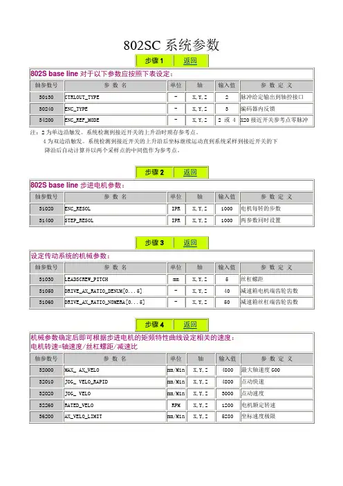
注:2为单边沿触发。
系统检测到接近开关的上升沿时琐存参考点。
4为双边沿触发。
系统检测到接近开关的上升沿后坐标继续运动直到系统采样到接近开关的下降沿后自动计算并以两个采样点的中间值作为参考点。
802S base line的步进电机
系统的另一独特的功能是对坐标的动态特性进行优化。
利用点动方式测试进给轴的动态特性,设定各坐标的最高速度,并选择合适的加速度曲线。
注意: 电机每转脉冲数的容差应考虑到接近开关两个沿的位置差以及在最高进给速度时的跟随误差 丝杠每转步进电机的脉冲数=电机每转的步数 / 减速比
跟随误差对应的脉冲数=丝杠每转步进电机的步数× 最高速度下跟随误差 / 丝杠螺距
802C系统参数
注意:该参数为由611U的WSG接口引出的编码器信号脉冲数。
脉冲数=电机的极对数*1024 比如:电机1FK6060-6AF71-1Sxx,为6极电机,极对数为3;
电机1FK6101-8AF71-1Sxx,为8极电机,极对数为4;
电机1FK7060-5AF71-1Txx,为2极电机,极对数为1;
电机1FK7060-5AF71-1Sxx,为8极电机,极对数为4;。
SIEMENS_802S仿真操作说明书要点
,警告被取消,
可继续进行回零操作。
图 4ቤተ መጻሕፍቲ ባይዱ1
5、定义毛坯
点击菜单栏中“”定义毛坯
点击菜单栏中的“夹具”
,选择零件,选择夹具平口钳,点击向上移动按钮,把
零件调到合适的位置。如图 5-1 所示。
图 5-1
点击菜单栏中的“放置零件”
,选中 定义的毛坯,点击安装零件 。
点击箭头可以调整零件的位置。点击退出。
主菜单工具栏上的
进行选择。
对刀前的准备: 创建刀具。具体过程如下:
点击操作面板上的
按钮,出现如下的界面,如图 7-1。
图 7-1
依次点击软键
、
7-2 所示的对话框:
、按钮
、及软键
。弹出如图
图 7-2
在“ T- 号”栏中输入刀具号 1。点击
按钮,光标移到“ T- 型”栏中,输入刀具类型
100。按软键“确认”。完成新刀具的建立,此时进入参数设置界面:点击
按钮,光标
移到“半径”栏中,输入刀具半径 4。点击回车
。如图 7-3
X 、 Y 轴对刀
图 7-3
铣床在 X , Y 方向对刀时一般使用的是基准工具。基准工具包括“刚性靠棒”和“寻 边器”两种。
注:本使用手册铣床和加工中心对刀时采用的是将零件放置在基准工具的左侧(正面 视图)的方法。
点击菜单栏中的“机床 /基准工具 …”,弹出的基准工具对话框中,左边的是刚性靠棒, 右边的是寻边器。如图 7-4
SIEMENS 802S 系统面板
SIEMENS 802S 面板介绍
按钮
名称
紧急停止
点动距离选择按 钮 手动方式
功
能
简
介
按下急停按钮,使机床移动立即停止,并且所 有的输出如主轴的转动等都会关闭
SINUMERIK 802S 802C 数控仿真控制系统用户手册
目录
概 述 .............................................................................................................................................. 5 SINUMERIK 802S/802C 仿真操作面板 OP ................................................................................ 6 机床控制面板................................................................................................................................... 7 第一篇 SINUMERIK 802 S / C 数控仿真控制系统软件(车床)........................................... 8
2.1 屏幕划分 .................................
802Dsl_NC_PARAMETER参数
802D参数的保护级、口令及生效条件
802D调试培训 802系统的保护级:
1. 2. 3. 专家级(口令:SUNRISE )- 只有在必要时使用 制造商级(口令:EVENING )- 更改标准机床参数 用户级(口令:CUSTOMER)- 浏览机床参数但不能修改
4~7 PLC 保护级
机床参数的生效等级
Page:
1
March, 2005
Automation and Drives - Motion control
SINUMERIK 802D sl – Connecting up
802D调试培训
键盘
24VDC
PP 72/48
操作站 802D PCU
24 VDC 220 VAC
N
PE
RS232隔离器
个人 计算机
© SIEMENS Ltd China
SINUMERIK 802D solution line - Innovative Pruducts
Page:
13
March, 2005
Automation and Drives - Motion control
802D参数设定 – 反向间隙与软限位
802D调试培训
© S solution line - Innovative Pruducts
Page:
14
March, 2005
Automation and Drives - Motion control
丝杠螺距误差补偿 - 误差分析
坐标位置 螺距 x 2 误差 螺距 x 1.5 螺距 x 1 误差 螺距 x 0.5 补偿角 补偿角 补偿角 补偿角 丝杠转角 0º 720º 180º 360º 540º 0.5螺距实际转角 1.0螺距实际转角 1.5螺距实际转角 2.0螺距实际转角
Siemens802S使用说明
第七章 Siemens802S(C)系统7.1 机床操作2134561011121314151. 复位2. 暂停3. 执行4. 点动距离(0.001,0.01,0.1,1,10mm)5. 手动6. 回零7. 自动8. 执行单行指令9. MDA10.主轴反、停、转动(手动时)11.手动移动,加速配合12.进给倍率13.转速倍率14.手轮15.紧急停止879Siemens802S(C)铣、车床、加工中心操作面板7.1.1机床回零1) 松开紧急停止按钮,按复位键开机床。
2) 使手动按钮和回零按钮呈按下状态3) 对X 回零,按住,直到X 坐标为零,界面上X 位置出现回零灯,若中途松开按钮,会出现警告框,此时按复位取消警告,可继续进行操作。
同样对Y 、Z 回零。
4) 按使主轴回零7.1.2自动加工1)先将机床回零。
(参见7.1.1) 2)选择一数控程序。
(参见7.3.2) 3)设置参数(参见7.2) 4)在控制面板上点击,进入自动加工模式。
5) 通过执行、暂停命令来控制程序的运行、停止。
同时状态栏也随之变化。
6) 在自动加工时,如果点击切换机床进入手动模式,将出现警告框,此时按可取消警告,继续操作。
7)也可以按进入单行执行状态,每按一次,执行一行程序。
8)按复位键可使程序重置。
7.1.3 手动/连续加工1)点击切换机床进入手动模式。
2)移动按钮可向相应方向调节机床位置。
3)点击机床主轴手工控制按钮,来控制主轴的转动、停止。
7.1.4 手动/单步加工1)在手动/连续加工时(参见7.1.3“手动/连续加工”)或在对基准时(参见3.4“对基准”),需精确调节机床,可采用单步方式。
2)连续点击单步点动按钮,可在点动距离0.001毫米,0.01毫米,0.1毫米,1毫米,间切换,同样也是配合移动按钮来移动机床进行微调,使其达到要求的位置。
3)用软键“手轮方式”改变手轮移动的轴,点击或按住手轮使机床移动。
4)点击机床主轴手工控制按钮,来控制主轴的转动、停止。
- 1、下载文档前请自行甄别文档内容的完整性,平台不提供额外的编辑、内容补充、找答案等附加服务。
- 2、"仅部分预览"的文档,不可在线预览部分如存在完整性等问题,可反馈申请退款(可完整预览的文档不适用该条件!)。
- 3、如文档侵犯您的权益,请联系客服反馈,我们会尽快为您处理(人工客服工作时间:9:00-18:30)。
1/32April 2006STM690, STM704, STM795STM802, STM804, STM805, STM8063V Supervisor with Battery Switchover* Contact local ST sales office for availability.Rev 7FEATURES SUMMARY■■NVRAM SUPERVISOR FOR EXTERNAL LPSRAM■CHIP-ENABLE GATING (STM795 only) FOR EXTERNAL LPSRAM (7ns max PROP DELAY)■MANUAL (PUSH-BUTTON) RESET INPUT ■200ms (TYP) t rec■WATCHDOG TIMER - 1.6sec (TYP)■AUTOMATIC BATTERY SWITCHOVER■LOW BATTERY SUPPLY CURRENT - 0.4µA (TYP)■POWER-FAIL COMPARATOR (PFI/PFO)■LOW SUPPLY CURRENT - 40µA (TYP)■GUARANTEED RST (RST) ASSERTION DOWN TO V CC = 1.0V■OPERATING TEMPERATURE:–40°C to 85°C (Industrial Grade)Table 1. Device OptionsNote: 1.2.Open drain output.Watchdog InputActive- Low RST (1)Active- High RSTManual Reset Input Battery Switch-overPower-fail Compar-atorChip-Enable GatingSTM690T/S/R ✔✔✔✔STM704T/S/R ✔✔✔✔STM795T/S/R ✔(2)✔✔STM802T/S/R ✔✔✔✔STM804T/S/R ✔✔(2)✔✔STM805T/S/R ✔✔(2)✔✔STM806T/S/R✔✔✔✔STM690/704/795/802/804/805/806TABLE OF CONTENTSFEATURES SUMMARY . . . . . . . . . . . . . . . . . . . . . . . . . . . . . . . . . . . . . . . . . . . . . . . . . . . . . . . . . . . . .1Figure 1.Packages. . . . . . . . . . . . . . . . . . . . . . . . . . . . . . . . . . . . . . . . . . . . . . . . . . . . . . . . . . . . . .1 Table 1.Device Options . . . . . . . . . . . . . . . . . . . . . . . . . . . . . . . . . . . . . . . . . . . . . . . . . . . . . . . . .1SUMMARY DESCRIPTION. . . . . . . . . . . . . . . . . . . . . . . . . . . . . . . . . . . . . . . . . . . . . . . . . . . . . . . . . . .4Figure 2.Logic Diagram (STM690/802/804/805) . . . . . . . . . . . . . . . . . . . . . . . . . . . . . . . . . . . . . . .4 Figure 3.Logic Diagram (STM704/806) . . . . . . . . . . . . . . . . . . . . . . . . . . . . . . . . . . . . . . . . . . . . . .4 Figure 4.Logic Diagram (STM795). . . . . . . . . . . . . . . . . . . . . . . . . . . . . . . . . . . . . . . . . . . . . . . . . .4 Table 2.Signal Names . . . . . . . . . . . . . . . . . . . . . . . . . . . . . . . . . . . . . . . . . . . . . . . . . . . . . . . . . .4 Figure 5.STM690/802/804/805 Connections. . . . . . . . . . . . . . . . . . . . . . . . . . . . . . . . . . . . . . . . . .5 Figure 6.STM704/806 Connections. . . . . . . . . . . . . . . . . . . . . . . . . . . . . . . . . . . . . . . . . . . . . . . . .5 Figure 7.STM795 Connections . . . . . . . . . . . . . . . . . . . . . . . . . . . . . . . . . . . . . . . . . . . . . . . . . . . .5 Pin Descriptions . . . . . . . . . . . . . . . . . . . . . . . . . . . . . . . . . . . . . . . . . . . . . . . . . . . . . . . . . . . . . . .6 Table 3.Pin Description. . . . . . . . . . . . . . . . . . . . . . . . . . . . . . . . . . . . . . . . . . . . . . . . . . . . . . . . . .6 Figure 8.Block Diagram (STM690/802/804/805). . . . . . . . . . . . . . . . . . . . . . . . . . . . . . . . . . . . . . .7 Figure 9.Block Diagram (STM704/806). . . . . . . . . . . . . . . . . . . . . . . . . . . . . . . . . . . . . . . . . . . . . .7 Figure 10.Block Diagram (STM795) . . . . . . . . . . . . . . . . . . . . . . . . . . . . . . . . . . . . . . . . . . . . . . . . .8 Figure 11.Hardware Hookup. . . . . . . . . . . . . . . . . . . . . . . . . . . . . . . . . . . . . . . . . . . . . . . . . . . . . . .8OPERATION . . . . . . . . . . . . . . . . . . . . . . . . . . . . . . . . . . . . . . . . . . . . . . . . . . . . . . . . . . . . . . . . . . . . . .9Reset Output . . . . . . . . . . . . . . . . . . . . . . . . . . . . . . . . . . . . . . . . . . . . . . . . . . . . . . . . . . . . . . . . . .9 Push-button Reset Input (STM704/806). . . . . . . . . . . . . . . . . . . . . . . . . . . . . . . . . . . . . . . . . . . . .9 Watchdog Input (NOT available on STM704/795/806) . . . . . . . . . . . . . . . . . . . . . . . . . . . . . . . . .9 Back-up Battery Switchover. . . . . . . . . . . . . . . . . . . . . . . . . . . . . . . . . . . . . . . . . . . . . . . . . . . . . .9 Table 4.I/O Status in Battery Back-up . . . . . . . . . . . . . . . . . . . . . . . . . . . . . . . . . . . . . . . . . . . . ..9 Chip-Enable Gating (STM795 only) . . . . . . . . . . . . . . . . . . . . . . . . . . . . . . . . . . . . . . . . . . . . . . .10 Chip Enable Input (STM795 only). . . . . . . . . . . . . . . . . . . . . . . . . . . . . . . . . . . . . . . . . . . . . . . . .10 Chip Enable Output (STM795 only) . . . . . . . . . . . . . . . . . . . . . . . . . . . . . . . . . . . . . . . . . . . . . . .10 Figure 12.Chip-Enable Gating. . . . . . . . . . . . . . . . . . . . . . . . . . . . . . . . . . . . . . . . . . . . . . . . . . . . .10 Figure 13.Chip Enable Waveform (STM795) . . . . . . . . . . . . . . . . . . . . . . . . . . . . . . . . . . . . . . . . .10 Power-fail Input/Output (NOT available on STM795) . . . . . . . . . . . . . . . . . . . . . . . . . . . . . . . . .11 Applications Information . . . . . . . . . . . . . . . . . . . . . . . . . . . . . . . . . . . . . . . . . . . . . . . . . . . . . . .11 Figure 14.Power-fail Comparator Waveform (STM690/704/802/804/805/806). . . . . . . . . . . . . . . .11 Using a SuperCap™ as a Backup Power Source. . . . . . . . . . . . . . . . . . . . . . . . . . . . . . . . . . . .12 Figure ing a SuperCap™. . . . . . . . . . . . . . . . . . . . . . . . . . . . . . . . . . . . . . . . . . . . . . . . . . . .12 Negative-Going V CC Transients. . . . . . . . . . . . . . . . . . . . . . . . . . . . . . . . . . . . . . . . . . . . . . . . . .12TYPICAL OPERATING CHARACTERISTICS . . . . . . . . . . . . . . . . . . . . . . . . . . . . . . . . . . . . . . . . . . .13Figure 16.V CC-to-V OUT On-Resistance vs. Temperature . . . . . . . . . . . . . . . . . . . . . . . . . . . . . . . .13 Figure 17.V BAT-to-V OUT On-Resistance vs. Temperature. . . . . . . . . . . . . . . . . . . . . . . . . . . . . . . .13 Figure 18.Supply Current vs. Temperature (no load) . . . . . . . . . . . . . . . . . . . . . . . . . . . . . . . . . . .14 Figure 19.Battery Current vs. Temperature. . . . . . . . . . . . . . . . . . . . . . . . . . . . . . . . . . . . . . . . . . .14 Figure 20.V PFI Threshold vs. Temperature. . . . . . . . . . . . . . . . . . . . . . . . . . . . . . . . . . . . . . . . . . .152/32STM690/704/795/802/804/805/806Figure 21.Reset Comparator Propagation Delay vs. Temperature. . . . . . . . . . . . . . . . . . . . . . . . .15 Figure 22.Power-up t rec vs. Temperature . . . . . . . . . . . . . . . . . . . . . . . . . . . . . . . . . . . . . . . . . . . .16 Figure 23.Normalized Reset Threshold vs. Temperature . . . . . . . . . . . . . . . . . . . . . . . . . . . . . . . .16 Figure 24.Watchdog Time-out Period vs. Temperature . . . . . . . . . . . . . . . . . . . . . . . . . . . . . . . . .17 Figure 25.E to E CON On-Resistance vs. Temperature . . . . . . . . . . . . . . . . . . . . . . . . . . . . . . . . . .1718 Figure 27.Output Voltage vs. Load Current (V CC = 5V; V BAT = 2.8V; T A = 25°C). . . . . . . . . . . . . .18 Figure 28.Output Voltage vs. Load Current (V CC = 0V; V BAT = 2.8V; T A = 25°C). . . . . . . . . . . . . .19 Figure 29.RST Output Voltage vs. Supply Voltage. . . . . . . . . . . . . . . . . . . . . . . . . . . . . . . . . . . . .19 Figure 30.RST Output Voltage vs. Supply Voltage. . . . . . . . . . . . . . . . . . . . . . . . . . . . . . . . . . . . .20 Figure 31.Power-fail Comparator Response Time (Assertion) . . . . . . . . . . . . . . . . . . . . . . . . . . . .20 Figure 32.Power-fail Comparator Response Time (De-Assertion) . . . . . . . . . . . . . . . . . . . . . . . . .21 Figure 33.Maximum Transient Duration vs. Reset Threshold Overdrive. . . . . . . . . . . . . . . . . . . . .21 CON Propagation Delay vs. Temperature . . . . . . . . . . . . . . . . . . . . . . . . . . . . . . .22MAXIMUM RATING. . . . . . . . . . . . . . . . . . . . . . . . . . . . . . . . . . . . . . . . . . . . . . . . . . . . . . . . . . . . . . . .22 Table 5.Absolute Maximum Ratings. . . . . . . . . . . . . . . . . . . . . . . . . . . . . . . . . . . . . . . . . . . . . . .22DC and AC PARAMETERS . . . . . . . . . . . . . . . . . . . . . . . . . . . . . . . . . . . . . . . . . . . . . . . . . . . . . . . . .23Table 6.Operating and AC Measurement Conditions. . . . . . . . . . . . . . . . . . . . . . . . . . . . . . . . . .2323 Figure 36.AC Testing Input/Output Waveforms. . . . . . . . . . . . . . . . . . . . . . . . . . . . . . . . . . . . . . . .23 Figure 37.MR Timing Waveform . . . . . . . . . . . . . . . . . . . . . . . . . . . . . . . . . . . . . . . . . . . . . . . . . . .24 Figure 38.Watchdog Timing . . . . . . . . . . . . . . . . . . . . . . . . . . . . . . . . . . . . . . . . . . . . . . . . . . . . . .24 Table 7.DC and AC Characteristics . . . . . . . . . . . . . . . . . . . . . . . . . . . . . . . . . . . . . . . . . . . . . . .24PACKAGE MECHANICAL . . . . . . . . . . . . . . . . . . . . . . . . . . . . . . . . . . . . . . . . . . . . . . . . . . . . . . . . . .27Figure 39.SO8 – 8-lead Plastic Small Outline, 150 mils body width, Package Mech. Drawing. . . .27 Table 8.SO8 – 8-lead Plastic Small Outline, 150 mils body width, Package Mechanical Data . .27 Figure 40.TSSOP8 – 8-lead, Thin Shrink Small Outline, 3x3mm body size, Outline . . . . . . . . . . .28 Table 9.TSSOP8 – 8-lead, Thin Shrink Small Outline, 3x3mm body size, Mechanical Data. . . .28PART NUMBERING . . . . . . . . . . . . . . . . . . . . . . . . . . . . . . . . . . . . . . . . . . . . . . . . . . . . . . . . . . . . . . .29Table 10.Ordering Information Scheme . . . . . . . . . . . . . . . . . . . . . . . . . . . . . . . . . . . . . . . . . . . . .29 Table 11.Marking Description. . . . . . . . . . . . . . . . . . . . . . . . . . . . . . . . . . . . . . . . . . . . . . . . . . . . .30REVISION HISTORY. . . . . . . . . . . . . . . . . . . . . . . . . . . . . . . . . . . . . . . . . . . . . . . . . . . . . . . . . . . . . . .31 Table 12.Document Revision History. . . . . . . . . . . . . . . . . . . . . . . . . . . . . . . . . . . . . . . . . . . . . . .313/32STM690/704/795/802/804/805/8064/32SUMMARY DESCRIPTIONThe STM690/704/795/802/804/805/806 Supervi-sors are self-contained devices which provide mi-croprocessor supervisory functions with the ability to non-volatize and write-protect external LPSRAM. A precision voltage reference and com-parator monitors the V CC input for an out-of-toler-ance condition. When an invalid V CC condition occurs, the reset output (RST) is forced low (or high in the case of RST). These devices also offer a watchdog timer (except for STM704/795/806) as well as a power-fail comparator (except for STM795) to provide the system with an early warning of impending power failure.These devices are available in a standard 8-pin SOIC package or a space-saving 8-pin TSSOP package.Note: 1.For STM804/805, reset output is active-high and opendrain.Table 2. Signal NamesNote: 1.Open drain for STM804/805 only.2.STM795MR Push-button Reset Input WDIWatchdog InputRST Active-Low Reset Output RST (1)Active-High Reset Output E (2)Chip Enable InputE CON (2)Conditioned Chip Enable Output Vccsw (2)V CC Switch Output V OUTSupply Voltage Output V CC Supply Voltage V BAT Back-up Supply Voltage PFI Power-fail Input PFO Power-fail Output V SSGroundSTM690/704/795/802/804/805/806drain.5/32STM690/704/795/802/804/805/8066/32Pin DescriptionsMR (Manual Reset).A logic low on /MR assertsthe reset output. Reset remains asserted as long as MR is low and for t rec after MR returns high.This active-low input has an internal pull-up. It can be driven from a TTL or CMOS logic line, or short-ed to ground with a switch. Leave open if unused.WDI (Watchdog Input).If WDI remains high orlow for 1.6sec, the internal watchdog timer runsout and reset is triggered. The internal watchdogtimer clears while reset is asserted or when WDIsees a rising or falling edge.The watchdog function cannot be disabled by al-lowing the WDI pin to float.Pulses low for t recwhen triggered, and stays low whenever V CC islow. It remains low for t rec after either V CC risesabove the reset threshold, the watchdog triggers areset, or MR goes from low to high.RST (Active-high Reset - Open Drain).Pulseshigh for t rec when triggered, and stays high when-ever V CC is above the reset threshold or when MRis a logic high. It remains high for t rec after eitherV CC falls below the reset threshold, the watchdogtriggers a reset, or MR goes from high to low.PFI (Power-fail Input).When PFI is less thanV PFI or when V CC falls below V SW to ground if unused.PFO (Power-fail Output).When PFI is less than V PFI , or V CC falls below V SW , PFO goes low; oth-erwise, PFO remains high. Leave open if unused.V OUT (Supply Output Voltage).When V CC is above the switchover voltage (V SO ), V OUT is con-nected to V CC through a P-channel MOSFET switch. When V CC falls below V SO , V BAT connects to V OUT . Connect to V CC if no battery is Switch Output).When V OUT switches to battery, Vccsw is high. When V OUT switches back to V CC to drive gate of external PMOS transistor for I OUT requirements exceeding 75mA.The input to the chip-en-able gating circuit. Connect to ground if unused.E CON (Conditional Chip Enable).E CON goes low only when E is low and reset is not asserted. If E CON is low when reset is asserted, E CON will re-main low for 15µs or until E goes high, whichever occurs first. In the disabled mode, E CON is pulled up to V OUT .V BAT (Back-up Battery Input).When V CC falls below V SO , V OUT switches from V CC to V BAT .When V CC rises above V SO + hysteresis, V OUT re-connects to V CC . V BAT may exceed V CC . Connect to V CC if no battery is used.Table 3. Pin DescriptionPinNameFunctionSTM795STM690STM802STM704STM806STM804STM805––6–MR Push-button Reset Input –6–6WDI Watchdog Input777–RST Active-Low Reset Output –––7RST Active-High ResetOutput –444PFI Power-failInput –555PFO Power-fail Output1111V OUT Supply Output for External LPSRAM 2222V CC Supply Voltage 3–––Vccsw V CC Switch Output 4333V SS Ground5–––E Chip Enable Input6–––E CON Conditioned Chip Enable Output 8888V BATBackup-Battery InputSTM690/704/795/802/804/805/806Note: 1.For STM804/805, reset output is active-high and open drain.7/32STM690/704/795/802/804/805/806Note: 1.For STM690/802/804/805.2.For STM795 only.3.Not available on STM795.4.For STM704/806.8/32STM690/704/795/802/804/805/806 OPERATIONReset OutputThe STM690/704/795/802/804/805/806 Supervi-sor asserts a reset signal to the MCU whenever V CC goes below the reset threshold (V RST), a watchdog time-out occurs, or when the Push-but-teed to be a logic low (logic high for STM804/805) for 0V < V CC < V RST if V BAT is greater than 1V. id down to V CC =1V.During power-up, once V CC exceeds the reset threshold an internal timer keeps RST low for the reset time-out period, t recreturns high.If V CC drops below the reset threshold, RST goes low. Each time RST is asserted, it stays low for at least the reset time-out period (t rec). Any time V CC goes below the reset threshold the internal timer clears. The reset timer starts when V CC returns above the reset threshold.Push-button Reset Input (STM704/806)A logic low on MR asserts reset. Reset remainsrec (see Figure 37.,page24) after it returns high. The MR input has an internal 40kΩ pull-up resistor, allowing it to be left open if not used. This input can be driven with TTL/CMOS-logic levels or with open-drain/ collector outputs. Connect a normally open mo-mentary switch from MR to GND to create a man-ual reset function; external debounce circuitry is not required. If MR is driven from long cables or the device is used in a noisy environment, connect a 0.1µF capacitor from MR to GND to provide ad-ditional noise immunity. MR may float, or be tied to V CC when not used.Watchdog Input (NOT available on STM704/ 795/806)The watchdog timer can be used to detect an out-of-control MCU. If the MCU does not toggle the Watchdog Input (WDI) within t WD (1.6sec typ), the reset is asserted. The internal watchdog timer is cleared by either:1. a reset pulse, or2.by toggling WDI (high-to-low or low-to-high),which can detect pulses as short as 50ns. If WDI is tied high or low, a reset pulse istriggered every 1.8sec (t WD + t rec).The timer remains cleared and does not count for as long as reset is asserted. As soon as reset is re-leased, the timer starts counting (see Figure 38.,page24).Note: Input frequency greater than 20ns (50MHz) will be filtered.Back-up Battery SwitchoverIn the event of a power failure, it may be necessary to preserve the contents of external SRAM through V OUT. With a backup battery installed with voltage V BAT, the devices automatically switch the SRAM to the back-up supply when V CC falls. Note: If back-up battery is not used, connect both V BAT and V OUT to V CC.This family of Supervisors does not always con-nect V BAT to V OUT when V BAT is greater than V CC. V BAT connects to V OUT (through a 100Ω switch) when V CC is below V SW (2.4V) or V BAT (whichever is lower). This is done to allow the back-up battery (e.g., a 3.6V lithium cell) to have a higher voltage than V CC.Assuming that V BAT > 2.0V, switchover at V SO en-sures that battery back-up mode is entered before V OUT gets too close to the 2.0V minimum required to reliably retain data in most external SRAMs. When V CC recovers, hysteresis is used to avoid oscillation around the V SO point. V OUT is connect-ed to V CC through a 3Ω PMOS power switch. Note: The back-up battery may be removed while V CC is valid, assuming V BAT is adequately decou-pled (0.1µF typ), without danger of triggering a re-set.Table 4. I/O Status in Battery Back-up Pin StatusV OUT Connected to V BAT through internal switchV CC Disconnected from V OUTPFI DisabledPFO Logic LowE High impedanceE CON Logic HighWDI Watchdog timer is disabledMR DisabledRST Logic LowRST Logic HighV BAT Connected to V OUTVccsw Logic High (STM795)9/32STM690/704/795/802/804/805/80610/32Chip-Enable Gating (STM795 only)vents erroneous data from corrupting the external CMOS RAM in the event of an undervoltage con-dition. The STM795 uses a series transmission CON (see Figure 12). During nor-mal operation (reset not asserted), the E transmis-sion gate is enabled and passes all E transitions.When reset is asserted, this path becomes dis-abled, preventing erroneous data from corrupting the CMOS RAM. The short E propagation delay from E to E CON enables the STM795 to be used with most µPs. If E is low when reset asserts,CON remains low for typically 10µs to permit the current WRITE cycle to complete.Chip Enable Input (STM795 only)The chip-enable transmission gate is disabled and is asserted. During a power-down sequence when V CC passes the reset threshold, the chip-enable transmission gate disables and E immediately be-comes high impedance if the voltage at E is high.If E is low when reset asserts, the chip-enable transmission gate will disable 10µs after reset as-serts (see Figure 13). This permits the current WRITE cycle to complete during power-down.Any time a reset is generated, the chip-enable transmission gate remains disabled and E remains first half of the reset time-out period (t rec /2). When the chip enable transmission gate is enabled, the impedance of E appears as a 40Ω resistor in se-ries with the load at E CON . The propagation delay through the chip-enable transmission gate de-pends on V CC , the source impedance of the drive connected to E, and the loading on E CON . The chip enable propagation delay is production tested from the 50% point on E to the 50% point on E CON using a 50Ω driver and a 50pF load capacitance (see Figure 36.,page 23). For minimum propaga-CON and use a low-output impedance driver.Chip Enable Output (STM795 only)When the chip-enable transmission gate is en-CON is equivalent to a 40Ωthe disabled mode, the transmission gate is off and an active pull-up connects E CON to V OUT (see Figure 12). This pull-up turns off when the trans-mission gate is enabled.Power-fail Input/Output (NOT available on STM795)The Power-fail Input (PFI) is compared to an inter-nal reference voltage (independent from the V RST comparator). If PFI is less than the power-fail threshold (V PFI), the Power-Fail Output (PFO) will go low. This function is intended for use as an un-dervoltage detector to signal a failing power sup-ply. Typically PFI is connected through an external voltage divider (see Figure 11.,page8) to either the unregulated DC input (if it is available) or the regulated output of the V CC regulator. The voltage divider can be set up such that the voltage at PFI falls below V PFI several milliseconds before the regulated V CC input to the STM690/704/795/802/ 804/805/806 or the microprocessor drops below the minimum operating voltage.During battery back-up, the power-fail comparator Figure 14.,page11). This occurs after V CC drops below V SW (2.4V). When power returns, the pow-If the comparator is unused, PFI should be con-nected to V SS and PFO left unconnected. PFO may be connected to MR on the STM704/806 so that a low voltage on PFI will generate a reset out-put.Applications InformationThese Supervisor circuits are not short-circuit pro-tected. Shorting V OUT to ground - excluding pow-er-up transients such as charging a decoupling capacitor - destroys the device. Decouple both V CC and V BAT pins to ground by placing 0.1µF ca-pacitors as close to the device as possible.11/32Using a SuperCap™ as a Backup Power SourceSuperCaps™ are capacitors with extremely high capacitance values (e.g., order of 0.47F) for their size. Figure 15 shows how to use a SuperCap as a back-up power source. The SuperCap may be connected through a diode to the V CC supply. Since V BAT can exceed V CC while V CC is above the reset threshold, there are no special precau-tions when using these supervisors with a Super-Cap.Negative-Going V CC TransientsThe STM690/704/795/802/804/805/806 Supervi-sors are relatively immune to negative-going V CC transients (glitches). Figure 33.,page21 was gen-erated using a negative pulse applied to V CC, starting at V RST + 0.3V and ending below the reset threshold by the magnitude indicated (comparator overdrive). The graph indicates the maximum pulse width a negative V CC transient can have without causing a reset pulse. As the magnitude of the transient increases (further below the thresh-old), the maximum allowable pulse width decreas-es. Any combination of duration and overdrive which lies under the curve will NOT generate a re-set signal. Typically, a V CC transient that goes 100mV below the reset threshold and lasts 40µs or less will not cause a reset pulse. A 0.1µF bypass capacitor mounted as close as possible to the V CC pin provides additional transient immunity.12/32TYPICAL OPERATING CHARACTERISTICSNote: Typical values are at T A = 25°C.13/3214/3215/3216/32Figure 25. E to E17/32Figure 26. PFI to PFO Propagation Delay vs. Temperature18/32Figure 29. RST Output Voltage vs. Supply Voltage19/32500ns/divAI09153b20/32Figure 33. Maximum Transient Duration vs. Reset Threshold Overdrive AI09154b500ns/div21/3222/32Figure 34. E to E MAXIMUM RATINGStressing the device above the rating listed in the Absolute Maximum Ratings” table may cause per-manent damage to the device. These are stress ratings only and operation of the device at these or any other conditions above those indicated in the Operating sections of this specification is not im-plied. Exposure to Absolute Maximum Rating con-ditions for extended periods may affect device reliability. Refer also to the STMicroelectronics SURE Program and other relevant quality docu-ments.Table 5. Absolute Maximum RatingsNote: 1.Reflow at peak temperature of 255°C to 260°C for < 30 seconds (total thermal budget not to exceed 180°C for between 90 to 150seconds).Symbol ParameterValue Unit T STG Storage Temperature (V CC Off)–55 to 150°C T SLD (1)Lead Solder Temperature for 10 seconds 260°C V IO Input or Output Voltage –0.3 to V CC +0.3V V CC /V BATSupply Voltage –0.3 to 6.0V I O Output Current 20mA P DPower Dissipation320mW23/32DC AND AC PARAMETERSThis section summarizes the operating measure-ment conditions, and the DC and AC characteris-tics of the device. The parameters in the DC and AC characteristics Tables that follow, are derived from tests performed under the MeasurementConditions summarized in Table 6, Operating and AC Measurement Conditions. Designers should check that the operating conditions in their circuit match the operating conditions when relying on the quoted parameters.Table 6. Operating and AC Measurement ConditionsFigure 35. E to E Note: 1.C L includes load capacitance and scope probe capacitance.ParameterSTM690/704/795/802/804/805/806Unit V CC /V BAT Supply Voltage1.0 to 5.5V Ambient Operating Temperature (T A )–40 to 85°C Input Rise and Fall Times ≤5ns Input Pulse Voltages0.2 to 0.8V CC V Input and Output Timing Ref. Voltages0.3 to 0.7V CCVFigure 37. MR Timing Waveform Note: 1.RST for STM805.Table 7. DC and AC CharacteristicsSym Alter-nativeDescription Test Condition(1)Min Typ Max UnitV CC,V BAT(2)Operating Voltage T A = –40 to +85°C 1.1(3) 5.5VI CC V CC Supply CurrentExcluding I OUT (V CC < 5.5V)4060µAExcluding I OUT (V CC < 3.6V)3550µA V CC Supply Current inBattery Back-up ModeExcluding I OUT(V BAT = 2.3V,V CC = 2.0V, MR = V CC)2535µAI BAT(4)V BAT Supply Current inBattery Back-up ModeExcluding I OUT(V BAT = 3.6V)0.4 1.0µAV OUT1V OUT Voltage (Active)I OUT1 = 5mA(5)V CC –0.03V CC –0.015V I OUT1 = 75mAV CC –0.3V CC –0.15V I OUT1 = 250µA,V CC > 2.5V(5)V CC –0.0015V CC –0.0006VV OUT2V OUT Voltage (BatteryBack-up)I OUT2 = 250µA, V BAT = 2.3VV BAT –0.1V BAT –0.034VI OUT2 = 1mA, V BAT = 2.3VV BAT –0.14V V CC to V OUT On-resistance34ΩV BAT to V OUT On-resistance100Ω24/32I LI Input Leakage Current (MR)STM704/806 only;MR = 0V, V CC = 3V2075350µA Input Leakage Current (PFI)0V = V IN = V CC–252+25nA Input Leakage Current (WDI)0V = V IN = V CC–1+1µAI LO Output Leakage Current STM804/805/795;0V = V IN = V CC(6)–1+1µAV IH Input High Voltage (MR, WDI)V RST (max) < V CC < 5.5V0.7V CC V V IL Input Low Voltage (MR, WDI)V RST (max) < V CC < 5.5V0.3V CC VV OL Output Low Voltage (PFO,RST, RST, Vccsw)V CC = V RST (max),I SINK = 3.2mA0.3V Output Low Voltage (E CON)V CC = V RST (max),I OUT = 1.6mA, E = 0V0.2V CC VV OL Output Low Voltage (RST)I OL = 40µA,V CC = 1.0V, V BAT = V CC,T A = 0°C to 85°C0.3VI OL = 200µA,V CC = 1.2V, V BAT = V CC0.3VV OH Output High Voltage (RST,RST)(7)I SOURCE = 1mA,V CC = V RST (max)2.4V Output High Voltage (E CON)V CC = V RST (max),I OUT = 1.6mA, E = V CC0.8V CC V Output High Voltage (PFO)I SOURCE = 75µA,V CC = V RST (max)0.8V CC VV OHB V OH Battery Back-up (Vccsw,RST)I SOURCE = 100µA,V CC = 0V, V BAT = 2.8V0.8V BA T V V OH Battery Back-up (E CON)I SOURCE = 75µA,V CC = 0V, V BAT = 2.8V0.8V BA T VPower-fail Comparator (NOT available on STM795)V PFI PFI Input ThresholdPFI Falling(V CC < 3.6V)STM802/804/8061.212 1.237 1.262VSTM690/704/8051.187 1.237 1.287VPFI Hysteresis PFI Rising (V CC < 3.6V)1020mV t PFD PFI to PFO PropagationDelay2µsI SC PFO Output Short toGND CurrentV CC = 3.6V, PFO = 0V0.10.75 2.0mABattery SwitchoverV SOBattery Back-upSwitchover Voltage (8,9)Power-downV BA T > V SW V SW VV BA T < V SW V BA T VPower-upV BA T > V SW V SW VV BA T < V SW V BA T V V SW 2.4V Hysteresis40mVSym Alter-nativeDescription Test Condition(1)Min Typ Max Unit25/32。