FDLL4150_NL中文资料
士兰微电子LED照明驱动产品及方案-FC

R22 U3 R23
D5
page13
Silan 士兰微电子
AC-DC LED Lighting Solutions AC-DC LED 照明驱动产品及方案
SD7530 功率因数校正控制器
关键参数列表
典型参数 VCC极限电压值 VCC工作电压最大值 VCC开启电压值 VCC关闭电压值 VCC过压保护值 IC启动电流 原边OCP比较点 输入UVLO 输入OVP GATE钳位电压 短路保护
Silan 士兰微电子
DC-DC LED 照明驱动产品及方案
Company Confidential, don’t copy
Silan 士兰微电子
DC-DC LED 照明驱动产品及方案
型号 SD42522 SD42524 SD42525 SD42527 SD42560 SD42565 SD42566 SD42567
SD7530
40V 32V 17V 9V 33.5V 5uA 1.7V 0.95V 4.5V 15V 专利
Company Confidential, don’t copy
page14
Silan 士兰微电子
VCC特性描述
AC-DC LED Lighting Solutions AC-DC LED 照明驱动产品及方案
SILAN LED 照明驱动产品及解决方案
Find what we can do……
Up d 201 ate 2.3
Silan 士兰微电子
LED 照明驱动产品及方案
DC-DC LED 照明驱动产品
◆ SD4252X 系列 -降压型(BUCK) ◆ SD42560 - 升-降压型(BUCK-BOOST) ◆ 80V高压系列(升压SD42566,降压SD42565,升/降压SD42567)
雷达液位计规格书
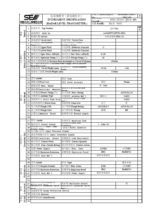
1REV234567891011121314151617181920212223242526272829303132333435363738394041424344454647484950罐旁安装LCD 1/2"NPT 外壳材质 Case Mat'l 铝外壳带涂层指示仪T a n k I n d i c a t o r型号 Model形式 Type显示内容 Display Content 电气接口 Elec. Conn.电源 Power Supply电气接口 Elec. Conn.24VDC 1/2"NPT 防护等级 Enclosure Protection 防爆等级 Explosion ProofIP65ExdIICT4接点形式 Contact Form 接点数量 Contact Quantity 接点容量 Cont. Current Rating 接点作用形式 Contact Action压力输入信号 Input Pressure Signal 油水界面输入信号 Input Interface Signal 辅助输出Auxiliary Output 负载阻抗 Load Resistance 4~20mA DC温度输入信号 Input Temp. Signal Type温度点数Cell Quantity变送单元T r a n s m i t t e r U n i t型号 Model安装形式 Mounting Type 输出信号 Output Signal 总线标准Field Bus Standard法兰材质 Flange Mat'l 法兰密封面 Facing 碳钢RF计量认证Measure Proof 延伸管长度 Extend Length 过程连接形式 Proce.Conn.连接规格 Conn.Size 法兰8"法兰标准 Flange STD 法兰等级 Flange Rating ANSI B16.5ANSI CL150天线形式 Antenna Type 天线材质 Antenna Mat'l 喇叭口316SS 导波管尺寸 Still Pipe Size 导波管材质 Still Pipe Mat'l 316SS 辅助测量Auxiliary Measure 罐底水位量程Interface Range工作温度 Process Temp.(℃)压力等级 Press. Rating ANSI CL150液位±3mm测量范围 Meas. Range0~18m设备法兰高度 Nozzle Height (mm)250mm液位计L e v e l G a u g e型号 Model型式 Type测量功能Function 精度 Level Accuracy法兰面距测量基准点 Distance from Flange Face to Measure Base Point (mm)设备高度 Vessle Height (mm)设备直径 Vessle Diameter (mm)16.5m11m操作温度 Operation Temp.(℃)设计温度 Design Temp.(℃)55雷达与设备壁距离 Distance from Instrument to Vessle Wall(mm)1500mm下部介质 Lower Fluid 介电常数 Dielectric Constant操作压力 Oper. Press. MPa(G)设计压力 Des. Press. MPa(G)0.165工艺条件P r o c e s s C o n d i t i o n s环境温度 Environment Temp.(℃)介质表面状态 Fluid Surface State上部介质 Upper Fluid介电常数 Dielectric Constant 水检测位置 Service 冷焦水储水罐D-132设备材质 Vessle Mat'l 设备等级 Vessle Class(RADAR LEVEL TRANSMITTER )页数 PAGE :第1页 共3页概况G e n e r a l仪表位号 Tag NumberLT-7002流程图号 P&ID No.A10400WS-DW02-0001仪表规格书(雷达液位计)档案号 DOCUMENT No :A10400IN-SP01-1001(16)INSTRUMENT SPECIFICATION 设计阶段 STAGE :详细工程设计版本:AFC IP65ExdIICT4外壳材质 Case Mat'l 供电电源 Power Supply铝外壳带涂层防护等级 Enclosure Protection 防爆等级 Explosion Proof 带隔离阀尺寸 Isolated Valve Size 隔离阀材质 Isolated Valve Mat'l清洗和吹扫接管Clean & Flush Conn.Pipe防护罩 Enclosure Shield安装支架 Bracket其他M i s c e l l推荐制造商 Manufacturer 附 件A c c e s s o r i e s浪涌保护器 Surge Protection Device本表数据未经SEI书面允许不得扩散至第三方1REV2345678910111213141516171819202122232425262728293031323334353637383940414243444546说明 NOTES :带20m连接电缆。
1N4148、1N4150、1N4448 开关二极管
“电子爱好者”网站是一个面向广大电子爱好者、大专院校学生、中小型企业工程技 术人员的电子技术应用、推广专业网站。主要内容有:电子技术应用交流,器件资料、电 子设计软件下载,电子技术支持服务,电子产品发布、转让和引进等信息。
本资料由"电子爱好者"网站收集整理,版权属原作者
The products listed in this document are designed to be used with ordinary electronic equipment or devices (such as audio visual equipment, office-automation equipment, communications devices, electrical appliances and electronic toys). Should you intend to use these products with equipment or devices which require an extremely high level of reliability and the malfunction of with would directly endanger human life (such as medical instruments, transportation equipment, aerospace machinery, nuclear-reactor controllers, fuel controllers and other safety devices), please be sure to consult with our sales representative in advance.
NS4150 用户手册说明书
NS4150用户手册V1.0深圳市纳芯威科技有限公司2011年05月修改历史目录1功能说明 (5)2主要特性 (5)3应用领域 (5)4典型应用电路 (5)5极限参数 (6)6电气特性 (6)7芯片管脚描述 (7)7.1MSOP8和SOP8管脚分配图 (7)7.2管脚功能描述..............................................................................................................................77.3芯片印章说明 (8)8NS4150典型参考特性 (8)9NS4150应用说明 (10)9.1原理框图 (10)9.2工作原理 (11)9.3无需输出滤波器 (11)9.4上电,掉电噪声抑制 (11)9.5EMI增强技术 (11)9.6CTRL引脚设置 (11)9.7效率 (12)9.8保护电路....................................................................................................................................129.9应用信息 (12)10芯片的封装 (13)10.1MSOP-8封装尺寸图 (13)10.2SOP-8封装尺寸图 (14)图目录图1NS4150典型应用图 (5)图2MSOP8和SOP8管脚分配图(top view) (7)图3印章说明 (8)图4NS4150功能框图 (10)图5EMI测试频谱图 (11)图6差分和单端输入方式 (12)图7磁珠与电容 (12)图8MSOP-8封装尺寸图 (13)图9SOP-8封装尺寸图 (14)表目录表1芯片最大物理极限值 (6)表2NS4150电气特性表 (6)表3NS4150管脚描述 (7)表4工作模式 (11)1功能说明NS4150是一款超低EMI、无需滤波器3W单声道D类音频功率放大器。
管网运行状态监测设备
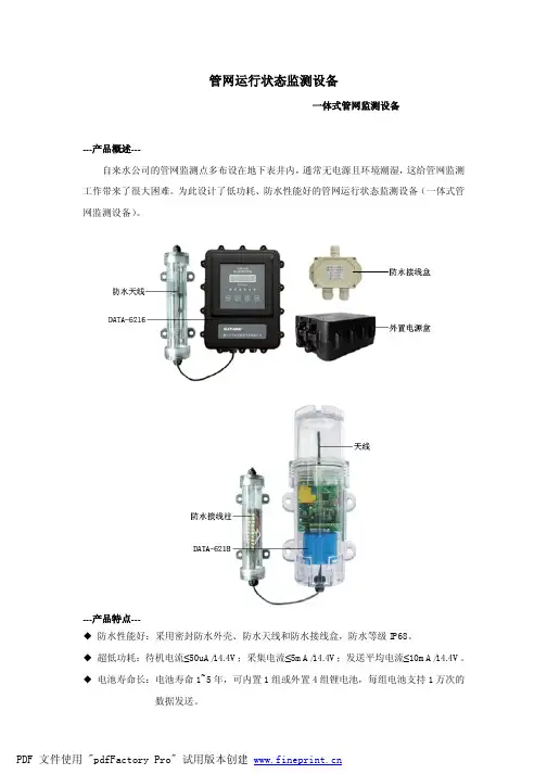
管网运行状态监测设备一体式管网监测设备---产品概述---自来水公司的管网监测点多布设在地下表井内,通常无电源且环境潮湿,这给管网监测工作带来了很大困难。
为此设计了低功耗、防水性能好的管网运行状态监测设备(一体式管网监测设备)。
---产品特点---◆防水性能好:采用密封防水外壳、防水天线和防水接线盒,防水等级IP68。
◆超低功耗:待机电流≤50uA/14.4V;采集电流≤5mA/14.4V;发送平均电流≤10mA/14.4V。
◆电池寿命长:电池寿命1~5年,可内置1组或外置4组锂电池,每组电池支持1万次的数据发送。
◆存储容量大:可存储不少于1年的历史数据。
◆维护方便:可远程设置工作参数、远程升级程序。
◆接入灵活:可接入平升公司配套的上位机系统,也可接入组态软件或用户自行开发的监控软件。
---产品功能---◆采集功能:实时采集压力、流量、水质等数据;采集电池电压。
◆通信功能:采用GPRS或短消息上报数据;支持定时上报、越限报警;支持多中心上报。
◆存储功能:本机循环存储监测数据。
◆显示功能:LCD液晶面板显示当前监测数据和工作参数(DATA-6216型)。
◆对外供电功能:可对外提供5V、12V直流电源,为压力变送器供电。
◆报警功能:压力超限、设备连线中断或电池电压过低时,立即上报告警信息。
---现场安装图片---沈阳市管网监测现场呼和浩特市管网监测现场兰州市管网监测现场唐山市管网监测现场压力变送器防水接线盒一体式管网监测设备DATA-6218 一体式管网监测设备DATA-6216管网运行状态监测设备分体式管网监测设备---产品概述---管网监测现场通常为窨井,存在无电源、环境潮湿、GPRS信号弱等诸多问题,给管网监测带来了很多困难。
分体式管网监测设备采用井下、井上分体安装,433MHZ和GPRS通信互补的方式有效解决了上述难题。
分体式管网监测设备由433M微功耗测控终端和无线数传网关两部分组成,可精确采集安装在地下表井内的流量计/脉冲水表、压力变送器、水位变送器等仪表数据。
slf系列贴片电感datasheet
特点 ●是最适用于电源系统的低直流电阻,大电流,节能型产品。 ●因采用磁力屏蔽结构,所以可实现高密度安装。 ●底面为平直的低背型 , 可稳定地安装在电路板上。 ●采用卷带仕样,支持自动插入机。 用途 手机,计算机,硬盘驱动器,其他各种电子设备 仕样
工作温度范围 保存温度范围 –20 to +85°C [包括自身温度上升] –40 to +85°C [产品单体]
电气特性
电感 (H) 4.7 6.8 10 15 22 33 47 68 100 150 220 电感容差 ±20% ±20% ±20% ±20% ±20% ±20% ±20% ±20% ±20% ±20% ±20% L 测定频率 (kHz) 100 100 100 100 100 100 100 100 100 100 100 直流电阻 ( )±20% 0.0284 0.0354 0.0532 0.0745 0.104 0.148 0.21 0.29 0.43 0.65 0.98 额定电流 (A) 基于电感 变化率时 1.6max. 1.5max. 1.3max. 1max. 0.77max. 0.69max. 0.59max. 0.5max. 0.42max. 0.34max. 0.26max. 基于温度 上升时 2.5typ. 2.2typ. 1.8typ. 1.4typ. 1.3typ. 1.1typ. 0.92typ. 0.78typ. 0.64typ. 0.5typ. 0.38typ. 品名 SLF6028T-4R7M1R6-PF SLF6028T-6R8M1R5-PF SLF6028T-100M1R3-PF SLF6028T-150M1R0-PF SLF6028T-220MR77-PF SLF6028T-330MR69-PF SLF6028T-470MR59-PF SLF6028T-680MR50-PF SLF6028T-101MR42-PF SLF6028T-151MR34-PF SLF6028T-221MR26-PF
TELLIS-24
TELLIS-24 RADIO REMOTE COTROLSYSTEM OPERATION MANUAL抚顺铝厂出铝设备无线遥控系统操作手册Grand Industrial Group Company Ltd.CANADA录1安全提示 (4)2系统概述 (5)2.1 RC2012A手持遥控器(发射机) (6)2.2 BD2124接收驱动装置 (6)2.3 RBD2124系统 (6)3RC2012A手持遥控器(发射机) (6)3.1 RC2012A的控制元件 (6)3.2 操作信息 (7)4BD2124 接收驱动装置 (8)4.1 BD2124的控制输出 (8)4.2 操作信息 (10)4.3 供电电源 (12)5系统安装 (12)5.1 RC2012A电池的安装 (12)5.2 BD2124接收驱动装置的安装 (13)5.3 BD2124接收驱动装置的接线 (13)5.4 BD2124电源连接 (14)5.5 典型电源及输出接线 (14)6系统操作 (15)6.1 安全操作 (15)6.2 RC2012A手持遥控器的使用 (15)6.3 操作信息 (17)7故障诊断和排除 (17)8维护和保养 (18)9技术指标 (19)10相关标准 (20)此页为空白1 安全提示使用前请仔细阅读以下安全提示注意:未经许可,任何非指定的人员对设备进行改动或修改都有可能造成该遥控系统和所控设备无法工作!如果不严格遵守此安全警告有可能导致所遥控设备和本系统的非正常运行,并可能造成人员伤亡!安装1.提供安全电源开关:设备维修时该装置必须与主电源断开。
2.使用正确的导线接线:松动或破损的导线有可能导致系统失灵、操作中断、设备损坏、或带来人身安全隐患。
3.不要在高温环境下安装:温度超过摄氏70度下安装有可能损坏设备。
操作人员安全须知1. 开机操作前,操作人员必须确认所控设备周围无障碍,并选择好自己做站位置可以全方位观察到所要控制的设备。
FCL 系列产品说明书
Free Chlorine Amperometric SensorsProduct InstructionsParts covered by this product data sheet include:FCL502, FCL505, FCL510, FC72, FCLA-5015, FCLA-5016, FCLA-5017, FCLA-50182.0 pHFree Chlorine (FCL) exists as hypochlorous acid and hypochlorite anion. The acid-base dissociation of FCL has a pKa of approximately 7.5. The FCL sensor responds to hypochlorous acid and hypochlorite anion with different sensitivity. In combination, an increase in pH reduces themea-sured FCL and decrease in pH increases the measured FCL. For the most accurate free chlorine measurement, keep system pH at <6.5.2.1 Chemical InterferencesThe sensor should not be used in water containing surfactants. Monochloramine and ozone are interferences.2.2 FlowTo acheive reproducible measurements, the (FCL) free chlorine require a specified constant flow rate. To avoid complications (such as bubbles), it is best to operate the sensors at a flow rate of 0.2 - 0.6 gpm if using flow cell FC72 or FC70 (old version). Use of a flowmeter is recommended (FM001- See Section 4.1)2.3 PressurePressure is relieved via a small vent hole covered with a silicone sleeve (FIG1). DO NOT REMOVE THE SLEEVE, even when refilling the sensor.Section 1.0Theory of Operation1.0 Free Chlorine DefinedFree Chlorine or "freely active chlorine" is defined as the sum of molecu-lar chlorine (Cl 2), hypochlorous acid (HOCl) and hypochlorite ions (OCl -). Molecular chlorine occurs at pH values <pH4. Hypochlorus acid and hypochlorite ions are in pH dependent equilibrium with one another. Hypochlorous acid is a much stronger disinfecting agent (oxidizer) as compared to hypochlorite ions.1.1 Sensor Operating PrincipleOnly hypochlorous acid (HOCl) diffuses through the membrane be-tween the cathode and sample solution. At the applied potential, only hyphochlorous acid is electrochemically reduced. HOCl is reduced to chloride ion at the gold cathode. At the same time, the silver anode is oxidized to form silver chloride (AgCl). When the concentration of HOCl at the cathode is dramatically decreased by electrochemical reduction, hypochlorite ion will be transformed into hypochlorous acid, and to some extent, by proton transfer. The release of electrons at the cathode and acceptance at the anode creates a current flow, which under constant conditions, is proportional to the free chlorine concen-tration in the medium outside the sensor. The resulting low currentoutput is then conditioned to 4-20mA current or Modbus 485 output by the sensor's onboard electronic circuitry.Section 2.0Factors Influencing the SensorpH CorrectionIf your system is >6.5 pH compensation should be applied to the measured output as follows:K(pH) = a 1 *pH 4 + a 2 *pH 3 + a 3 *pH 2 + a 4 *pH + a 5Where a 1= 0.006817 a 2= -0.000764468 a 3= -2.406291a 4= -23.75 a 5= -63.0508i corrected = [i measured - 4.2mA/k(pH), FCL(ppm) = i corrected /slopeFC72 Flow cellEnsure flow cell is mounted at 45 deg or higher above horizon-tal as shown in FIG 2B.4.1 Flow MeterTo control flow to the flow cell, a flow meter is recommended.Sensorex supplies model FM001 for this purpose. The FM001provides flow control from 0.1 to 1.0 GPM (0.5 to 4.0 LPM) with94% accuracy.FIG. 3SECTION 5.0Sensor Installation5.0 Sensor Installation into Flow Cella)First install threaded fitting onto sensor body (remove fitting if pre-installed in flow cell) FIG 2d b)Install snap-ring into groove on sensor bodyc)Next, slide o-ring onto body of sensor until it reaches bottom of threaded fitting.d) Thread sensor assembly into top of flow cell as shown in FIG 2c.e) Turn on flow and verify the flow through the Flow Cell is at least 0.2 gpm (45 liters/hour and no more than 0.6gpm (135 liters/hour).6.0 Electrical InstallationThe sensor is supplied in 2 output types, 4-20mA or Modbus 485.Ou tput of 4 mA in air and 20 mA at the top range of free chlorine output (0-2ppm, 0-5ppm and 0-10ppm) or Modbus 485.NOTE: The supply voltage to the Sensor must be 12-24 V DC with minimum of 250 mA. Maximum load is 1 Watt. The sensor has 2 wires, red (+), black (-). Attach the red wire to the power supply positive ter-minal (+) and the black wire to the PLC or DVM positive (+) terminal. Connect a wire (customer supplied) from the power suppy negative (-) and the PLC or DVM (-). See FIG 3. See FIG3A for Modbus connections.SECTION 6.0Electrical InstallationSECTION 7.0Sensor Conditioning7.0 Sensor ConditioningThe sensor requires conditioning prior to generating stable values.a) For new Sensors, connect the sensor to power and allow to run overnight (at least 12 hours) before calibration.b) If the Sensor will be un-powered for two hours or more, run for two hours prior to use.c) If the Sensor's flow will be off for one hour or less, run the sensor for at least one hour prior to recalibration.d) After membrane/electrolyte replacement, allow the Sensor to run powered overnight (at least 12 hours) before calibration .4.1.1 Install the flow meter and flow cell as shown in FIG 2C.Follow the diagram so that the incoming water is attached to the bottom of the flow meter (where flow adjustment knob is located).FIG. 7FIG. 6c) Adjust span/slope at PLC/4-20mA devic e for 4-20mA models only.d) Repeat this slope calibration one day after sensor is initially installed.e) Repeat the slope calibration weekly.Section 9.0Sensor Storage9.0 StorageStore sensor at 5o C - 50o C only and maximum humidity of 95% non-condensing.a) Short Term Storage (one week or less): Store in Flow cell with water to prevent the probe from drying out.b) Intermediate Term (one week to one month): Store with cap on sen-sor in a beaker with water to keep membrane wet.c) Long Term (one month or longer): Remove Membrane Cap and store cap completely immersed in tap water. Remove fill solution and pour down drain.Note: Electrolyte shelf life is one year from date of mfg (see bottle).Section 10.0Sensor Maintenance10.0 Membrane Cap ReplacementIf membrane replacement is required, a new cap with preinstalled mem-brane must be used. Two caps and 2 bottles of refill solution are shipped with each sensor. Additional caps are ordered as FCLA-5016, and refill solution as FCLA-5015.To change membrane cap:a) Turn sensor upside down with cap facing upward.b) Rotate cap counter-clockwise to remove (SEE FIG 5).c) Place needle tip on syringe as shown in FIG 6d) Remove solution from bottle with needle and syringe (FIG 7)e) Fill sensor body with electrolyte using needle and bottle of refill solution until it flows out of the holes near the cathode(SEE FIG 8).f) Add a few drops of electrolyte to the membrane cap (FIG 9)g) Install new membrane cap by threading cap onto sensor rotating cap clockwise (Opposite of FIG 5).DO NOT TOUCH THE CATHODE DURING THIS PROCESS SINCE IT CAN BE DAMAGED.F C LA -7000F C L A -7000FIG. 3A3. Pressure fluctuation in sample lineFCLA-7000Free Chlorine /Chlorine Dioxide Colorimeter-eXact 7+, requires CLDA-7001 strips5.58"(142mm)3.82"(97mm)2.25"(57mm)2.25"(57mm)4.61"(117mm)10.19"(259mm)3.78"(96mm)GPM LPMstay this way – do not put a flat on the cathode.7))Check tbrighter and shinier than before (FIG. 5) the operation using the abrasive paper. 8))as the gold surface can be easily damaged.membrane pocket (FIG. 7)the sensor.cap with a towel.10.0DAMAGE TO THE GOLD ELECTRODE.* *。
ADF4150
Fractional-N/Integer-N PLL SynthesizerData SheetADF4150Rev. ADocument FeedbackInformation furnished by Analog Devices is believed to be accurate and reliable. However , no responsibility is assumed by Analog Devices for its use, nor for any infringements of patents or other rights of third parties that may result from its use. Specifications subject to change without notice. No license is granted by implication or otherwise under any patent or patent rights of Analog Devices. T rademarks and registered trademarks are the property of their respective owners.O ne Technology Way, P.O. Box 9106, Norwood, MA 02062-9106, U.S.A. Tel: 781.329.4700 ©2011–2013 Analog Devices, Inc. All rights reserved. Technical Support FEATURESFractional-N synthesizer and integer-N synthesizer Programmable divide-by-1/-2/-4/-8/-16 output 5.0 GHz RF bandwidth3.0 V to 3.6 V power supply 1.8 V logic compatibilitySeparate charge pump supply (V P ) allows extended tuning voltage in 3 V systemsProgrammable dual-modulus prescaler of 4/5 or 8/9 Programmable output power level RF output mute function 3-wire serial interfaceAnalog and digital lock detectSwitched bandwidth fast-lock mode Cycle slip reductionAPPLICATIONSWireless infrastructure (W-CDMA, TD-SCDMA, WiMax, GSM, PCS, DCS, DECT) Test equipmentWireless LANs, CATV equipment Clock generationGENERAL DESCRIPTIONThe ADF4150 allows implementation of fractional-N or integer-N phase-locked loop (PLL) frequency synthesizers if used with an external voltage-controlled oscillator (VCO), loop filter, and external reference frequency.The ADF4150 is for use with external VCO parts and issoftware compatible with the ADF4350. The VCO frequency can be divided by 1/2/4/8/16 to allow the user to generate RF output frequencies as low as 31.25 MHz. For applications that require isolation the RF output stage can be muted. The mute function is both pin and software controllable.Control of all the on-chip registers is through a simple 3-wire interface. The device operates with a power supply ranging from 3.0 V to 3.6 V and can be powered down when not in use. The ADF4150 is available in a 4 mm × 4 mm package.FUNCTIONAL BLOCK DIAGRAMFigure 1.CP OUTLDSW REF CLK DATA LEAV SDV DV V GND GND GNDR RF OUT +RF OUT –RF IN +RF IN –PDB RF08226-001ADF4150Data SheetRev. A | Page 2 of 28TABLE OF CONTENTSFeatures .............................................................................................. 1 Applications ....................................................................................... 1 General Description ......................................................................... 1 Functional Block Diagram .............................................................. 1 Revision History ............................................................................... 2 Specifications ..................................................................................... 3 Timing Characteristics ................................................................ 5 Absolute Maximum Ratings ............................................................ 6 Transistor Count ........................................................................... 6 ESD Caution .................................................................................. 6 Pin Configuration and Function Descriptions ............................. 7 Typical Performance Characteristics ............................................. 9 Circuit Description ......................................................................... 11 Reference Input Section ............................................................. 11 RF N Divider ............................................................................... 11 INT, FRAC, MOD, and R Counter Relationship.................... 11 INT N Mode ................................................................................ 11 R Counter .................................................................................... 11 Phase Frequency Detector (PFD) and Charge Pump ............ 11 MUXOUT and Lock Detect ...................................................... 12 Input Shift Registers ................................................................... 12 Program Modes .......................................................................... 12 Output Stage ................................................................................ 12 Register Maps .................................................................................. 13 Register 0 ..................................................................................... 18 Register 1 ..................................................................................... 18 Register 2 ..................................................................................... 18 Register 3 ..................................................................................... 20 Register 4 ..................................................................................... 20 Register 5 ..................................................................................... 20 Initialization Sequence .............................................................. 20 RF Synthesizer—A Worked Example ...................................... 21 Modulus ....................................................................................... 21 Reference Doubler and Reference Divider ............................. 21 12-Bit Programmable Modulus ................................................ 21 Cycle Slip Reduction for Faster Lock Times ........................... 22 Spurious Optimization and Fast lock ...................................... 22 Fast Lock Timer and Register Sequences ................................ 22 Fast Lock—An Example ............................................................ 23 Fast Lock—Loop Filter Topology............................................. 23 Spur Mechanisms ....................................................................... 23 Spur Consistency and Fractional Spur Optimization ........... 24 Phase Resync ............................................................................... 24 Applications Information .............................................................. 25 Direct Conversion Modulator .................................................. 25 Interfacing ................................................................................... 26 PCB Design Guidelines for Chip Scale Package .................... 26 Output Matching ........................................................................ 27 Outline Dimensions ....................................................................... 28 Ordering Guide .. (28)REVISION HISTORY11/13—Rev. 0 to Rev. AChanges to Pin 24, Table 4................................................................ 8 7/11—Revision 0: Initial VersionData SheetADF4150Rev. A | Page 3 of 28SPECIFICATIONSAV DD = DV DD = SD VDD = 3.3 V ± 10%; V P = AV DD to 5.5 V; AGND = DGND = 0 V; T A = T MIN to T MAX , unless otherwise noted. The operating temperature range is −40°C to +85°C. Table 1.ParameterB VersionUnit Conditions/Comments Min Typ Max REF IN CHARACTERISTICSInput Frequency 10 250 MHz For f < 10 MHz ensure slew rate > 21 V/µs Input Sensitivity 0.7 AV DD V p-p Biased at AV DD /21 Input Capacitance 5.0 pF Input Current±60 µA RF INPUT CHARACTERISTICSRF Input Frequency (RF IN ), RF Output Buffer Disabled0.54.0 GHz −10 dBm ≤ RF input power ≤ +5 dBm RF Input Frequency (RF IN ), RF Output Buffer Disabled0.5 5.0 GHz −5 dBm ≤ RF input power ≤ +5 dBm RF Input Frequency (RF IN ) RF Output Buffer Enabled0.5 3.5 GHz −10 dBm ≤ RF input power ≤ +5 dBm RF Input Frequency (RF IN ) RF Output Buffer and Dividers Enabled 0.5 3.0 GHz −10 dBm ≤ RF input power ≤ +5 dBm Prescaler Output Frequency 750 MHz MAXIMUM PFD FREQUENCY Fractional-N (Low Spur Mode)26 MHz Fractional-N Mode (Low Noise Mode) 32 MHz Integer-N Mode 32 MHz CHARGE PUMPI CP Sink/Source R SET = 5.1 kΩ High Value 4.65 mA Low Value 0.29 mA R SET Range 2.7 10 kΩI CP Leakage1 nA V CP = V P /2Sink and Source Current Matching 2 % 0.5 V ≤ V CP ≤ V P − 0.5 V I CP vs. V CP1 % 0.5 V ≤ V CP ≤ V P − 0.5 V I CP vs. Temperature2 % V CP = V P /2 LOGIC INPUTSInput High Voltage, V INH 1.5 V Input Low Voltage, V INL 0.6 V Input Current, I INH /I INL ±1 µA Input Capacitance, C IN 3.0 pF LOGIC OUTPUTSOutput High Voltage, V OH DV DD − 0.4 V CMOS output chosen Output High Current, I OH 500 µAOutput Low Voltage, V O 0.4 V I OL = 500 µA POWER SUPPLIES AV DD3.0 3.6 V DV DD , SD VDD AV DD V PAV DD 5.5 V DI DD + AI DD 2 5060 mAOutput Dividers 6 to 24 mA Each output divide by two consumes 6 mA I RFOUT 224 32 mA RF output stage is programmable Low Power Sleep Mode1µAADF4150Data SheetRev. A | Page 4 of 28ParameterB VersionUnit Conditions/Comments Min Typ Max RF OUTPUT CHARACTERISTICSMinimum Output Frequency Using RF Output Dividers31.25MHz 500 MHz VCO input and divide-by-16 selected Maximum RF IN Frequency Using RF Output Dividers4400 MHzHarmonic Content (Second) −19 dBc Fundamental VCO output Harmonic Content (Third) −13 dBc Fundamental VCO output Harmonic Content (Second) −20 dBc Divided VCO output Harmonic Content (Third) −10 dBc Divided VCO output Output Power 3 −4 dBm Maximum setting+5 dBm Minimum setting Output Power Variation±1 dB Level of Signal With RF Mute Enabled −40 dBm NOISE CHARACTERISTICSNormalized Phase Noise Floor (PN SYNTH )4−223dBc/Hz PLL loop BW = 500 kHz (ABP = 3 ns)Normalized 1/f Noise (PN 1_f )5 −123dBc/Hz 10 kHz offset. Normalized to 1 GHz. (ABP = 3 ns) Normalized Phase Noise Floor (PN SYNTH )4−222dBc/Hz PLL loop BW = 500 kHz (ABP = 6 ns); low noise mode selectedNormalized 1/f Noise (PN 1_f )5 −119dBc/Hz 10 kHz offset; normalized to 1 GHz; (ABP = 6 ns); low noise mode selectedSpurious Signals Due to PFD Frequency 6 −90 dBc VCO output−75dBcRF output buffers1 AC coupling ensures AV DD /2 bias.2T A = 25°C; AV DD = DV DD = 3.3 V; prescaler = 8/9; f REFIN = 100 MHz; f PFD = 26 MHz; f RF = 1.7422 GHz. 3Using a tuned load. 4The synthesizer phase noise floor is estimated by measuring the in-band phase noise at the output of the VCO and subtracting 20 log N (where N is the N divider value) and 10 log F PFD . PN SYNTH = PN TOT − 10logF PFD − 20logN. 5The PLL phase noise is composed of 1/f (flicker) noise plus the normalized PLL noise floor. The formula for calculating the 1/f noise contribution at an RF frequency (F RF ) and at a frequency offset (f) is given by PN = P 1_f + 10log(10 kHz/f) + 20log(F RF /1 GHz). Both the normalized phase noise floor and flicker noise are modeled in ADIsimPLL. 6Spurious measured on EVAL-ADF4150EB1Z, using a Rohde & Schwarz FSUP signal source analyzer.Data SheetADF4150Rev. A | Page 5 of 28TIMING CHARACTERISTICSAV DD = DV DD = SD VDD = 3.3 V ± 10%; V P = AV DD to 5.5 V; AGND = DGND = 0 V; T A = T MIN to T MAX , unless otherwise noted. Operating temperature range is −40°C to +85°C. Table 2.Parameter Limit (B Version) Unit Test Conditions/Comments t 1 20 ns min LE setup timet 2 10 ns min DATA to CLK setup time t 3 10 ns min DATA to CLK hold time t 4 25 ns min CLK high duration t 5 25 ns min CLK low duration t 6 10 ns min CLK to LE setup time t 720ns minLE pulse widthFigure 2. Timing DiagramCLKDATALELE08226-002ADF4150Data SheetRev. A | Page 6 of 28ABSOLUTE MAXIMUM RATINGST A = 25°C, unless otherwise noted. Table 3.Parameter RatingAV DD to GND 1 −0.3 V to +3.9 V AV DD to DV DD −0.3 V to +0.3 V V P to AV DD−0.3 V to +5.8 V Digital I/O Voltage to GND 1 −0.3 V to V DD + 0.3 V Analog I/O Voltage to GND 1 −0.3 V to V DD + 0.3 V REF IN to GND 1−0.3 V to V DD + 0.3 V Operating Temperature Range −40°C to +85°C Storage Temperature Range −65°C to +125°C Maximum Junction Temperature 150°C LFCSP θJA Thermal Impedance(Paddle-Soldered) 27.3°C/W Reflow SolderingPeak Temperature260°C Time at Peak Temperature40 sec1GND = AGND = DGND = 0 V.Stresses above those listed under Absolute Maximum Ratings may cause permanent damage to the device. This is a stress rating only; functional operation of the device at these or any other conditions above those indicated in the operationalsection of this specification is not implied. Exposure to absolute maximum rating conditions for extended periods may affect device reliability.TRANSISTOR COUNT23380 (CMOS) and 809 (bipolar)Data SheetADF4150Rev. A | Page 7 of 28PIN CONFIGURATION AND FUNCTION DESCRIPTIONSFigure 3. Pin ConfigurationTable 4. Pin Function DescriptionsPin No. Mnemonic Description1 CLK Serial Clock Input. Data is clocked into the 32-bit shift register on the CLK rising edge. This input is a high impedance CMOS input.2 DATA Serial Data Input. The serial data is loaded MSB first with the three LSBs as the control bits. This input is a high impedance CMOS input.3 LE Load Enable, CMOS Input. When LE goes high, the data stored in the shift register is loaded into the register that is selected by the three LSBs.4 CE Chip Enable. A logic low on this pin powers down the device and puts the charge pump into three-state mode. Taking the pin high powers up the device depending on the status of the power-down bits.5 SW Fastlock Switch. Make a connection to this pin from the loop filter when using the fastlock mode.6 V P Charge Pump Power Supply. This pin should be greater than or equal to AV DD . In systems where AV DD is 3 V, it can be set to 5.5 V and used to drive a VCO with a tuning range of up to 5.5 V.7 CP OUT Charge Pump Output. When enabled, this provides ±I CP to the external loop filter. The output of the loop filter is connected to V TUNE to drive the external VCO.8 CP GND Charge Pump Ground. This is the ground return pin for CP OUT .9 AV DD 1 Analog Power Supply. This pin ranges from 3.0 V to 3.6 V. Decoupling capacitors to the analog ground plane are to be placed as close as possible to this pin. AV DD must have the same value as DV DD . 10 RF IN + Input to the RF Input. This small signal input is ac-coupled to the external VCO.11 RF IN − Complementary Input to the RF Input. This point must be decoupled to the ground plane with a small bypass capacitor, typically 100 pF.12, 13 A GND Analog Ground. This is a ground return pin for AV DD 1 and AV DD 2.14 RF OUT − Complementary RF Output. The output level is programmable. The VCO fundamental output or a divided down version is available.15 RF OUT + RF Output. The output level is programmable. The VCO fundamental output or a divided down version is available.16 AV DD 2 Analog Power Supply. This pin ranges from 3.0 V to 3.6 V. Decoupling capacitors to the analog ground plane are to be placed as close as possible to this pin. AV DD 2 must have the same value as DV DD .17 PDBRF RF Power-Down. A logic low on this pin mutes the RF outputs. This function is also software controllable.18 DV DD Digital Power Supply. This pin should be the same voltage as AV DD . Place decoupling capacitors to the ground plane as close as possible to this pin.19 REF IN Reference Input. This is a CMOS input with a nominal threshold of V DD /2 and a dc equivalent input resistance of 100 kΩ. This input can be driven from a TTL or CMOS crystal oscillator, or it can be ac-coupled.20 LD Lock Detect Output Pin. This pin outputs a logic high to indicate PLL lock; a logic low output indicates loss of PLL lock.21MUXOUTMultiplexer Output. This multiplexer output allows either the lock detect, the scaled RF, or the scaled reference frequency to be accessed externally.A GNDAV DD 2DV DD R E F I NS D V D DS D G N D M U X O U T R S E T RF OUT +RF OUT −PDB RF L D NOTES1. THE LFCSP HAS AN EXPOSED PADDLE THAT MUST BE CONNECTED TO GND.1CLK 2DATA 3LE 4CE 5SW 6V P1516171814137C P O U T 8C P G N D 9A V D D 111R F I N –12A G N D10R F I N +12340908226-003ADF4150 Data SheetRev. A | Page 8 of 28Data SheetADF4150Rev. A | Page 9 of 28TYPICAL PERFORMANCE CHARACTERISTICSFigure 4. RF Input Sensitivity; RF Output Enabled; Output Divide-by-1SelectedFigure 5. RF Input Sensitivity; RF Output DisabledFigure 6. RF Sensitivity; RF Output Enabled (RF Dividers-by-2/-4/-8/-16Enabled)Figure 7. Integer-N Phase Noise and Spur Performance; Low Noise Mode; VCOOUT = 1750 MHz, REF IN = 100 MHz, PFD = 25 MHz, Loop FilterBandwidth= 50 kHzFigure 8. Fractional-N Phase Noise and Spur Performance; Low Noise Mode;VCOOUT = 1750 MHz, REF IN = 100 MHz, PFD = 25 MHz, Loop Filter Bandwidth= 15 kHz, Channel Spacing = 200 kHz. FRAC = 26, MOD = 125Figure 9. Fractional-N Phase Noise and Spur Performance; Low Spur Mode;VCOOUT = 1750 MHz, REF IN = 100 MHz, PFD = 25 MHz, Loop Filter Bandwidth= 50 kHz, Channel Spacing = 200 kHz. FRAC = 26, MOD = 1250–505.0P O W E R (d B m )FREQUENCY (GHz)08226-042–45–40–35–30–25–20–15–10–50.51.01.52.02.53.03.54.04.510–5006P O W E R (d B m )FREQUENCY (MHz)08226-043–40–30–20–10123450–404.0P O W E R (d B m )FREQUENCY (GHz)08226-044–35–30–25–20–15–10–50.51.01.52.03.02.53.5–180–160–140–120–100–80–60P O WE R (d B c )08226-0451k 10k 100k1M 10MFREQUENCY (Hz)1M10M 100M1G 10GFREQUENCY (Hz)–180–160–140–120–100–80–60P O W ER (d B c )08226-0461k10k 100k1M 10MFREQUENCY (Hz)–180–160–140–120–100–80–60P O WE R (d B c )08226-047ADF4150Data SheetRev. A | Page 10 of 28Figure 10. RF Output Phase Noise RF Dividers Used; Integer-N; Low Noise Mode; VCOOUT = 1750 MHz, REF IN = 100 MHz, PFD = 25 MHz, Loop FilterBandwidth = 50 kHzFigure 11. RF Buffer Output Fractional-N Phase Noise and Spur Performance; Low Noise Mode; VCOOUT = 1750 MHz, REF IN = 100 MHz, PFD = 25 MHz, Loop Filter Bandwidth = 15 kHz, Channel Spacing = 200 kHz; FRAC = 1,MOD = 5; Output Divider = 1Figure 12. RF Buffer Output Fractional-N Phase Noise and Spur Performance; Low Noise Mode; VCOOUT = 1750 MHz, REF IN = 100 MHz, PFD = 25 MHz, Loop Filter Bandwidth = 15 kHz, Channel Spacing = 200 kHz; FRAC = 1,MOD = 5; Output Divider = 2Figure 13. RF Buffer Output Fractional-N Phase Noise and Spur Performance; Low Noise Mode; VCOOUT = 1750 MHz, REF IN = 100 MHz, PFD = 25 MHz, Loop Filter Bandwidth = 15 kHz, Channel Spacing = 200 kHz. FRAC = 1,MOD = 5. Output divider = 4–180–160–140–120–100–80–601k 10k 100k1M 10MP O W E R (d B c )FREQUENCY (Hz)08226-0381k 10k 100k1M 10M FREQUENCY (Hz)–180–160–140–120–100–80–60P O W E R (d B c )08226-0391k10k 100k1M 10MFREQUENCY (Hz)–180–160–140–120–100–80–60P O W E R (d B c )08226-041k10k 100k1M 10MFREQUENCY (Hz)–180–160–140–120–100–80–60P O W E R (d B c )08226-041CIRCUIT DESCRIPTIONREFERENCE INPUT SECTIONThe reference input stage is shown in Figure 14. SW1 and SW2 are normally closed switches. SW3 is normally open. When power-down is initiated, SW3 is closed and SW1 and SW2 are opened. This ensures that there is no loading of the REF IN pin on power-down.Figure 14. Reference Input StageRF N DIVIDERThe RF N divider allows a division ratio in the PLL feedback path. Division ratio is determined by INT, FRAC, and MOD values, which build up this divider.INT, FRAC, MOD, AND R COUNTER RELATIONSHIPThe INT, FRAC, and MOD values, in conjunction with the R counter, make it possible to generate output frequencies that are spaced by fractions of the PFD frequency. See the RF Synthesizer—A Worked Example section for more informa- tion. The RF VCO frequency (RF OUT ) equation isRF OUT = f PFD × (INT + (FRAC /MOD ))(1)where:RF OUT is the output frequency of external voltage controlled oscillator (VCO).INT is the preset divide ratio of the binary 16–bit counter (23 to 65535 for 4/5 prescaler, 75 to 65535 for 8/9 prescaler). MOD is the preset fractional modulus (2 to 4095).FRAC is the numerator of the fractional division (0 to MOD − 1).f PFD = REF IN × [(1 + D )/(R × (1 + T ))](2)where:REF IN is the reference input frequency. D is the REF IN doubler bit.T is the REF IN divide-by-2 bit (0 or 1).R is the preset divide ratio of the binary 10-bit programmable reference counter (1 to 1023).Figure 15. RF INT DividerINT N MODEIf the FRAC = 0 and DB8 in Register 2 (LDF) is set to 1, the synthesizer operates in integer-N mode. The DB8 in Register 2 (LDF) should be set to 1 to get integer-N digital lock detect. Additionally, lower phase noise is possible if the anti-backlash pulse width is reduced to 3 ns. This mode is not valid for fractional-N applications.R COUNTERThe 10–bit R counter allows the input reference frequency (REF IN ) to be divided down to produce the reference clock to the PFD. Division ratios from 1 to 1023 are allowed.PHASE FREQUENCY DETECTOR (PFD) AND CHARGE PUMPThe phase frequency detector (PFD) takes inputs from the R counter and N counter and produces an output proportional to the phase and frequency difference between them. Figure 16 is a simplified schematic of the phase frequency detector. The PFD includes a programmable delay element that sets the width of the antibacklash pulse, which can be either 6 ns (default, for fractional-N applications) or 3 ns (for integer-N mode). This pulse ensures there is no dead zone in the PFD transfer function, and gives a consistent reference spur level.Figure 16. PFD Simplified SchematicPOWER-DOWN 08226-0108226-011CP–IN+IN08226-012MUXOUT AND LOCK DETECTThe output multiplexer on the ADF4150 allows the user to access various internal points on the chip. The state of MUXOUT is controlled by M3, M2, and M1 (for details, see Figure 22). Figure 17 shows the MUXOUT section in block diagram form.Figure 17. MUXOUT SchematicINPUT SHIFT REGISTERSThe ADF4150 digital section includes a 10-bit RF R counter, a 16-bit RF N counter, a 12-bit FRAC counter, and a 12-bit modulus counter. Data is clocked into the 32-bit shift register on each rising edge of CLK. The data is clocked in MSB first. Data is transferred from the shift register to one of six latches on the rising edge of LE. The destination latch is determined by the state of the three control bits (C3, C2, and C1) in the shift register. These are the 3 LSBs, DB2, DB1, and DB0, as shown in Figure 2. The truth table for these bits is shown in Table 5. Figure 19 shows a summary of how the latches are programmed.Table 5. C3, C2, and C1 Truth TableControl BitsC3 C2 C1 Register0 0 0 Register 0 (R0) 0 0 1 Register 1 (R1) 0 1 0 Register 2 (R2) 0 1 1 Register 3 (R3) 1 0 0 Register 4 (R4) 11Register 5 (R5)PROGRAM MODESFigure 20 through Figure 25 show how the program modes are to be set up in the ADF4150.A number of settings in the ADF4150 are double buffered. These include the modulus value, phase value, R counter value, reference doubler, reference divide-by-2, and current setting. This means that two events have to occur before the part uses a new value of any of the double-buffered settings. First, the new value is latched into the device by writing to the appropriate register. Second, a new write must be performed on Register R0. For example, any time the modulus value is updated, Register R0 must be written to, thus ensuring the modulus value is loaded correctly. Divider select in Register 4 (R4) is also double buffered, but only if DB13 of Register 2 (R2) is high.OUTPUT STAGEThe RF OUT + and RF OUT − pins of the ADF4150 are connected to the collectors of an NPN differential pair driven by bufferedoutputs of the VCO, as shown in Figure 18. To allow the user to optimize the power dissipation vs. the output power require-ments, the tail current of the differential pair is programmable by Bit D2 and Bit D1 in Register 4 (R4). Four current levels may be set. These levels give output power levels of −4 dBm, −1 dBm, +2 dBm, and +5 dBm, respectively, using a 50 Ω resistor to AV DD and ac coupling into a 50 Ω load. Alternatively, both outputs can be combined in a 1 + 1:1 transformer or a 180° microstrip coupler (see the Output Matching section). If the outputs are used individually, the optimum output stage consists of a shunt inductor to AV DD .Another feature of the ADF4150 is that the supply current to the RF output stage can be shut down until the partachieves lock as measured by the digital lock detect circuitry. This is enabled by the mute-till-lock detect (MTLD) bit in Register 4 (R4).Figure 18. Output StageGNDDVANALOG LOCK DETECT DIGITAL LOCK DETECTR COUNTER OUTPUT N COUNTER OUTPUT DGNDRESERVEDTHREE-STATE-OUTPUTDV DD R COUNTER INPUT08226-013RF OUT +RF OUT –08226-014REGISTER MAPSFigure 19. Register Summary1DBR = DOUBLE BUFFERED REGISTER—BUFFERED BY THE WRITE TO REGISTER 0.2DBB = DOUBLE BUFFERED BITS—BUFFERED BY THE WRITE TO REGISTER 0, IF AND ONLY IF DB13 OF REGISTER 2 IS HIGH.REGISTER 4REGISTER 0REGISTER 1REGISTER 2REGISTER 3REGISTER 508226-015Figure 20. Register 0 (R0)Figure 21. Register 1 (R1)INTmin = 75 with prescaler = 8/908226-01608226-017Figure 22. Register 2 (R2)08226-018Figure 23. Register 3 (R3)Figure 24. Register 4 (R4)08226-019Figure 25. Register 5 (R5)08226-021REGISTER 0Control BitsWith Bits[C3:C1] set to 0, 0, 0, Register 0 is programmed. Figure 20 shows the input data format for programming this register.16-Bit Integer Value (INT)These 16 bits set the INT value, which determines the integer part of the feedback division factor. They are used in Equation 1 (see the INT, FRAC, MOD, and R Counter Relationship section). All integer values from 23 to 65,535 are allowed for 4/5 prescaler. For 8/9 prescaler, the minimum integer value is 75.12-Bit Fractional Value(FRAC)The 12 FRAC bits set the numerator of the fraction that is input to the Σ-Δ modulator. This, along with INT, specifies the new frequency channel that the synthesizer locks to, as shown in the RF Synthesizer—A Worked Example section. FRAC values from 0 to MOD − 1 cover channels over a frequency range equal to the PFD reference frequency.REGISTER 1Control BitsWith Bits[C3:C1] set to 0, 0, 1, Register 1 is programmed. Figure 21 shows the input data format for programmingthis register.Prescaler ValueThe dual modulus prescaler (P/P + 1), along with the INT, FRAC, and MOD counters, determines the overall division ratio from the VCO output to the PFD input.Operating at CML levels, it takes the clock from the VCO output and divides it down for the counters. It is based on a synchronous 4/5 core. When set to 4/5, the maximum RF frequency allowed is 3 GHz. Therefore, when operating the ADF4150 above 3 GHz, this must be set to 8/9. The prescaler limits the INT value, where:P = 4/5, N MIN = 23P = 8/9, N MIN = 75In the ADF4150, P1 in Register 1 sets the prescaler values. 12-Bit Phase Value (Phase)These bits control what is loaded as the phase word. The word must be less than the MOD value programmed in Register 1. The word is used to program the RF output phase from 0° to 360° with a resolution of 360°/MOD. See the Phase Resync section for more information. In most applications, the phase relationship between the RF signal and the reference is not important. In such applications, the PHASE value can be used to optimize the fractional and subfractional spur levels. See the Spur Consistency and Fractional Spur Optimization section for more information.If neither the PHASE resync nor the spurious optimization functions are being used, it is recommended that the PHASE word be set to 1.12-Bit Modulus Value (MOD)This programmable register sets the fractional modulus. This is the ratio of the PFD frequency to the channel step resolution on the RF output. See the RF Synthesizer—A Worked Example section for more information.REGISTER 2Control BitsWith Bits[C3:C1] set to 0, 1, 0, Register 2 is programmed. Figure 22 shows the input data format for programmingthis register.Low Noise and Spur ModesThe noise modes on the ADF4150 are controlled by DB30 and DB29 in Register 2 (see Figure 22). The noise modes allow the user to optimize a design either for improved spurious perfor-mance or for improved phase noise performance.When the lowest spur setting is chosen, dither is enabled. This randomizes the fractional quantization noise so it resembles white noise rather than spurious noise. As a result, the part is optimized for improved spurious performance. This operation would normally be used when the PLL closed-loop bandwidth is wide, for fast-locking applications. (Wide loop bandwidth is seen as a loop bandwidth greater than 1/10 of the RF OUT channel step resolution (f RES)). A wide loop filter does not attenuate the spurs to the same level as a narrow loop bandwidth.For best noise performance, use the lowest noise setting option. As well as disabling the dither, it also ensures that the charge pump is operating in an optimum region for noise performance. This setting is extremely useful where a narrow loop filter band-width is available. The synthesizer ensures extremely low noise and the filter attenuates the spurs. The typical performance characteristics give the user an idea of the trade-off in a typical W-CDMA setup for the different noise and spur settings.。
ADF4158_cn
ADF4158
特性
RF带宽达6.1 GHz 25位固定模数可提供次赫兹频率分辨率 频率与相位调制能力 频域中的锯齿波和三角波 抛物线斜坡 斜坡与FSK叠加 具有2种不同扫描速率的斜坡 斜坡延迟 斜坡频率回读 斜坡中断 2.7 V至3.3 V电源供电 独立的电荷泵电源VP可提供扩展的调谐电压 可编程电荷泵电流 三线式串行接口 数字锁定检测 关断模式 减少周跳以缩短锁定时间 在宽带宽内快速锁定模式 通过汽车应用认证
概述
ADF4158是一款具有调制和波形产生能力的6.1 GHz小数N分 频频率合成器,包含25位固定模数,可在6.1 GHz下提供次 赫兹频率分辨率。它由低噪声数字鉴频鉴相器 (PFD)、精 密电荷泵和可编程参考分频器组成。该器件内置一个 Σ-Δ 型小数插值器,能够实现可编程模数小数 N分频。 INT和 FRAC寄存器可构成一个总N分频器(N = INT + (FRAC/225))。 ADF4158 可用于实现频移键控 (FSK) 和相移键控 (PSK) 调 制。可用的频率扫描模式也有很多,可在频域内产生各种 波形,例如锯齿波和三角波。 ADF4158 具有周跳减少电 路,可进一步缩短锁定时间,而无需修改环路滤波器。 所有片内寄存器均通过简单的三线式接口进行控制。该器 件采用2.7 V至3.3 V电源供电,不用时可以关断。
ADI中文版数据手册是英文版数据手册的译文,敬请谅解翻译中可能存在的语言组织或翻译错误,ADI不对翻译中存在的差异或由此产生的错误负责。如需确认任何词语的准确性,请参考ADI提供 的最新英文版数据手册。
08728-001
ADF4158 目录
特性 ...............................................
- 1、下载文档前请自行甄别文档内容的完整性,平台不提供额外的编辑、内容补充、找答案等附加服务。
- 2、"仅部分预览"的文档,不可在线预览部分如存在完整性等问题,可反馈申请退款(可完整预览的文档不适用该条件!)。
- 3、如文档侵犯您的权益,请联系客服反馈,我们会尽快为您处理(人工客服工作时间:9:00-18:30)。
1N4150 / FDLL4150 DO-35
ã1997 Fairchild Semiconductor Corporation
1N4150 / FDLL4150
TRADEMARKS
ACEx™CoolFET™
CROSSVOLT™E 2CMOS TM FACT™
FACT Quiet Series™FAST ®FASTr™GTO™HiSeC™
The following are registered and unregistered trademarks Fairchild Semiconductor owns or is authorized to use and is not intended to be an exhaustive list of all such trademarks.
LIFE SUPPORT POLICY
FAIRCHILD’S PRODUCTS ARE NOT AUTHORIZED FOR USE AS CRITICAL COMPONENTS IN LIFE SUPPORT
DEVICES OR SYSTEMS WITHOUT THE EXPRESS WRITTEN APPROV AL OF FAIRCHILD SEMICONDUCTOR CORPORA TION.As used herein:
ISOPLANAR™MICROWIRE™POP™
PowerTrench™QS™
Quiet Series™SuperSOT™-3SuperSOT™-6SuperSOT™-8TinyLogic™
1. Life support devices or systems are devices or systems which, (a) are intended for surgical implant into
the body, or (b) support or sustain life, or (c) whose
failure to perform when properly used in accordance
with instructions for use provided in the labeling, can be reasonably expected to result in significant injury to the user.
2. A critical component is any component of a life
support device or system whose failure to perform can be reasonably expected to cause the failure of the life support device or system, or to affect its safety or effectiveness.PRODUCT STATUS DEFINITIONS Definition of Terms
Datasheet Identification Product Status Definition Advance Information
Preliminary No Identification Needed Obsolete This datasheet contains the design specifications for product development. Specifications may change in any manner without notice.
This datasheet contains preliminary data, and
supplementary data will be published at a later date.Fairchild Semiconductor reserves the right to make changes at any time without notice in order to improve design.
This datasheet contains final specifications. Fairchild Semiconductor reserves the right to make changes at any time without notice in order to improve design.
This datasheet contains specifications on a product that has been discontinued by Fairchild semiconductor.The datasheet is printed for reference information only.
Formative or In Design
First Production
Full Production
Not In Production
DISCLAIMER
FAIRCHILD SEMICONDUCTOR RESERVES THE RIGHT TO MAKE CHANGES WITHOUT FURTHER NOTICE TO ANY PRODUCTS HEREIN TO IMPROVE RELIABILITY , FUNCTION OR DESIGN. FAIRCHILD DOES NOT ASSUME ANY LIABILITY ARISING OUT OF THE APPLICATION OR USE OF ANY PRODUCT OR CIRCUIT DESCRIBED HEREIN; NEITHER DOES IT CONVEY ANY LICENSE UNDER ITS PATENT RIGHTS, NOR THE RIGHTS OF OTHERS.。