STMIPID02_datasheet_rev0.7
PHD V2 电子开关及其配置数据说明书

8-16/products/switchesandsensors •(800) 624-8511PHDV2ORDERING DATA: SERIES 1750 SWITCHESORDERING DATACOMMON BENEFITS■ Series 1750 switches are available for use on most TomThumb and PHD products for simple interfacing to many types of electrical controllers.■ The compact low profile design saves space and providesmounting versatility.■ Low profile bracket attaches securely across two tie rods andallows easy position adjustment over the entire piston travel of the cylinder or actuator.■ IP67 Environmental Protection■ Red LED indicator provides convenient method for positionsetting and troubleshooting.■ Available in a cabled or 8 mm threaded Quick Connect modelfor easy installation and maintenance.■ 24 AWG polyurethane (PUR) jacketed cable is robust andvirtually impervious to chemical and environmental damage.■ Multiple switches may be mounted to control or initiate anysequence or function.SOLID STATE BENEFITS■ Solid state switches afford long life. Constant amplitude outputallows use with most digital logic systems.■ Switch circuitry protects against voltage surges and otherelectrical anomalies associated with operating systems.■ Excellent switch hysteresis characteristics and symmetry.■ Offered in 10-30 VDC current sinking and current sourcingversions for simple interfacing to electronic system controllers.REED BENEFITS■ Available as either 10-30 VDC or 110-120 VAC modelsfor simple interfacing to sequencers and programmable controllers.■ Can be used to directly drive some types of relays or valvesolenoids.8-17/products/switchesandsensors •(800) 624-8511PHDV2& C Cylinders require switch bracket5142-54-3.17000-31-517000-32-517000-33-517000-34-5REED SWITCHØ MALE QUICK CONNECT DETAILSOLID STATE SWITCHØNUMBERS IN [ ] ARE IN mm–IMPERIAL EQUIVALENTS ARE PROVIDED FOR CONVENIENCESWITCH BRACKETS 17000-xx-5DIMENSIONS: SERIES 1750 SWITCHESØ63549-xx CORDSET WITH FEMALE QUICK CONNECTNOTE:1) For earlier design switches 1752x-1 and 17529-2, use cordset 17533-00-02 or 17533-00-05.17000-xx-0All dimensions are reference only unless specifically toleranced.8-18/products/switchesandsensors •(800) 624-8511PHDV2SPECIFICATIONS:SERIES 1750 SWITCHESMODEL NO. 17504-2 & 17524-2 - PNP (SOURCE)INPUT - 10-30 VDCLOAD CURRENT - 100 mA. MAX.SWITCH HOUSING COLOR - RED(LED’s have been omitted from the schematic for clarity.)MODEL NO. 17503-2 & 17523-2 - NPN (SINK)INPUT - 10-30 VDCLOAD CURRENT - 20 mA. MAX.SWITCH HOUSING COLOR - YELLOW(LED’s have been omitted from the schematic for clarity.)CABLED MODEL 17503-2QUICK CONNECT MODEL 17524-2CABLED MODEL 17504-2SOLID STATE WIRING SCHEMATICSMODEL NO. 17502-2 & 17522-2 - NPN (SINK) OR PNP (SOURCE)INPUT - 10-30 VDCPOWER CAPACITY - 3 WATT MAX.LOAD CURRENT - 200 mA. MAX.SWITCH HOUSING COLOR - WHITE (Bi-polar LED emits a red light.)MODEL NO. 17509-3 & 17529-3INPUT - 120 VACSWITCHED POWER - 3 WATT MAX.INTERNAL RESISTANCE - 1.5 kOhm SWITCH HOUSING COLOR - GREENCABLED MODEL 17509-3REED WIRING SCHEMATICSCABLED MODEL 17502-2 - NPN (SINK)CABLED MODEL 17502-2 - PNP (SOURCE)BROWNBLUEQUICK CONNECT MODEL 17523-2BROWN 2/4 BLACKBLUEQUICK CONNECT MODEL 17522-2 - NPN (SINK)BROWN 2/4 BLACK BLUEQUICK CONNECT MODEL 17522-2 - PNP (SOURCE)BROWNBLUEBROWN BLUEQUICK CONNECT MODEL 17529-3。
Atmel 8728D TPM 产品参考文件说明书

1.AT97SC3204 Ordering Code Information2.AT97SC3204T Ordering Code InformationNOT RECOMMENDED FOR NEW DESIGNSAT97SC3204T Replaced by AT97SC3205TAtmel AT97SC3204 and AT97SC3204TTrusted Platform ModuleORDERING CODE ADDENDUM2Atmel AT97SC3204/3204T [Ordering Code Addendum]Atmel-8728D-TPM-AT97SC3204-3204T-Addendum_0620143.Revision HistoryX X X X X XAtmel Corporation1600 Technology Drive, San Jose, CA 95110 USAT: (+1)(408) 441.0311F: (+1)(408) 436.4200|© 2013 Atmel Corporation. / Rev.: Atmel-8728D-TPM-AT97SC3204-3204T-Addendum_062014.Atmel ®, Atmel logo and combinations thereof, Enabling Unlimited Possibilities, and others are registered trademarks or trademarks of Atmel Corporation in U.S. and other countries. Other terms and product names may be trademarks of others.DISCLAIMER: The information in this document is provided in connection with Atmel products. No license, express or implied, by estoppel or otherwise, to any intellectual property right is granted by this document or in connection with the sale of Atmel products. EXCEPT AS SET FORTH IN THE ATMEL TERMS AND CONDITIONS OF SALES LOCATED ON THE ATMEL WEBSITE, ATMEL ASSUMES NO LIABILITY WHATSOEVER AND DISCLAIMS ANY EXPRESS, IMPLIED OR STATUTORY WARRANTY RELATING TO ITS PRODUCTS INCLUDING, BUT NOT LIMITED TO, THE IMPLIED WARRANTY OF MERCHANTABILITY, FITNESS FOR A PARTICULAR PURPOSE, OR NON-INFRINGEMENT. IN NO EVENT SHALL ATMEL BE LIABLE FOR ANY DIRECT, INDIRECT, CONSEQUENTIAL, PUNITIVE, SPECIAL OR INCIDENTAL DAMAGES (INCLUDING, WITHOUT LIMITATION, DAMAGES FOR LOSS AND PROFITS, BUSINESS INTERRUPTION, OR LOSS OF INFORMATION) ARISING OUT OF THE USE OR INABILITY TO USE THIS DOCUMENT, EVEN IF ATMEL HAS BEEN ADVISED OF THE POSSIBILITY OF SUCH DAMAGES. Atmel makes no representations or warranties with respect to the accuracy or completeness of the contents of this document and reserves the right to make changes to specifications and products descriptions at any time without notice. Atmel does not make any commitment to update the information contained herein. Unless specifically provided otherwise, Atmel products are not suitable for, and shall not be used in, automotive applications. Atmel products are not intended,authorized, or warranted for use as components in applications intended to support or sustain life.SAFETY-CRITICAL, MILITARY, AND AUTOMOTIVE APPLICATIONS DISCLAIMER: Atmel products are not designed for and will not be used in connection with any applications where the failure of such products would reasonably be expected to result in significant personal injury or death (“Safety-Critical Applications”) without an Atmel officer's specific written consent. Safety-Critical Applications include, without limitation, life support devices and systems, equipment or systems for the operation of nuclear facilities and weapons systems.Atmel products are not designed nor intended for use in military or aerospace applications or environments unless specifically designated by Atmel as military-grade. Atmel products are not designed nor intended for use in automotive applications unless specifically designated by Atmel as automotive-grade.。
ICS557-01 Datasheet说明书

PCI-EXPRESS CLOCK SOURCEDescriptionThe ICS557-01 is a clock chip designed for use inPCI-Express Cards as a clock source. It provides a pair of differential outputs at 100 MHz in a small 8-pin SOIC package.Using IDT’s patented Phase-Locked Loop (PLL) techniques, the device takes a 25 MHz crystal input and produces HCSL (Host Clock Signal Level) differential outputs at 100 MHz clock frequency. LVDS signal levels can also be supported via an alternative termination scheme.Features•Supports PCI-Express TM HCSL Outputs0.7 V current mode differential pair •Supports LVDS Output Levels•Packaged in 8-pin SOIC•RoHS 5 (green ) or RoHS 6 (green and lead free) compliant packaging•Operating voltage of 3.3 V•Low power consumption•Input frequency of 25 MHz•Short term jitter 100 ps (peak-to-peak)•Output Enable via pin selection•Industrial temperature range availableBlock DiagramPin Assignment Pin DescriptionsPin NumberPinNamePinTypePin Description1OE Input Output Enable signal(H = outputs are enabled, L = outputs are disabled/tristated).Internal pull-up resistor.2X1Input Crystal or clock input. Connect to a 25 MHz crystal or single ended clock. 3X2XO Crystal Connection. Connect to a parallel mode crystal.Leave floating if clock input.4GND Power Connect to ground.5IREF Output A 475Ω precision resistor connected between this pin and groundestablishes the external reference current.6CLK Output HCSL differential complementary clock output.7CLK Output HCSL differential clock output.8VDD Power Connect to +3.3 V.Applications Information External ComponentsA minimum number of external components are required for proper operation.Decoupling CapacitorsDecoupling capacitors of 0.01 μF should be connected between VDD and the ground plane (pin 4) as close to the VDD pin as possible. Do not share ground vias between components. Route power from power source through the capacitor pad and then into IDT pin.CrystalA 25 MHz fundamental mode parallel resonant crystal with C L = 16 pF should be used. This crystal must have less than 300 ppm of error across temperature in order for theICS557-01 to meet PCI Express specifications.Crystal CapacitorsCrystal capacitors are connected from pins X1 to ground and X2 to ground to optimize the accuracy of the output frequency.C L= Crystal’s load capacitance in pFCrystal Capacitors (pF) = (C L- 8) * 2For example, for a crystal with a 16 pF load cap, each external crystal cap would be 16 pF. (16-8)*2=16.Current Source (Iref) Reference Resistor - R RIf board target trace impedance (Z) is 50Ω, then R R = 475Ω(1%), providing IREF of 2.32 mA. The output current (I OH) is equal to 6*IREF.Output TerminationThe PCI-Express differential clock outputs of the ICS557-01 are open source drivers and require an external series resistor and a resistor to ground. These resistor values and their allowable locations are shown in detail in thePCI-Express Layout Guidelines section.The ICS557-01can also be configured for LVDS compatible voltage levels. See the LVDS Compatible Layout Guidelines sectionGeneral PCB Layout RecommendationsFor optimum device performance and lowest output phase noise, the following guidelines should be observed.1. Each 0.01µF decoupling capacitor should be mounted on the component side of the board as close to the VDD pin as possible.2. No vias should be used between decoupling capacitor and VDD pin.3. The PCB trace to VDD pin should be kept as short as possible, as should the PCB trace to the ground via. Distance of the ferrite bead and bulk decoupling from the device is less critical.4. An optimum layout is one with all components on the same side of the board, minimizing vias through other signal layers (any ferrite beads and bulk decoupling capacitors can be mounted on the back). Other signal traces should be routed away from the ICS557-01.This includes signal traces just underneath the device, or on layers adjacent to the ground plane layer used by the device.PCI-Express Layout GuidelinesFigure 1: PCI-Express Device RoutingTypical PCI-Express (HCSL) WaveformLVDS Compatible Layout GuidelinesFigure: LVDS Device RoutingTypical LVDS WaveformAbsolute Maximum RatingsStresses above the ratings listed below can cause permanent damage to the ICS557-01. These ratings are stress ratings only. Functional operation of the device at these or any other conditions above those indicated in the operational sections of the specifications is not implied. Exposure to absolute maximum rating conditions for extended periods can affect product reliability. Electrical parameters are guaranteed only over the recommended operating temperature range.DC Electrical CharacteristicsUnless stated otherwise, VDD = 3.3 V ±5%, Ambient Temperature -40 to +85°C1 Single edge is monotonic when transitioning through region.2 Inputs with pull-ups/-downs are not included.ItemRatingSupply Voltage, VDD, VDDA 5.5 VAll Inputs and Outputs-0.5 V to VDD+0.5 V Ambient Operating Temperature (commercial)0 to +70°C Ambient Operating Temperature (industrial)-40 to +85°C Storage Temperature -65 to +150°C Junction Temperature 125°C Soldering Temperature 260°CESD Protection (Input)2000 V min. (HBM)ParameterSymbolConditions Min.Typ.Max.UnitsSupply Voltage V 3.135 3.465Input High Voltage 1V IH 2.0VDD +0.3V Input Low Voltage 1V IL VSS-0.30.8V Input Leakage Current 2I IL 0 < Vin < VDD-55μA Operating Supply Current I DD With 50Ω and 2 pF load 55mA I DDOE OE =Low35mA Input Capacitance C IN Input pin capacitance 7pF Output Capacitance C OUT Output pin capacitance 6pF Pin Inductance L PIN 5nH Output Resistance Rout CLK outputs 3.0k ΩPull-up ResistorR PUPOE60k ΩAC Electrical Characteristics - CLK/CLKUnless stated otherwise, VDD=3.3 V ±5%, Ambient Temperature -40 to +85°C1 Test setup is R L =50 ohms with2 pF , R R = 475Ω (1%).2 Measurement taken from a single-ended waveform.3 Measurement taken from a differential waveform.4Measured at the crossing point where instantaneous voltages of both CLKOUT and CLKOUT are equal.5 CLKOUT pins are tri-stated when OE is low asserted. CLKOUT is driven differential when OE is high.Thermal Characteristics (8-pin SOIC)ParameterSymbolConditions Min.Typ.Max.UnitsInput Frequency 25MHz Output Frequency 100MHzOutput High Voltage 1,2V OH 660700850mV Output Low Voltage 1,2V OL-150027mV Crossing Point Voltage 1,2Absolute250350550mV Crossing Point Voltage 1,2,4Variation over all edges140mV Jitter, Cycle-to-Cycle 1,380ps Rise Time 1,2t OR From 0.175 V to 0.525 V 175332700ps Fall Time 1,2t OFFrom 0.525 V to 0.175 V175344700ps Rise/Fall Time Variation 1,2125ps Duty Cycle 1,34555%Output Enable Time 5All outputs 30µs Output Disable Time 5All outputs30µs Stabilization Time t STABLEFrom power-up VDD=3.3 V3.0ms Spread Change Timet SPREAD Settling period after spread change3.0msParameterSymbolConditionsMin.Typ.Max.UnitsThermal Resistance Junction to AmbientθJA Still air150°C/W θJA 1 m/s air flow 140°C/W θJA 3 m/s air flow120°C/W Thermal Resistance Junction to CaseθJC40°C/WMarking Diagram (ICS557M-01LF) Marking Diagram (ICS557MI-01LF)Notes:1. ###### is the lot code.2. YYWW is the last two digits of the year, and the week number that the part was assembled.3. “L ” designates Pb (lead) free packaging.4. “I” denotes industrial temperature.5. Bottom marking: (orgin). Origin = country of origin if not USA.Package Outline and Package Dimensions (8-pin SOIC, 150 Mil. Narrow Body) Package dimensions are kept current with JEDEC Publication No. 95Ordering InformationPart / Order Number Marking Shipping Packaging Package Temperature 557M-01LF See Page 8Tubes8-pin SOIC0 to +70° C557M-01LFT Tape and Reel8-pin SOIC0 to +70° C557MI-01LF Tubes8-pin SOIC-40 to +85° C557MI-01LFT Tape and Reel8-pin SOIC-40 to +85° C"LF" suffix to the part number are the Pb-Free configuration and are RoHS compliant.While the information presented herein has been checked for both accuracy and reliability, Integrated Device Technology (IDT) assumes no responsibility for either its use or for the infringement of any patents or other rights of third parties, which would result from its use. No other circuits, patents, or licenses are implied. This product is intended for use in normal commercial applications. Any other applications such as those requiring extended temperature range, high reliability, or other extraordinary environmental requirements are not recommended without additional processing by IDT. IDT reserves the right to change any circuitry or specifications without notice. IDT does not authorize or warrant any IDT product for use in life support devices or critical medical instruments.Corporate HeadquartersIntegrated Device Technology, For Sales800-345-7015408-284-8200Fax: 408-284-2775For Tech Support/go/clockhelpInnovate with IDT and accelerate your future networks. Contact:www.IDT .com。
onsemi 2n7002k-d 数据表说明书

DATA SHEETSmall Signal MOSFET60 V, 380 mA, Single, N−Channel, SOT−232N7002K, 2V7002KFeatures•ESD Protected•Low R DS(on)•Surface Mount Package•2V Prefix for Automotive and Other Applications Requiring UniqueSite and Control Change Requirements; AEC−Q101 Qualified andPPAP Capable•These Devices are Pb−Free, Halogen Free/BFR Free and are RoHSCompliantApplications•Low Side Load Switch•Level Shift Circuits•DC−DC Converter•Portable Applications i.e. DSC, PDA, Cell Phone, etc.MAXIMUM RATINGS (T J = 25°C unless otherwise stated)Rating Symbol Value UnitDrain−to−Source Voltage V DSS60VGate−to−Source Voltage V GS±20VDrain Current (Note 1)Steady State 1 sq in Pad T A = 25°CT A = 85°C I D380270mADrain Current (Note 2)Steady State Minimum Pad T A = 25°CT A = 85°C I D320230mAPower Dissipation Steady State 1 sq in PadSteady State Minimum Pad P D420300mWPulsed Drain Current (t p = 10 m s)I DM 5.0AOperating Junction and Storage Temperature Range T J, T STG−55 to+150°CSource Current (Body Diode)I S300mA Lead Temperature for Soldering Purposes(1/8″ from case for 10 s)T L260°C Gate−Source ESD Rating(HBM, Method 3015)ESD2000VStresses exceeding those listed in the Maximum Ratings table may damage the device. If any of these limits are exceeded, device functionality should not be assumed, damage may occur and reliability may be affected.1.Surface−mounted on FR4 board using 1 sq in pad size with 1 oz Cu.2.Surface−mounted on FR4 board using 0.08 sq in pad size with 1 oz Cu.Device Package Shipping†ORDERING INFORMATION2N7002KT1G,2V7002KT1G3000 / Tape & Reel SIMPLIFIED SCHEMATICSOT−23CASE 318STYLE 21704 M GGMARKING DIAGRAM& PIN ASSIGNMENT321DrainGate SourceSOT−23(Pb−Free)60 V1.6 W @ 10 VR DS(on) MAX380 mAI D MAXV(BR)DSS†For information on tape and reel specifications, including part orientation and tape sizes, please refer to our T ape and Reel Packaging Specifications Brochure, BRD8011/D.2.5 W @ 4.5 VDrain(Top View)704= Specific Device Code*M= Date Code*G= Pb−Free Package2N7002KT7G3500 / Tape & ReelSOT−23(Pb−Free)*Specific Device Code, Date Code or overbarorientation and/or location may vary depend-ing upon manufacturing location. This is arepresentation only and actual devices maynot match this drawing exactly.(Note: Microdot may be in either location)THERMAL CHARACTERISTICSCharacteristic Symbol Max Unit Junction−to−Ambient − Steady State (Note3)R q JA300°C/W Junction−to−Ambient − t ≤ 5 s (Note 3)92Junction−to−Ambient − Steady State (Note4)417Junction−to−Ambient − t ≤ 5 s (Note 4)1543.Surface−mounted on FR4 board using 1 sq in pad size with 1 oz Cu.4.Surface−mounted on FR4 board using 0.08 sq in pad size with 1 oz Cu.ELECTRICAL CHARACTERISTICS (T J = 25°C unless otherwise specified)Parameter Symbol Test Condition Min Typ Max Unit OFF CHARACTERISTICSDrain−to−Source Breakdown Voltage V(BR)DSS V GS = 0 V, I D = 250 m A60V Drain−to−Source Breakdown VoltageTemperature CoefficientV(BR)DSS/T J71mV/°CZero Gate Voltage Drain Current I DSS VGS = 0 V,V DS = 60 V T J = 25°C1m A T J = 125°C10V GS = 0 V,V DS = 50 VT J = 25°C100nA Gate−to−Source Leakage Current I GSS V DS = 0 V, V GS = ±20 V±10m AV DS = 0 V, V GS = ±10 V450nAV DS = 0 V, V GS = ±5.0 V150nA ON CHARACTERISTICS (Note 5)Gate Threshold Voltage V GS(TH)V GS = V DS, I D = 250 m A 1.0 2.3V Negative Threshold TemperatureCoefficientV GS(TH)/T J 4.0mV/°C Drain−to−Source On Resistance R DS(on)V GS = 10 V, I D = 500 mA 1.19 1.6WV GS = 4.5 V, I D = 200 mA 1.33 2.5Forward Transconductance g FS V DS = 5 V, I D = 200 mA530mS CHARGES AND CAPACITANCESInput Capacitance C ISSV GS = 0 V, f = 1 MHz,V DS = 20 V 24.545pFOutput Capacitance C OSS 4.28.0 Reverse Transfer Capacitance C RSS 2.2 5.0Total Gate Charge Q G(TOT)V GS = 4.5 V, V DS = 10 V;I D = 200 mA 0.7nCThreshold Gate Charge Q G(TH)0.1 Gate−to−Source Charge Q GS0.3 Gate−to−Drain Charge Q GD0.1 SWITCHING CHARACTERISTICS, V GS = V (Note 6)Turn−On Delay Time t d(ON)V GS = 10 V, V DD = 25 V,I D = 500 mA, R G = 25 W 12.2nsRise Time t r9.0 Turn−Off Delay Time t d(OFF)55.8 Fall Time t f29 DRAIN−SOURCE DIODE CHARACTERISTICSForward Diode Voltage V SD VGS = 0 V,I S = 200 mA T J = 25°C0.8 1.2V T J = 85°C0.7Product parametric performance is indicated in the Electrical Characteristics for the listed test conditions, unless otherwise noted. Product performance may not be indicated by the Electrical Characteristics if operated under different conditions.5.Pulse Test: pulse width ≤ 300 m s, duty cycle ≤ 2%6.Switching characteristics are independent of operating junction temperaturesFigure 1. On −Region CharacteristicsFigure 2. Transfer CharacteristicsV DS , DRAIN −TO −SOURCE VOLTAGE (V)V GS , GATE −TO −SOURCE VOLTAGE (V)Figure 3. On −Resistance vs. Drain Current andTemperatureFigure 4. On −Resistance vs. Drain Current andTemperatureI D , DRAIN CURRENT (A)Figure 5. On −Resistance vs. Gate −to −SourceVoltage Figure 6. On −Resistance Variation withTemperatureV GS , GATE −TO −SOURCE VOLTAGE (V)T J , JUNCTION TEMPERATURE (°C)I D , D R A I N C U R R E N T (A )I D , D R A I N C U R R E N T (A )R D S (o n ), D R A I N −T O −S O U R C E R E S I S T A N C E (W )R D S (o n ), D R A I N −T O −S O U R C E R E S I S T A N C E (W )R D S (o n ), D R A I N −T O −S O U R C E R E S I S T A N C E (N O R M A L I Z E D )I D , DRAIN CURRENT (A)R D S (o n ), D R A I N −T O −S O U R C E R E S I S T A N C E (W )Figure 7. Capacitance VariationFigure 8. Gate −to −Source andDrain −to −Source Voltage vs. Total ChargeQg, TOTAL GATE CHARGE (nC)Figure 9. Diode Forward Voltage vs. CurrentV SD , SOURCE −TO −DRAIN VOLTAGE (V)V G S , G A T E −T O −S O U R C E V O L T A G E (V )I S , S O U R C E C U R R E N T (A)C , C A P A C I T A N C E (p F )GATE −TO −SOURCE OR DRAIN −TO −SOURCE VOLTAGE (V)Figure 10. Threshold Voltage withTemperatureT J , JUNCTION TEMPERATURE (°C)V G S (T H ), T H R E S H O L D V O L T A G E (V )0.11101000.0000010.000010.00010.0010.010.11000Figure 11. Thermal Response − 1 sq in padt, PULSE TIME (s)R q J A (t ) (°C /W ) E F F E C T I V E T R A N S I E N T T H E R M A L R E S I S T A N C E11010010000.11101000.0000010.000010.00010.0010.010.11000Figure 12. Thermal Response − minimum padt, PULSE TIME (s)R q J A (t ) (°C /W ) E F F E C T I V E T R A N S I E N T T H E R M A L R E S I S T A N C E1101001000SOT −23 (TO −236)CASE 318−08ISSUE ASDATE 30 JAN 2018SCALE 4:11XXXM G G XXX = Specific Device Code M = Date Code G = Pb −Free Package*This information is generic. Please refer to device data sheet for actual part marking.Pb −Free indicator, “G” or microdot “ G ”,may or may not be present.GENERICMARKING DIAGRAM*NOTES:1.DIMENSIONING AND TOLERANCING PER ASME Y14.5M, 1994.2.CONTROLLING DIMENSION: MILLIMETERS.3.MAXIMUM LEAD THICKNESS INCLUDES LEAD FINISH.MINIMUM LEAD THICKNESS IS THE MINIMUM THICKNESS OF THE BASE MATERIAL.4.DIMENSIONS D AND E DO NOT INCLUDE MOLD FLASH,PROTRUSIONS, OR GATE BURRS.SOLDERING FOOTPRINTDIM A MIN NOM MAX MINMILLIMETERS0.89 1.00 1.110.035INCHES A10.010.060.100.000b 0.370.440.500.015c 0.080.140.200.003D 2.80 2.90 3.040.110E 1.20 1.30 1.400.047e 1.78 1.90 2.040.070L 0.300.430.550.0120.0390.0440.0020.0040.0170.0200.0060.0080.1140.1200.0510.0550.0750.0800.0170.022NOM MAX L1STYLE 22:PIN 1.RETURN2.OUTPUT3.INPUT STYLE 6:PIN 1.BASE2.EMITTER3.COLLECTOR STYLE 7:PIN 1.EMITTER2.BASE3.COLLECTORSTYLE 8:PIN 1.ANODE2.NO CONNECTION3.CATHODESTYLE 9:PIN 1.ANODE2.ANODE3.CATHODE STYLE 10:PIN 1.DRAIN2.SOURCE3.GATE STYLE 11:PIN 1.ANODE 2.CATHODE 3.CATHODE −ANODE STYLE 12:PIN 1.CATHODE2.CATHODE3.ANODE STYLE 13:PIN 1.SOURCE2.DRAIN3.GATESTYLE 14:PIN 1.CATHODE2.GATE3.ANODESTYLE 15:PIN 1.GATE2.CATHODE3.ANODE STYLE 16:PIN 1.ANODE2.CATHODE3.CATHODE STYLE 17:PIN 1.NO CONNECTION2.ANODE3.CATHODE STYLE 18:PIN 1.NO CONNECTION 2.CATHODE 3.ANODE STYLE 19:PIN 1.CATHODE 2.ANODE 3.CATHODE −ANODE STYLE 23:PIN 1.ANODE2.ANODE3.CATHODESTYLE 20:PIN 1.CATHODE2.ANODE3.GATE STYLE 21:PIN 1.GATE2.SOURCE3.DRAIN STYLE 1 THRU 5:CANCELLEDSTYLE 24:PIN 1.GATE2.DRAIN3.SOURCESTYLE 25:PIN 1.ANODE2.CATHODE3.GATESTYLE 26:PIN 1.CATHODE2.ANODE3.NO CONNECTIONSTYLE 27:PIN 1.CATHODE2.CATHODE3.CATHODE2.10 2.40 2.640.0830.0940.104H E 0.350.540.690.0140.0210.027c0−−−100−−−10T°°°°END VIEWDIMENSIONS: MILLIMETERS3X3XRECOMMENDED STYLE 28:PIN 1.ANODE2.ANODE3.ANODEMECHANICAL CASE OUTLINEPACKAGE DIMENSIONSON Semiconductor and are trademarks of Semiconductor Components Industries, LLC dba ON Semiconductor or its subsidiaries in the United States and/or other countries.ON Semiconductor reserves the right to make changes without further notice to any products herein. ON Semiconductor makes no warranty, representation or guarantee regarding the suitability of its products for any particular purpose, nor does ON Semiconductor assume any liability arising out of the application or use of any product or circuit, and specifically disclaims any and all liability, including without limitation special, consequential or incidental damages. ON Semiconductor does not convey any license under its patent rights nor thePUBLICATION ORDERING INFORMATIONTECHNICAL SUPPORTNorth American Technical Support:Voice Mail: 1 800−282−9855 Toll Free USA/Canada Phone: 011 421 33 790 2910LITERATURE FULFILLMENT :Email Requests to:*******************onsemi Website: Europe, Middle East and Africa Technical Support:Phone: 00421 33 790 2910For additional information, please contact your local Sales Representative。
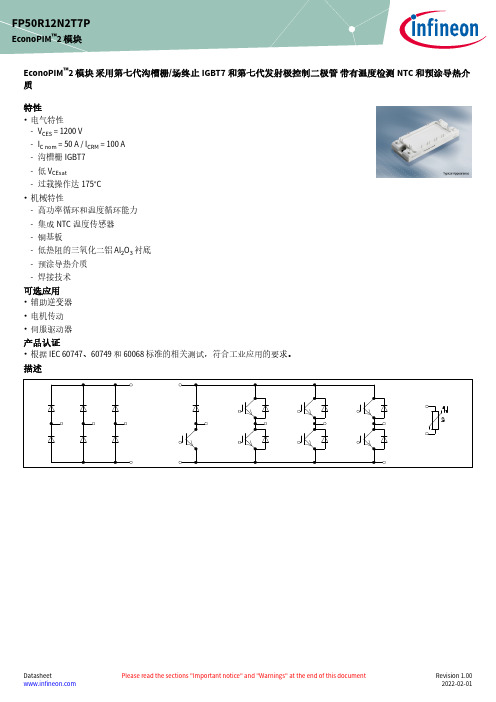
英飞凌 FP50R12N2T7P EconoPIM 2 模块 数据表
EconoPIM ™2 模块 采用第七代沟槽栅/场终止IGBT7和第七代发射极控制二极管 带有温度检测NTC 和预涂导热介质特性•电气特性-V CES = 1200 V-I C nom = 50 A / I CRM = 100 A -沟槽栅IGBT7-低 V CEsat-过载操作达175°C•机械特性-高功率循环和温度循环能力-集成NTC 温度传感器-铜基板-低热阻的三氧化二铝 Al 2O 3 衬底-预涂导热介质-焊接技术可选应用•辅助逆变器•电机传动•伺服驱动器产品认证•根据 IEC 60747、60749 和 60068标准的相关测试,符合工业应用的要求。
描述FP50R12N2T7PEconoPIM ™2 模块内容描述 . . . . . . . . . . . . . . . . . . . . . . . . . . . . . . . . . . . . . . . . . . . . . . . . . . . . . . . . . . . . . . . . . . . . . . . . . . . . . . . . . . . . . . . . .1特性 . . . . . . . . . . . . . . . . . . . . . . . . . . . . . . . . . . . . . . . . . . . . . . . . . . . . . . . . . . . . . . . . . . . . . . . . . . . . . . . . . . . . . . . . .1可选应用 . . . . . . . . . . . . . . . . . . . . . . . . . . . . . . . . . . . . . . . . . . . . . . . . . . . . . . . . . . . . . . . . . . . . . . . . . . . . . . . . . . . .1产品认证 . . . . . . . . . . . . . . . . . . . . . . . . . . . . . . . . . . . . . . . . . . . . . . . . . . . . . . . . . . . . . . . . . . . . . . . . . . . . . . . . . . . .1内容 . . . . . . . . . . . . . . . . . . . . . . . . . . . . . . . . . . . . . . . . . . . . . . . . . . . . . . . . . . . . . . . . . . . . . . . . . . . . . . . . . . . . . . . . .2 1封装 . . . . . . . . . . . . . . . . . . . . . . . . . . . . . . . . . . . . . . . . . . . . . . . . . . . . . . . . . . . . . . . . . . . . . . . . . . . . . . . . . . . . . . . . .3 2IGBT, 逆变器 . . . . . . . . . . . . . . . . . . . . . . . . . . . . . . . . . . . . . . . . . . . . . . . . . . . . . . . . . . . . . . . . . . . . . . . . . . . . . . . . .3 3二极管,逆变器 . . . . . . . . . . . . . . . . . . . . . . . . . . . . . . . . . . . . . . . . . . . . . . . . . . . . . . . . . . . . . . . . . . . . . . . . . . . . . . .5 4二极管,整流器 . . . . . . . . . . . . . . . . . . . . . . . . . . . . . . . . . . . . . . . . . . . . . . . . . . . . . . . . . . . . . . . . . . . . . . . . . . . . . . .6 5IGBT, 斩波器 . . . . . . . . . . . . . . . . . . . . . . . . . . . . . . . . . . . . . . . . . . . . . . . . . . . . . . . . . . . . . . . . . . . . . . . . . . . . . . . . .7 6Diode-斩波器 . . . . . . . . . . . . . . . . . . . . . . . . . . . . . . . . . . . . . . . . . . . . . . . . . . . . . . . . . . . . . . . . . . . . . . . . . . . . . . . .8 7负温度系数热敏电阻 . . . . . . . . . . . . . . . . . . . . . . . . . . . . . . . . . . . . . . . . . . . . . . . . . . . . . . . . . . . . . . . . . . . . . . . . .9 8特征参数图表 . . . . . . . . . . . . . . . . . . . . . . . . . . . . . . . . . . . . . . . . . . . . . . . . . . . . . . . . . . . . . . . . . . . . . . . . . . . . . . .10 9电路拓扑图 . . . . . . . . . . . . . . . . . . . . . . . . . . . . . . . . . . . . . . . . . . . . . . . . . . . . . . . . . . . . . . . . . . . . . . . . . . . . . . . . .16 10封装尺寸 . . . . . . . . . . . . . . . . . . . . . . . . . . . . . . . . . . . . . . . . . . . . . . . . . . . . . . . . . . . . . . . . . . . . . . . . . . . . . . . . . . .16 11模块标签代码 . . . . . . . . . . . . . . . . . . . . . . . . . . . . . . . . . . . . . . . . . . . . . . . . . . . . . . . . . . . . . . . . . . . . . . . . . . . . . . .17修订历史 . . . . . . . . . . . . . . . . . . . . . . . . . . . . . . . . . . . . . . . . . . . . . . . . . . . . . . . . . . . . . . . . . . . . . . . . . . . . . . . . . . .18免责声明 . . . . . . . . . . . . . . . . . . . . . . . . . . . . . . . . . . . . . . . . . . . . . . . . . . . . . . . . . . . . . . . . . . . . . . . . . . . . . . . . . . .191封装表 1绝缘参数特征参数代号标注或测试条件数值单位绝缘测试电压V ISOL RMS, f = 50 Hz, t = 1 min 2.5kV 模块基板材料Cu内部绝缘基本绝缘 (class 1, IEC 61140)Al2O3爬电距离d Creep端子至散热器10.0mm 电气间隙d Clear端子至散热器7.5mm 相对电痕指数CTI>200相对温度指数 (电)RTI封装140°C 表 2特征值特征参数代号标注或测试条件数值单位最小值典型值最大值杂散电感,模块L sCE35nH 模块引线电阻,端子-芯片R AA'+CC'T H=25°C, 每个开关 5.5mΩ模块引线电阻,端子-芯片R CC'+EE'T H=25°C, 每个开关 4.8mΩ储存温度T stg-40125°C 最高基板工作温度T BPmax150°CM5, 螺丝36Nm 模块安装的安装扭距M根据相应的应用手册进行安装重量G180g注:The current under continuous operation is limited to 50 A rms per connector pin.Storage and shipment of modules with TIM => see AN2012-072IGBT, 逆变器表 3最大标定值特征参数代号标注或测试条件数值单位集电极-发射极电压V CES T vj = 25 °C1200V 连续集电极直流电流I CDC T vj max = 175 °C T H = 90 °C50A 集电极重复峰值电流I CRM t P = 1 ms100A 栅极-发射极峰值电压V GES±20V表 4特征值特征参数代号标注或测试条件数值单位最小值典型值最大值集电极-发射极饱和电压V CE sat I C = 50 A, V GE = 15 V T vj = 25 °C 1.50 1.80VT vj = 125 °C 1.64T vj = 175 °C 1.72栅极阈值电压V GEth I C = 2 mA, V CE = V GE, T vj = 25 °C 5.15 5.80 6.45V 栅极电荷Q G V GE = ±15 V, V CE = 600 V0.92µC 内部栅极电阻R Gint T vj = 25 °C0Ω输入电容C ies f = 100 kHz, T vj = 25 °C, V CE = 25 V, V GE = 0 V11.1nF 反向传输电容C res f = 100 kHz, T vj = 25 °C, V CE = 25 V, V GE = 0 V0.039nF 集电极-发射极截止电流I CES V CE = 1200 V, V GE = 0 V T vj = 25 °C0.01mA 栅极-发射极漏电流I GES V CE = 0 V, V GE = 20 V, T vj = 25 °C100nA开通延迟时间(感性负载)t don I C = 50 A, V CE = 600 V,V GE = ±15 V, R Gon = 7.5 ΩT vj = 25 °C0.059µs T vj = 125 °C0.061T vj = 175 °C0.062上升时间(感性负载)t r I C = 50 A, V CE = 600 V,V GE = ±15 V, R Gon = 7.5 ΩT vj = 25 °C0.043µs T vj = 125 °C0.047T vj = 175 °C0.049关断延迟时间(感性负载)t doff I C = 50 A, V CE = 600 V,V GE = ±15 V, R Goff = 7.5 ΩT vj = 25 °C0.290µs T vj = 125 °C0.380T vj = 175 °C0.420下降时间(感性负载)t f I C = 50 A, V CE = 600 V,V GE = ±15 V, R Goff = 7.5 ΩT vj = 25 °C0.110µs T vj = 125 °C0.200T vj = 175 °C0.270开通损耗能量 (每脉冲)E on I C = 50 A, V CE = 600 V,Lσ = 35 nH, V GE = ±15 V,R Gon = 7.5 Ω, di/dt = 900A/µs (T vj = 175 °C)T vj = 25 °C 5.07mJ T vj = 125 °C 6.76T vj = 175 °C7.72关断损耗能量 (每脉冲)E off I C = 50 A, V CE = 600 V,Lσ = 35 nH, V GE = ±15 V,R Goff = 7.5 Ω, dv/dt =2900 V/µs (T vj = 175 °C)T vj = 25 °C 3.37mJ T vj = 125 °C 5.31T vj = 175 °C 6.58(待续)表 4(续) 特征值特征参数代号标注或测试条件数值单位最小值典型值最大值短路数据I SC V GE≤ 15 V, V CC = 800 V,V CEmax=V CES-L sCE*di/dt t P≤ 8 µs,T vj=150 °C190At P≤ 7 µs,T vj=175 °C180结-散热器热阻R thJH每个 IGBT, Valid with IFX pre-appliedThermal Interface Material0.777K/W 允许开关的温度范围T vj op-40175°C注:T vj op > 150°C is allowed for operation at overload conditions. For detailed specifications, please refer to AN 2018-14.3二极管,逆变器表 5最大标定值特征参数代号标注或测试条件数值单位反向重复峰值电压V RRM T vj = 25 °C1200V 连续正向直流电流I F50A 正向重复峰值电流I FRM t P = 1 ms100A I2t-值I2t V R = 0 V, t P = 10 ms T vj = 125 °C465A²sT vj = 175 °C420表 6特征值特征参数代号标注或测试条件数值单位最小值典型值最大值正向电压V F I F = 50 A, V GE = 0 V T vj = 25 °C 1.72 2.10VT vj = 125 °C 1.59T vj = 175 °C 1.52反向恢复峰值电流I RM I F = 35 A, V R = 600 V,V GE = -15 V, -di F/dt = 900A/µs (T vj = 175 °C)T vj = 25 °C31A T vj = 125 °C39T vj = 175 °C45恢复电荷Q r I F = 50 A, V R = 600 V,V GE = -15 V, -di F/dt = 900A/µs (T vj = 175 °C)T vj = 25 °C 3.96µC T vj = 125 °C7.37T vj = 175 °C9.89(待续)表 6(续) 特征值特征参数代号标注或测试条件数值单位最小值典型值最大值反向恢复损耗(每脉冲)E rec I F = 50 A, V R = 600 V,V GE = -15 V, -di F/dt = 900A/µs (T vj = 175 °C)T vj = 25 °C 1.31mJ T vj = 125 °C 2.52T vj = 175 °C 3.46结-散热器热阻R thJH每个二极管, Valid with IFX pre-appliedThermal Interface Material1.13K/W 允许开关的温度范围T vj op-40175°C注:T vj op > 150°C is allowed for operation at overload conditions. For detailed specifications, please refer to AN 2018-14.4二极管,整流器表 7最大标定值特征参数代号标注或测试条件数值单位反向重复峰值电压V RRM T vj = 25 °C1600V 最大正向均方根电流(每芯片)I FRMSM T H = 60 °C70A最大整流器输出均方根电流I RMSM T H = 60 °C100A 正向浪涌电流I FSM t P = 10 ms T vj = 25 °C560AT vj = 150 °C435I2t-值I2t t P = 10 ms T vj = 25 °C1570A²sT vj = 150 °C945表 8特征值特征参数代号标注或测试条件数值单位最小值典型值最大值正向电压V F I F = 50 A T vj = 150 °C 1.05V 反向电流I r T vj = 150 °C, V R = 1600 V1mA 结-散热器热阻R thJH每个二极管, Valid with IFX pre-appliedThermal Interface Material1.10K/W 允许开关的温度范围T vj, op-40150°C5IGBT, 斩波器表 9最大标定值特征参数代号标注或测试条件数值单位集电极-发射极电压V CES T vj = 25 °C1200V 连续集电极直流电流I CDC T vj max = 175 °C T H = 110 °C25A 集电极重复峰值电流I CRM t P = 1 ms50A 栅极-发射极峰值电压V GES±20V表 10特征值特征参数代号标注或测试条件数值单位最小值典型值最大值集电极-发射极饱和电压V CE sat I C = 25 A, V GE = 15 V T vj = 25 °C 1.60 1.85VT vj = 125 °C 1.74T vj = 175 °C 1.82栅极阈值电压V GEth I C = 0.525 mA, V CE = V GE, T vj = 25 °C 5.15 5.80 6.45V 栅极电荷Q G V GE = ±15 V, V CE = 600 V0.395µC 内部栅极电阻R Gint T vj = 25 °C0Ω输入电容C ies f = 100 kHz, T vj = 25 °C, V CE = 25 V, V GE = 0 V 4.77nF 反向传输电容C res f = 100 kHz, T vj = 25 °C, V CE = 25 V, V GE = 0 V0.017nF 集电极-发射极截止电流I CES V CE = 1200 V, V GE = 0 V T vj = 25 °C0.004mA 栅极-发射极漏电流I GES V CE = 0 V, V GE = 20 V, T vj = 25 °C100nA开通延迟时间(感性负载)t don I C = 25 A, V CE = 600 V,V GE = ±15 V, R Gon = 9.1 ΩT vj = 25 °C0.041µs T vj = 125 °C0.043T vj = 175 °C0.044上升时间(感性负载)t r I C = 25 A, V CE = 600 V,V GE = ±15 V, R Gon = 9.1 ΩT vj = 25 °C0.025µs T vj = 125 °C0.028T vj = 175 °C0.030关断延迟时间(感性负载)t doff I C = 25 A, V CE = 600 V,V GE = ±15 V, R Goff = 9.1 ΩT vj = 25 °C0.230µs T vj = 125 °C0.320T vj = 175 °C0.350下降时间(感性负载)t f I C = 25 A, V CE = 600 V,V GE = ±15 V, R Goff = 9.1 ΩT vj = 25 °C0.140µs T vj = 125 °C0.220T vj = 175 °C0.280(待续)表 10(续) 特征值特征参数代号标注或测试条件数值单位最小值典型值最大值开通损耗能量 (每脉冲)E on I C = 25 A, V CE = 600 V,Lσ = 35 nH, V GE = ±15 V,R Gon = 9.1 Ω, di/dt = 810A/µs (T vj = 175 °C)T vj = 25 °C 1.47mJ T vj = 125 °C 2.05T vj = 175 °C 2.39关断损耗能量 (每脉冲)E off I C = 25 A, V CE = 600 V,Lσ = 35 nH, V GE = ±15 V,R Goff = 9.1 Ω, dv/dt =3120 V/µs (T vj = 175 °C)T vj = 25 °C 1.65mJ T vj = 125 °C 2.58T vj = 175 °C 3.13短路数据I SC V GE≤ 15 V, V CC = 800 V,V CEmax=V CES-L sCE*di/dt t P≤ 8 µs,T vj=150 °C90At P≤ 7 µs,T vj=175 °C85结-散热器热阻R thJH每个 IGBT, Valid with IFX pre-appliedThermal Interface Material1.19K/W 允许开关的温度范围T vj op-40175°C注:T vj op > 150°C is allowed for operation at overload conditions. For detailed specifications, please refer to AN 2018-14.6Diode-斩波器表 11最大标定值特征参数代号标注或测试条件数值单位反向重复峰值电压V RRM T vj = 25 °C1200V 连续正向直流电流I F25A 正向重复峰值电流I FRM t P = 1 ms50A I2t-值I2t V R = 0 V, t P = 10 ms T vj = 125 °C125A²sT vj = 175 °C95表 12特征值特征参数代号标注或测试条件数值单位最小值典型值最大值正向电压V F I F = 25 A, V GE = 0 V T vj = 25 °C 1.83 2.30VT vj = 125 °C 1.70T vj = 175 °C 1.63(待续)表 12(续) 特征值特征参数代号标注或测试条件数值单位最小值典型值最大值反向恢复峰值电流I RM I F = 25 A, V R = 600 V,V GE = -15 V, -di F/dt = 810A/µs (T vj = 175 °C)T vj = 25 °C21.7A T vj = 125 °C26.7T vj = 175 °C29.8恢复电荷Q r I F = 25 A, V R = 600 V,V GE = -15 V, -di F/dt = 810A/µs (T vj = 175 °C)T vj = 25 °C 1.69µC T vj = 125 °C 3.29T vj = 175 °C 4.29反向恢复损耗(每脉冲)E rec I F = 25 A, V R = 600 V,V GE = -15 V, -di F/dt = 810A/µs (T vj = 175 °C)T vj = 25 °C0.63mJ T vj = 125 °C 1.28T vj = 175 °C 1.69结-散热器热阻R thJH每个二极管, Valid with IFX pre-appliedThermal Interface Material1.63K/W 允许开关的温度范围T vj op-40175°C注:T vj op > 150°C is allowed for operation at overload conditions. For detailed specifications, please refer to AN 2018-14.7负温度系数热敏电阻表 13特征值特征参数代号标注或测试条件数值单位最小值典型值最大值额定电阻值R25T NTC = 25 °C5kΩR100偏差ΔR/R T NTC = 100 °C, R100 = 493 Ω-55%耗散功率P25T NTC = 25 °C20mW B-值B25/50R2 = R25 exp[B25/50(1/T2-1/(298,15 K))]3375K B-值B25/80R2 = R25 exp[B25/80(1/T2-1/(298,15 K))]3411K B-值B25/100R2 = R25 exp[B25/100(1/T2-1/(298,15 K))]3433K 注:根据应用手册标定7 负温度系数热敏电阻9电路拓扑图图 110封装尺寸图 211模块标签代码图 3修订历史修订历史修订版本发布日期变更说明1.002022-02-01Initial version商标所有参照产品或服务名称和商标均为其各自所有者的财产。
Microchip HV98101 230VAC 离线式 LED 驱动器 评估板 用户指南说明书

HV98101 230V AC离线式LED驱动器评估板用户指南2017 Microchip Technology Inc.DS50002544A_CN请注意以下有关Microchip器件代码保护功能的要点:•Microchip的产品均达到Microchip数据手册中所述的技术指标。
•Microchip确信:在正常使用的情况下,Microchip系列产品是当今市场上同类产品中最安全的产品之一。
•目前,仍存在着恶意、甚至是非法破坏代码保护功能的行为。
就我们所知,所有这些行为都不是以Microchip数据手册中规定的操作规范来使用Microchip产品的。
这样做的人极可能侵犯了知识产权。
•Microchip愿与那些注重代码完整性的客户合作。
•Microchip或任何其他半导体厂商均无法保证其代码的安全性。
代码保护并不意味着我们保证产品是“牢不可破”的。
代码保护功能处于持续发展中。
Microchip承诺将不断改进产品的代码保护功能。
任何试图破坏Microchip代码保护功能的行为均可视为违反了《数字器件千年版权法案(Digital Millennium Copyright Act)》。
如果这种行为导致他人在未经授权的情况下,能访问您的软件或其他受版权保护的成果,您有权依据该法案提起诉讼,从而制止这种行为。
2017 Microchip Technology Inc.DS50002544A_CN 第3页EU Declaration of ConformityThis declaration of conformity is issued by the manufacturer.The development/evaluation tool is designed to be used for research and development in a laboratory environment. Thisdevelopment/evaluation tool is not a Finished Appliance, nor is it intended for incorporation into Finished Appliances that are made commercially available as single functional units to end users under EU EMC Directive 2004/108/EC and as supported by the European Commission's Guide for the EMC Directive 2004/108/EC (8th February 2010). This development/evaluation tool complies with EU RoHS2 Directive 2011/65/EU.This development/evaluation tool, when incorporating wireless and radio-telecom functionality, is in compliance with the essential requirement and other relevant provisions of the R&TTE Directive 1999/5/EC and the FCC rules as stated in the declaration of conformity provided in the module datasheet and the module product page available at . For information regarding the exclusive, limited warranties applicable to Microchip products, please see Microchip’s standard terms and conditions of sale, which are printed on our sales documentation and available at .Signed for and on behalf of Microchip Technology Inc. at Chandler, Arizona, USA.申明对象:HV98101 230V AC 离线式LED 驱动器评估板HV98101 230V AC 离线式LED驱动器评估板用户指南注:DS50002544A_CN第4页 2017 Microchip Technology Inc.HV98101 230V AC 离线式LED驱动器评估板用户指南2017 Microchip Technology Inc.DS50002544A_CN 第5页目录前言 (7)简介.......................................................................................................................7文档编排................................................................................................................7本指南使用约定.....................................................................................................8推荐读物................................................................................................................9Microchip 网站.......................................................................................................9客户支持................................................................................................................9文档版本历史 (9)第1章 产品概述1.1 简介...............................................................................................................111.2 HV98101器件概述. (11)1.2.1 HV98101器件主要特性 (11)1.3 HV98101 230V AC 离线式LED 驱动器评估板 (12)1.3.1 评估板技术规范 (12)1.4 HV98101 230V AC 离线式LED 驱动器评估板用户指南的内容 (12)第2章 安装和操作2.1 入门 (13)2.1.1 操作所需的其他工具 (13)2.2 设置过程........................................................................................................132.3 HV98101 230V AC 离线式LED 驱动器评估板工作原理 (14)2.4 测试评估板....................................................................................................142.5 典型波形........................................................................................................152.6 典型测量.. (19)附录A 原理图和布线图A.1 简介...............................................................................................................23A.2 评估板——原理图.........................................................................................24A.3 评估板——顶层覆铜和焊盘...........................................................................25A.4 评估板——顶层覆铜、焊盘和丝印................................................................25A.5 评估板——顶层丝印和焊盘...........................................................................26A.6 评估板——底层覆铜和焊盘 (26)附录B 物料清单(BOM )全球销售及服务网点 (29)HV98101 230V AC离线式LED驱动器评估板用户指南注:DS50002544A_CN第6页 2017 Microchip Technology Inc.HV98101 230V AC 离线式LED驱动器评估板用户指南前言所有文档均会过时,本文档也不例外。
THC63LVD827 Datasheet

IOVCC
G7
Power Power Supply Pin for IO inputs circuitry.
LVDSVCC
C5,D3
Power Power Supply Pins for LVDS Outputs.
PLLVCC
C7
Power Power Supply Pin for PLL circuitry.
The 2nd Link. LVDS OUT
The 2nd pixel output data when Dual out.
LVDS OUT LVDS Clock Out for 2nd Link.
IN
Pixel Data Inputs.
IN
Data Enable Input.
IN
Vsync Input.
1. Single in / Dual LVDS out
2. Single in / Single LVDS out
3. Double edge Single in / Dual LVDS out
• 2 LVDS data mapping to simplify PCB layout • Power down mode • Input clock triggering edge selectable by R/F pin • 6bit / 8bit modes selectable by 6B/8B pin
2/18
香港灏业科技 联系人:陈伟 手机:13510979382 QQ:744926516 地址:深圳市南山区高新南六道7B
THC63LVD827_Rev.1.00_E
Pin ription
Pin Name TA1+, TA1TB1+, TB1TC1+, TC1TD1+, TD1TCLK1+, TCLK1TA2+, TA2TB2+, TB2TC2+, TC2TD2+, TD2TCLK2+, TCLK2-
MCP23017 IO Expansion Board 用户手册说明书

产品概述我是一款基于I2C接口控制的I/O扩展模块,可外扩16Pin I/O口,支持同时使用多达8个,即可扩至128Pin I/O口,兼容3.3V和5V电平。
特点●I2C接口控制,仅需2根信号线,即可扩展出16个I/O口●I2C通信地址可设置,短接A0/A1/A2焊点可修改通信地址●提供PH2.0端子和焊盘两种接口类型,支持并联多个I2C模块●板载电平转换电路,可兼容3.3V/5V的工作电平●提供完善的配套资料手册(Raspberry/Micro:bit/Arduino/STM32示例程序和用户手册等)产品参数工作电压:5V/3.3V控制接口:I2C中断引脚:INTA、INTB扩展I/O口数量:16个产品尺寸:38mm × 23mm过孔直径: 2.0mm1接口定义I2C接口用于树莓派需要安装必要的WiringPi函数库,否则以下的示例程序可能无法正常工作。
安装方法详见:/wiki/Pioneer600_Datasheets在官网上找到对应产品,在产品资料打开下载路径,在wiki中下载示例程序:得到解压包,解压得到如下:将Raspberry Pi文件夹及其文件夹下的文件拷至树莓派。
2前置工作执行如下命令进行树莓派配置:sudo raspi-config选择Interfacing Options -> I2C -> yes 启动I2C内核驱动保存退出后,重启树莓派:sudo reboot重启后,运行命令查看,I2C,模块是否已启动:lsmod将会有如下的打印信息:如果显示i2c_bcm2835则表示I2C模块已启动。
将MCP23017模块按照上文接口定义连接至树莓派。
本示例程序已配置成将INTA与INTB内部连接在一起,INTA或INTB连接至0(Wiring PI) 均可测试通过。
34模块默认的I2C 地址为0X27,可通过焊点A2,A1,A0改变器件地址,默认情况下,A2,A1,A0 均未焊接,均为高电平,若将焊点短接,则连接至低电平。
- 1、下载文档前请自行甄别文档内容的完整性,平台不提供额外的编辑、内容补充、找答案等附加服务。
- 2、"仅部分预览"的文档,不可在线预览部分如存在完整性等问题,可反馈申请退款(可完整预览的文档不适用该条件!)。
- 3、如文档侵犯您的权益,请联系客服反馈,我们会尽快为您处理(人工客服工作时间:9:00-18:30)。
Figure 2. MIPI CSI-2 application diagram
2nd camera module with MIPI CSI-2 interface or parallel interface
If Parallel Output
MIPI CSI-2 1 x 800Mbps
Data (80Mbps -> 800Mbps)
■ Support for YUV, RGB and JPEG formats
■ Support for SMIA 8-10, 7-10, 6-10, 8-12, 7-12 & 6-12 DPCM/PCM decompression options
■ 1V8, 200MHz,12-bit parallel output interface
■ SMIA CCP2 receivers – Two camera interfaces support – 650Mbps class 2 receivers with selectable data/clock and data/strobe operation
■ Support for MIPI CSI-2 and SMIA CCP2 RAW6, RAW7, RAW8 (Generic), RAW10 and RAW12 Raw Bayer format data unpacking
Restricted Distribution
DRAFT Information classified Restricted Distribution - Do not copy (See last page for obligations)
STMIPID02
Dual mode MIPI CSI-2 / SMIA CCP2 de-serializer
Slave data lane module
Data lane control interface logic
Slave clock lane module
Clock lane control interface logic
Lane F T merging Low level protocol Byte to pixel conversion Decompression
STMIPID02 is fully configurable via an I2C compatible slave control I/F.
March 2009
Draft Rev 0.7
For further information contact your local STMicroelectronics sales office.
Draft Rev 0.7
Restricted Distribution
DRAFT Information classified Restricted Distribution - Do not copy (See last page for obligations)
STMIPID02
Block diagrams
STMIPID02’s 12-bit parallel output interface is capable of outputting de-serialized pixel data at rates up to 200MHz.
Pass through mode allows STMIPID02 to be used as a standalone MIPI D-PHY physical layer device.
Features
■ Dual mode camera de-serializer
■ MIPI CSI-2 receivers (Rev.0.9 compliant) – Two camera interfaces support – One 1.6Gbps dual data lane receiver for main camera with selectable 1/2 lane operation – One 800Mbps single data lane receiver for second camera – Each MIPI D-PHY interface with a 400MHz DDR clock lane – MIPI D-PHY Pass through mode
With this device an host with a standard 8-bit, 10bit or 12-bit parallel input interface can be connected to camera modules with either a MIPI CSI-2 or a SMIA CCP2 low voltage, fully differential bit-serial, low EMI interface.
MIPI CSI-2 RX Protocol
STMIPID02
OIF
SMIA CCP2 RX
Clock recovery & de-serializer
A
XSDN
1.2V voltage regulator (LDO)
Power on reset
JTAG controller
Clock manager
STMIPID02
DDR Clock (40MHz -> 400MHz)
Main camera module with MIPI CSI-2 interface
MIPI CSI-2 2 x 800Mbps
Data2 (80Mbps -> 800Mbps)
Data1 (80Mbps -> 800Mbps)
DATA2P1
DATA2N1
Doubles as CCP2 data & clock/strobe
inputs
Data Lane 1.1 80-800Mbps DATA1P1 DATA1N1
Clock Lane 1 40-400MHz
CLKP1 CLKN1
Slave data lane module
■ Integrated power-on-reset cell
■ Digital power supply: 1.7V to 1.9V
■ Integrated 1.2V regulator for D-PHY and core logic
■ VFBGA 49pin 3.0mm x 3.0mm x1.0mm F7x7 0.4mm pitch, 0.25mm ball package
■ MIPI CSI-2 short packet interrupt output
■ 2-wires 100/400 kHz control interface (I2C compatible slave) to configure D-PHY timeouts and pixel data unpacking/decompression options
■ HSYNC, VSYNC and continuous PCLK output data qualification signal
■ Tristate-able output for dual camera systems
■ Error interrupt output (D-PHY and protocol)
// pixel data
Baseband
or
application processor or
multi-media processor or
‘backend IC’
Draft Rev 0.7
3/52
STMIPID02
Main camera module with SMIA CCP2 interface
SMIA CCP2 Class 2 1 x 650Mbps
Data (up to 650Mbps)
Clock / Strobe 100/400 kHz I2C
6-b, 7-b, 8-b, 10-b or
An interrupt output for every MIPI CSI-2 short packet.
Power management is simplified by the presence of an integrated 1.2V regulator to supply the MIPI D-PHY receiver and core logic.
Figure 3. SMIA CCP2 application diagram
2nd camera module with SMIA CCP2 interface or Parallel Interface
If Parallel Output
SMIA CCP2 Class 2 1 x 650Mbps Data (up to 650Mbps) Clock / Strobe
STMIPID02
Figure 1. Block diagram
Doubles as CCP2 data & clock/strobe
inputs
Data Lane 2 80-800Mbps DATA1P2 DATA1N2
Clock Lane 2 40-400MHz
CLKP2 CLKN2
Data Lane 1.2 80-800Mbps
Data lane control interface logic
Slave clock lane module
Clock lane control interface logic
MIPI D-PHY RX
Slave data lane module