74LVTH16652MTDX中文资料
HD74ALVCH162260资料

2B H L 2B0 *1 2B0 *1 H L 2B0 *1 Z Z Active Active
H : High level L : Low level X : Immaterial Z : High impedance Note: 1. Output level before the indicated steady state input conditions were established.
3
元器件交易网
HD74ALVCH162260
Absolute Maximum Ratings
Item
Symbol
Ratings
Unit Conditions
Supply voltage
VCC
Input voltage *1, 2
VI
Output voltage *1, 2 Input clamp current Output clamp current Continuous output current VCC, GND current / pin Maximum power dissipation at Ta = 55°C (in still air) *3
HD74ALVCH162260
Logic Diagram
LE1B 2 LE2B 27
30
LEA1B LEA2B 55
OE2B 56 OE1B 29
OEA 1
28
SEL
8
A1
C1 G1
1
1D
1
C1
1D
C1
1D
C1 1D
To eleven other channels
23
1B1
6
2B1
74LVT162245MTDX中文资料

© 2005 Fairchild Semiconductor Corporation DS012446January 1999Revised June 200574LVT162245 • 74LVTH162245 Low Voltage 16-Bit Transceiver with 3-STATE Outputs and 25: Series Resistors in A Port Outputs74LVT162245 • 74LVTH162245Low Voltage 16-Bit Transceiver with 3-STATE Outputs and 25: Series Resistors in A Port OutputsGeneral DescriptionThe LVT162245 and LVTH162245 contains sixteen non-inverting bidirectional buffers with 3-STATE outputs and is intended for bus oriented applications. The device is byte controlled. Each byte has separate control inputs which can be shorted together for full 16-bit operation. The T/R inputs determine the direction of data flow through the device. The OE inputs disable both the A and B ports by placing them in a high impedance state.The LVT162245 and LVTH162245 are designed with equivalent 25: series resistance in both the HIGH and LOW states on the A Port outputs. This design reduces line noise in applications such as memory address drivers,clock drivers, and bus transceivers/transmitters.The LVTH162245 data inputs include bushold, eliminating the need for external pull-up resistors to hold unused inputs.These non-inverting transceivers are designed for low volt-age (3.3V) V CC applications, but with the capability to pro-vide a TTL interface to a 5V environment. The LVT162245and LVTH162245 are fabricated with an advanced BiCMOS technology to achieve high speed operation simi-lar to 5V ABT while maintaining a low power dissipation.Featuress Input and output interface capability to systems at 5V V CC s Bushold data inputs eliminate the need for external pull-up resistors to hold unused inputs (74LVTH162245),also available without bushold feature (74LVT162245).s Live insertion/extraction permitteds Power Up/Down high impedance provides glitch-free bus loading s A Port outputs include equivalent series resistance of 25: making external termination resistors unnecessary and reducing overshoot and undershoot s A Port outputs source/sink r 12 mA.B Port outputs source/sink 32 mA/ 64 mA s Functionally compatible with the 74 series 162245s Latch-up performance exceeds 500 mA s ESD performance:Human-body model ! 2000V Machine model ! 200V Charged-device model ! 1000Vs Also packaged in plastic Fine Pitch Ball Grid Array (FBGA)Ordering Code:Note 1: Ordering code “G” indicates Trays.Note 2: Devices also available in Tape and Reel. Specify by appending the suffix letter “X” to the ordering code.Order Number Package Number Package Description74LVT162245G (Note 1)(Note 2)BGA54A (Preliminary)54-Ball Fine-Pitch Ball Grid Array (FBGA), JEDEC MO-205, 5.5mm Wide 74LVT162245MEA (Note 2)MS48A 48-Lead Small Shrink Outline Package (SSOP), JEDEC MO-118, 0.300" Wide 74LVT162245MTD (Note 2)MTD4848-Lead Thin Shrink Small Outline Package (TSSOP), JEDEC MO-153, 6.1mm Wide 74LVTH162245G (Note 1)(Note 2)BGA54A 54-Ball Fine-Pitch Ball Grid Array (FBGA), JEDEC MO-205, 5.5mm Wide 74LVTH162245MEA MS48A 48-Lead Small Shrink Outline Package (SSOP), JEDEC MO-118, 0.300" Wide [TUBE]74LVTH162245MEX MS48A 48-Lead Small Shrink Outline Package (SSOP), JEDEC MO-118, 0.300" Wide [TAPE and REEL]74LVTH162245MTD MTD4848-Lead Thin Shrink Small Outline Package (TSSOP), JEDEC MO-153, 6.1mm Wide [TUBE]74LVTH162245MTXMTD4848-Lead Thin Shrink Small Outline Package (TSSOP), JEDEC MO-153, 6.1mm Wide [TAPE and REEL] 274L V T 162245 • 74L V T H 162245Logic SymbolConnection DiagramsPin Assignments for SSOP and TSSOPPin Assignment for FBGA(Top Thru View)Pin DescriptionsFBGA Pin AssignmentsTruth TablesH HIGH Voltage LevelL LOW Voltage Level X ImmaterialZ High ImpedancePin Names DescriptionOE n Output Enable Input (Active LOW)T/R n Transmit/Receive Input A 0–A 15Side A Inputs/3-STATE Outputs B 0–B 15Side B Inputs/3-STATE Outputs NCNo Connect123456A B 0NC T/R 1OE 1NC A 0B B 2B 1NC NC A 1A 2C B 4B 3V CC V CC A 3A 4D B 6B 5GND GND A 5A 6E B 8B 7GND GND A 7A 8F B 10B 9GND GND A 9A 10G B 12B 11V CC V CC A 11A 12H B 14B 13NC NC A 13A 14JB 15NCT/R 2OE 2NCA 15Inputs OutputsOE 1T/R 1L L Bus B 0–B 7 Data to Bus A 0–A 7L H Bus A 0–A 7 Data to Bus B 0–B 7HXHIGH-Z State on A 0–A 7, B 0–B 7Inputs OutputsOE 2T/R 2L L Bus B 8–B 15 Data to Bus A 8–A 15L H Bus A 8–A 15 Data to Bus B 8–B 15HXHIGH-Z State on A 8–A 15, B 8–B 1574LVT162245 • 74LVTH162245Functional DescriptionThe LVT162245 and LVTH162245 contain sixteen non-inverting bidirectional buffers with 3-STATE outputs. The device is byte controlled with each byte functioning identi-cally, but independent of the other. The control pins can be shorted together to obtain full 16-bit operation.Logic DiagramsPlease note that these diagrams are provided only for the understanding of logic operations and should not be used to estimate propagation delays. 474L V T 162245 • 74L V T H 162245Absolute Maximum Ratings (Note 3)Recommended Operating ConditionsNote 3: Absolute Maximum continuous ratings are those values beyond which damage to the device may occur. Exposure to these conditions or conditions beyond those indicated may adversely affect device reliability. Functional operation under absolute maximum rated conditions is not implied. Note 4: I O Absolute Maximum Rating must be observed.DC Electrical CharacteristicsSymbol ParameterValueConditionsUnits V CC Supply Voltage 0.5 to 4.6V V I DC Input Voltage 0.5 to 7.0VV O Output Voltage 0.5 to 7.0Output in 3-STATEV 0.5 to 7.0Output in HIGH or LOW State (Note 4)I IK DC Input Diode Current 50V I GND mA I OK DC Output Diode Current 50V O GND mA I O DC Output Current64V O ! V CC Output at HIGH State mA 128V O ! V CCOutput at LOW StateI CC DC Supply Current per Supply Pin r 64mA I GND DC Ground Current per Ground Pin r 128mAT STGStorage Temperature65 to 150q CSymbol ParameterMin Max Units V CC Supply Voltage 2.7 3.6V V I Input Voltage5.5V I OH HIGH-Level Output Current B Port 32mA A Port 12I OL LOW-Level Output Current B Port 64mAA Port12T AFree Air Operating Temperature40 85q C 't/'VInput Edge Rate, V IN 0.8V –2.0V, V CC 3.0V10ns/VSymbol ParameterV CC T A 40q C to 85q C Units Conditions(V)MinMax V IK Input Clamp Diode Voltage 2.7 1.2V I I 18 mA V IH Input HIGH Voltage 2.7–3.6 2.0V V O d 0.1V or V IL Input LOW Voltage 2.7–3.60.8V V O t V CC 0.1V V OHOutput HIGH VoltageA Port 3.0 2.0V I OH 12 mA 2.7–3.6V CC 0.2V I OH 100 P A B Port2.7 2.4V I OH 8 mA3.0 2.0I OH 32 mA V OLOutput LOW VoltageA Port3.00.8V I OL 12 mA 2.70.2VI OL 100 P A B Port2.70.5VI OL 24 mA 3.00.4I OL 16 mA 3.00.5I OL 32 mA 3.00.55I OL 64 mA I I(HOLD)Bushold Input Minimum Drive3.075P A V I 0.8V (Note 5) 75V I 2.0V I I(OD)Bushold Input Over-Drive 3.0500P A (Note 6)(Note 5)Current to Change State 500(Note 7)I IInput Current3.610P AV I 5.5V Control Pins 3.6r 1V I 0V or V CC Data Pins3.6 5V I 0V 1V I V CCI OFFPower Off Leakage Current 0r 100P A 0V d V I or V O d 5.5V74LVT162245 • 74LVTH162245DC Electrical Characteristics (Continued)Note 5: Applies to Bushold versions only (74LVTH162245).Note 6: An external driver must source at least the specified current to switch from LOW-to-HIGH.Note 7: An external driver must sink at least the specified current to switch from HIGH-to-LOW.Note 8: This is the increase in supply current for each input that is at the specified voltage level rather than V CC or GND.Dynamic Switching Characteristics (Note 9)Note 9: Characterized in SSOP package. Guaranteed parameter, but not tested.Note 10: Max number of outputs defined as (n). n 1 data inputs are driven 0V to 3V. Output under test held LOW.Symbol ParameterV CC T A 40q C to 85q C Units Conditions(V)MinMax I PU/PD Power Up/Down 0–1.5V r 100P A V O 0.5V to 3.0V 3-STATE CurrentV I GND to V CC I OZL 3-STATE Output Leakage Current 3.6 5P A V O 0.5V I OZL 3-STATE Output Leakage Current 3.6 5P A V O 0.0V (Note 5)I OZH 3-STATE Output Leakage Current 3.65P A V O 3.0V I OZH 3-STATE Output Leakage Current3.65P A V O 3.6V (Note 5)I OZH 3-STATE Output Leakage Current 3.610P A V CC V O d 5.5V I CCH Power Supply Current 3.60.19mA Outputs HIGH I CCL Power Supply Current 3.65mA Outputs LOW I CCZ Power Supply Current 3.60.19mA Outputs Disabled I CCZ Power Supply Current3.60.19mA V CC d V O d 5.5V,Outputs Disabled 'I CCIncrease in Power Supply Current 3.60.2mAOne Input at V CC 0.6V (Note 8)Other Inputs at V CC or GNDSymbol ParameterV CC T A 25q C Units Conditions (V)MinTyp MaxC L 50 pF, R L 500:V OLP Quiet Output Maximum Dynamic V OL 3.30.8V (Note 10)V OLVQuiet Output Minimum Dynamic V OL3.30.8V(Note 10) 674L V T 162245 • 74L V T H 162245AC Electrical CharacteristicsNote 11: Skew is defined as the absolute value of the difference between the actual propagation delay for any two separate outputs of the same device. The specification applies to any outputs switching in the same direction, either HIGH-to-LOW (t OSHL ) or LOW-to-HIGH (t OSLH ).Capacitance (Note 12)Note 12: Capacitance is measured at frequency f 1 MHz, per MIL-STD-883, Method 3012.SymbolParameterT A 40q C to 85q CUnitsC L 50 pF, R L 500:V CC 3.3V r 0.3V V CC 2.7V MinMax MinMax t PLH Propagation Delay Data to A Port Output1.0 4.0 1.0 4.6ns t PHL 1.0 3.7 1.0 4.1t PLH Propagation Delay Data to B Port Output 1.0 3.5 1.0 3.9ns t PHL 1.0 3.5 1.0 3.9t PZH Output Enable Time for A Port Output 1.0 5.3 1.0 6.3ns t PZL 1.0 5.6 1.07.2t PZH Output Enable Time for B Port Output 1.0 4.6 1.0 5.4ns t PZL 1.0 5.3 1.0 6.9t PHZ Output Disable Time for A Port Output 1.5 5.6 1.5 6.3ns t PLZ 1.5 5.5 1.5 5.5t PHZ Output Disable Time for B Port Output 1.5 5.4 1.5 6.1ns t PLZ 1.55.1 1.55.4t OSHL A Port Output to Output Skew 1.0 1.0ns t OSLH (Note 11)t OSHL B Port Output to Output Skew 1.01.0ns t OSLH(Note 11)Symbol ParameterConditionsTypical Units C IN Input Capacitance V CC 0V, V I 0V or V CC 4pF C I/OInput/Output CapacitanceV CC 3.0V, V O 0V or V CC8pF74LVT162245 • 74LVTH162245Physical Dimensionsinches (millimeters) unless otherwise noted54-Ball Fine-Pitch Ball Grid Array (FBGA), JEDEC MO-205, 5.5mm WidePackage Number BGA54A 874L V T 162245 • 74L V T H 162245Physical Dimensions inches (millimeters) unless otherwise noted (Continued)48-Lead Small Shrink Outline Package (SSOP), JEDEC MO-118, 0.300" WidePackage Number MS48A974LVT162245 • 74LVTH162245 Low Voltage 16-Bit Transceiver with 3-STATE Outputs and 25: Series Resistors in A Port OutputsPhysical Dimensions inches (millimeters) unless otherwise noted (Continued)48-Lead Thin Shrink Small Outline Package (TSSOP), JEDEC MO-153, 6.1mm WidePackage Number MTD48Fairchild does not assume any responsibility for use of any circuitry described, no circuit patent licenses are implied and Fairchild reserves the right at any time without notice to change said circuitry and specifications.LIFE SUPPORT POLICYFAIRCHILD ’S PRODUCTS ARE NOT AUTHORIZED FOR USE AS CRITICAL COMPONENTS IN LIFE SUPPORT DEVICES OR SYSTEMS WITHOUT THE EXPRESS WRITTEN APPROVAL OF THE PRESIDENT OF FAIRCHILD SEMICONDUCTOR CORPORATION. As used herein:1.Life support devices or systems are devices or systems which, (a) are intended for surgical implant into the body, or (b) support or sustain life, and (c) whose failure to perform when properly used in accordance with instructions for use provided in the labeling, can be rea-sonably expected to result in a significant injury to the user.2. A critical component in any component of a life support device or system whose failure to perform can be rea-sonably expected to cause the failure of the life support device or system, or to affect its safety or effectiveness.。
TC74LVX02F_07中文资料

TOSHIBA CMOS Digital Integrated Circuit Silicon Monolithic TC74LVX02F,TC74LVX02FN,TC74LVX02FT Quad 2-Input NOR GateThe TC74LVX02F/ FN/ FT is a high-speed CMOS 2-input NORgate fabricated with silicon gate CMOS technology. Designed for use in 3-V systems, it achieves high-speed operation while maintaining the CMOS low power dissipation.This device is suitable for low-voltage and battery operated systems.The internal circuit is composed of 3 stages including buffer output, which provide high noise immunity and stable output. An input protection circuit ensures that 0 to 5.5V can be applied to the input pins without regard to the supply voltage. This device can be used to interface 5V to 3V systems and two supply systems such as battery back up. This circuit prevents device destruction due to mismatched supply and input voltages. Features•High-speed: t pd= 4.5 ns (typ.) (V CC= 3.3 V)•Low-power dissipation: I CC= 2 μA (max) (Ta = 25°C) •Input voltage level: V IL= 0.8 V (max) (V CC= 3 V)V IH= 2.0 V (min) (V CC= 3 V)•Power-down protection provided on all inputs •Balanced propagation delays: t pLH∼ − t pHL•Low noise: V OLP= 0.5 V (max)•Pin and function compatible with 74HC02 Note: xxxFN (JEDEC SOP) is not available in Japan.TC74LVX02FTC74LVX02FNTC74LVX02FTWeightSOP14-P-300-1.27A : 0.18 g (typ.) SOL14-P-150-1.27 : 0.12 g (typ.) TSSOP14-P-0044-0.65A : 0.06 g (typ.)Pin Assignment (top view)IEC Logic SymbolTruth TableInputs Outputs A BYL L H L H L H L L H HLAbsolute Maximum Ratings (Note)Characteristics Symbol Rating UnitSupply voltage range V CC −0.5 to 7.0 V DC input voltage V IN −0.5 to 7.0 V DC output voltage V OUT −0.5 to V CC + 0.5VInput diode current I IK −20 mA Output diode current I OK ±20 mA DC output current I OUT ±25 mA DC V CC /ground current I CC ±50 mA Power dissipation P D 180 mW Storage temperatureT stg−65 to 150°CNote: Exceeding any of the absolute maximum ratings, even briefly, lead to deterioration in IC performance or even destruction.Using continuously under heavy loads (e.g. the application of high temperature/current/voltage and thesignificant change in temperature, etc.) may cause this product to decrease in the reliability significantly even if the operating conditions (i.e. operating temperature/current/voltage, etc.) are within the absolute maximum ratings and the operating ranges.Please design the appropriate reliability upon reviewing the Toshiba Semiconductor Reliability Handbook (“Handling Precautions”/“Derating Concept and Methods”) and individual reliability data (i.e. reliability test report and estimated failure rate, etc).V CC 14 4B 4A 4Y 3B 3A13 12 11 10 9 81A 12345671B 2Y 2A 2B 1Y GND3Y (3)(2)(6)(5)(9)(8)(12)(11)1B 1A 2B 2A 3B 3A 4B4A (1) (4) (10) (13)1Y 2Y 3Y 4Y> 1Operating Ranges (Note)Characteristics Symbol Rating UnitSupply voltage V CC 2.0 to 3.6 V Input voltage V IN 0 to 5.5 V Output voltage V OUT 0 to V CC V Operating temperature T opr −40 to 85 °C Input rise and fall timedt/dv0 to 100ns/VNote: The operating ranges must be maintained to ensure the normal operation of the device. Unused inputs must be tied to either VCC or GND.Electrical CharacteristicsDC CharacteristicsTa = 25°CTa = −40 to85°CCharacteristics Symbol Test ConditionV CC (V)MinTyp.Max Min Max Unit2.0 1.5 ⎯⎯ 1.5 ⎯ 3.0 2.0 ⎯ ⎯ 2.0 ⎯ H-levelV IH⎯3.6 2.4 ⎯ ⎯ 2.4 ⎯2.0 ⎯ ⎯ 0.5 ⎯ 0.53.0 ⎯ ⎯ 0.8 ⎯ 0.8 Input voltageL-level V IL⎯3.6⎯⎯ 0.8 ⎯ 0.8VI OH = −50 μA2.0 1.9 2.0 ⎯ 1.9 ⎯ I OH = −50 μA3.0 2.9 3.0 ⎯ 2.9 ⎯ H-levelV OHV IN = V IL I OH = −4 mA3.02.58⎯⎯ 2.48 ⎯I OL = 50 μA 2.0 ⎯ 0 0.1 ⎯ 0.1I OL = 50 μA 3.0 ⎯ 0 0.1 ⎯ 0.1Output voltageL-level V OLV IN = V IHor V ILI OL = 4 mA 3.0 ⎯ ⎯ 0.36 ⎯ 0.44VInput leakage current I IN V IN = 5.5 V or GND 3.6 ⎯ ⎯±0.1⎯±1.0μA Quiescent supply currentI CCV IN = V CC or GND3.6⎯⎯ 2.0 ⎯ 20.0μAAC Characteristics (input: t r = t f = 3 ns)Ta = 25°C Ta = −40 to85°CCharacteristics Symbol Test ConditionV CC (V)C L (pF)Min Typ.Max Min MaxUnit15 ⎯ 5.9 10.7 1.0 13.5t pLH2.750 ⎯ 8.4 14.2 1.0 17.015 ⎯ 4.5 6.6 1.0 8.0 Propagation delay timet pHL ⎯3.3 ± 0.350⎯7.0 10.1 1.0 11.5ns2.7 50 ⎯ ⎯ 1.5 ⎯ 1.5 Output to output skew t osLH t osHL (Note 1)3.3 ± 0.350 ⎯ ⎯1.5⎯1.5ns Input capacitanceC IN (Note 2)⎯ 4 10 ⎯10 pF Power dissipation capacitanceC PD(Note 3)⎯15⎯⎯⎯pFNote 1: Parameter guaranteed by design.(t osLH = |t pLHm − t pLHn |, t osHL = |t pHLm − t pHLn |) Note 2: Parameter guaranteed by design.Note 3: C PD is defined as the value of the internal equivalent capacitance which is calculated from the operatingcurrent consumption.Average operating current can be obtained by the equation: I CC (opr) = C PD ・V CC ・f IN + I CC /4 (per gate)Noise Characteristics (Ta = 25°C, input: t r = t f = 3 ns, C L = 50 pF)Characteristics SymbolTest ConditionV CC (V)Typ.LimitUnitQuiet output maximum dynamic V OL V OLP ⎯ 3.3 0.3 0.5 V Quiet output minimum dynamic V OL V OLV ⎯ 3.3 −0.3 −0.5V Minimum high level dynamic input voltage V IHV IHD ⎯ 3.3 ⎯ 2.0 V Maximum low level dynamic input voltage V ILV ILD⎯ 3.3 ⎯ 0.8 VInput Equivalent CircuitPackage DimensionsWeight: 0.18 g (typ.)Package Dimensions (Note)Note: This package is not available in Japan. Weight: 0.12 g (typ.)Package DimensionsWeight: 0.06 g (typ.)RESTRICTIONS ON PRODUCT USE20070701-EN GENERAL •The information contained herein is subject to change without notice.•TOSHIBA is continually working to improve the quality and reliability of its products. Nevertheless, semiconductor devices in general can malfunction or fail due to their inherent electrical sensitivity and vulnerability to physical stress. It is the responsibility of the buyer, when utilizing TOSHIBA products, to comply with the standards of safety in making a safe design for the entire system, and to avoid situations in which a malfunction or failure of such TOSHIBA products could cause loss of human life, bodily injury or damage to property.In developing your designs, please ensure that TOSHIBA products are used within specified operating ranges as set forth in the most recent TOSHIBA products specifications. Also, please keep in mind the precautions and conditions set forth in the “Handling Guide for Semiconductor Devices,” or “TOSHIBA Semiconductor Reliability Handbook” etc.• The TOSHIBA products listed in this document are intended for usage in general electronics applications (computer, personal equipment, office equipment, measuring equipment, industrial robotics, domestic appliances, etc.).These TOSHIBA products are neither intended nor warranted for usage in equipment that requires extraordinarily high quality and/or reliability or a malfunction or failure of which may cause loss of human life or bodily injury (“Unintended Usage”). Unintended Usage include atomic energy control instruments, airplane or spaceship instruments, transportation instruments, traffic signal instruments, combustion control instruments, medical instruments, all types of safety devices, etc.. Unintended Usage of TOSHIBA products listed in his document shall be made at the customer’s own risk.•The products described in this document shall not be used or embedded to any downstream products of which manufacture, use and/or sale are prohibited under any applicable laws and regulations.• The information contained herein is presented only as a guide for the applications of our products. No responsibility is assumed by TOSHIBA for any infringements of patents or other rights of the third parties which may result from its use. No license is granted by implication or otherwise under any patents or other rights of TOSHIBA or the third parties.• Please contact your sales representative for product-by-product details in this document regarding RoHS compatibility. Please use these products in this document in compliance with all applicable laws and regulations that regulate the inclusion or use of controlled substances. Toshiba assumes no liability for damage or losses occurring as a result of noncompliance with applicable laws and regulations.。
SN74LVC16T245中文资料

元器件交易网元器件交易网IMPORTANT NOTICETexas Instruments Incorporated and its subsidiaries (TI) reserve the right to make corrections, modifications,enhancements, improvements, and other changes to its products and services at any time and to discontinueany product or service without notice. Customers should obtain the latest relevant information before placingorders and should verify that such information is current and complete. All products are sold subject to TI’s termsand conditions of sale supplied at the time of order acknowledgment.TI warrants performance of its hardware products to the specifications applicable at the time of sale inaccordance with TI’s standard warranty. T esting and other quality control techniques are used to the extent TIdeems necessary to support this warranty. Except where mandated by government requirements, testing of allparameters of each product is not necessarily performed.TI assumes no liability for applications assistance or customer product design. Customers are responsible fortheir products and applications using TI components. T o minimize the risks associated with customer productsand applications, customers should provide adequate design and operating safeguards.TI does not warrant or represent that any license, either express or implied, is granted under any TI patent right,copyright, mask work right, or other TI intellectual property right relating to any combination, machine, or processin which TI products or services are used. Information published by TI regarding third-party products or servicesdoes not constitute a license from TI to use such products or services or a warranty or endorsement thereof.Use of such information may require a license from a third party under the patents or other intellectual propertyof the third party, or a license from TI under the patents or other intellectual property of TI.Reproduction of information in TI data books or data sheets is permissible only if reproduction is withoutalteration and is accompanied by all associated warranties, conditions, limitations, and notices. Reproductionof this information with alteration is an unfair and deceptive business practice. TI is not responsible or liable forsuch altered documentation.Resale of TI products or services with statements different from or beyond the parameters stated by TI for thatproduct or service voids all express and any implied warranties for the associated TI product or service andis an unfair and deceptive business practice. TI is not responsible or liable for any such statements.Following are URLs where you can obtain information on other Texas Instruments products and applicationsolutions:Products ApplicationsAmplifiers Audio /audioData Converters Automotive /automotiveDSP Broadband /broadbandInterface Digital Control /digitalcontrolLogic Military /militaryPower Mgmt Optical Networking /opticalnetworkMicrocontrollers Security /securityTelephony /telephonyVideo & Imaging /videoWireless /wirelessMailing Address:Texas InstrumentsPost Office Box 655303 Dallas, Texas 75265Copyright 2005, Texas Instruments Incorporated。
74HC165中文资料
Vcc=最小,VIK=-12mA
Vcc = 最 小 VIH = 2V VIL= 0.8V, IOH = -800µA
‘165
最小
最大
-1.5
2.4
单位
V
V V
uA
mA MHz
ns ns ns ns ns ns ns
单位
V V
三毛电子世界
海纳电子资讯网:www.fpga-arm.com 为您提供各种IC中文资料
MHz ns ns ns ns ns
ns
[2]: fmax 最大时钟频率。tPLH输出由低电平到高电平传输延迟时间 tPHL输出由高电平到低 电平传输延迟时间
三毛电子世界
海纳电子资讯网:www.fpga-arm.com 为您提供各种IC中文资料
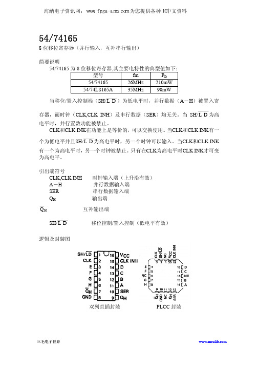
54/74165
8 位移位寄存器(并行输入,互补串行输出)
简要说明
54/74165 为 8 位移位寄存器,其主要电特性的典型值如下:
型号
fm
PD
54/74165
26MHz 210mW
54/74LS165A
35MHz
90mW
____
参
数[2]
fmax
tPLH tPHL
→ __ _
LD
__
QH, Q H
→ tPLH
CLK
__
QH, Q H
tPHL
→ tPLH H
QH
tPHL
tPLH tPHL
→ __
H QH
测试条件 Vcc =5V,CL=15Pf,RL=400Ω
‘165
最小 24
最大
31
40 24
31 17 36 27 27
74LVTH16244TTR, 规格书,Datasheet 资料

1/13February 2004sHIGH SPEED:t PD =3.2ns (MAX.)at T A =85°C V CC =3.0V sLOW POWER DISSIPATION HIGH LEVEL OUTPUT:I CC =190µA (MAX.)at T A =85°C sOUTPUT IMPEDANCE:|I OH |=32mA,I OL =64mA (MIN at V CC =3.0V)|I OH |=8mA,I OL =24mA (MIN at V CC =2.7V)sBALANCED PROPAGATION DELAYS:t PLH ≅t PHLsPOWER DOWN PROTECTION ON INPUTS AND OUTPUTSsCOMPATIBLE WITH TTL OUTPUTS:V IH =2V (MIN),V IL =0.8V(MAX)at V CC =2.7to 3.6VsPOWER-UP/DOWN 3-STATE:I OZPU =100µA MAX at V CC =0V to 1.5V,V CC =1.5V to 0V,T A =85°Cs BUS HOLD PROVIDED ON DATA INPUTS sOPERATING VOLTAGE RANGE:V CC (OPR)=2.7V to 3.6VsPIN AND FUNCTION COMPATIBLE WITH 74SERIES H16244sLATCH-UP PERFORMANCE EXCEEDS 500mA (JESD 17)DESCRIPTIONThe 74LVTH16244is a low voltage BiCMOS 16BIT BUS BUFFER (NON-INVERTED)fabricated with sub-micron silicon gate and five-layer metal wiring BiCMOS technology.It is ideal and full specified for hot-insertion and high speed 3.3V ap-plications;the power-up/down 3-state circuitry places the outputs in the high impedance state during power-up/down,which prevents driver con-flict.This function is guaranteed when V CC is be-tween 0and 1.5V.It can be interfaced to 3.3V sig-nal environment for both inputs and outputs.Any nG output control governs four BUS BUFFERS.Output Enable input (nG)tied together gives full 16-bit operation.When nG is LOW,the outputs are on.When nG is HIGH,the output are in high impedance state effectively isolated.Bus hold on data inputs is provided in order to eliminate the need for external pull-up or pull-down resistors.All inputs and outputs are equipped with protec-tion circuits against static discharge,giving them ESD immunity and transient excess voltage.74LVTH16244LOW VOLTAGE BICMOS 16BIT BUS BUFFER WITH BUS HOLD AND POWER UP 3-STATEORDER CODESPACKAGE T &RTSSOP4874LVTH16244TTR TFBGA5474LVTH16244LBRLOGIC DIAGRAMOb s o l e t e P r o d uc t (s ) - od u c t (s ) O b s o le t e P r o d u c t (s ) - o l e t e P r o dOb s o l e t e P r o d uc t (s ) - O b s o l e t e P r od 74LVTH162442/13INPUT AND OUTPUT EQUIVALENT CIRCUITPIN DESCRIPTIONTFBGA PIN N oTSSOP PIN N oSYMBOLNAME AND FUNCTIONA3,J31,241G,4G Output Enable Inputs A6,B5,B6,C5,C6,D5,D6,E5,E6,F5,F6,G5,G6,H5,H6,J647,46,44,43,41,40,38,37,36,35,33,32,30,29,27,261A1-4,2A1-43A1-4,4A1-4Data Inputs A1,B2,B1,C2,C1,D2,D1,E2,E1,F2,F1,G2,G1,H2,H1,J12,3,5,6,8,9,11,12,13,14,16,17,19,20,22,231Y1-4,2Y1-43Y1-4,4Y1-4Data OutputsJ4,A425,483G,2G Output Enable Inputs D3,D4,E3,E4,F3,F44,10,15,21,28,34,39,45GND Ground (0V)A2,A5,B3,B4,H3,H4,J2,J5-NC No ConnectedC4,G4,C3,G342,31,7,18V CCPositive Supply VoltageO b s o l e t e P r o d u c t (s ) - O b s o lOb s o l e74LVTH162443/13PIN CONNECTION (top view for TSSOP,top through view for BGA)TRUTH TABLEZ =High Impedance;X =Don’t care,n =1..4,x =1..4INPUTSOUTPUT nG xAn xYn L L LL H H HXZOb s o l e t e P r o d uc t (s ) - O b s o l e t e P r od u c t (s ) 74LVTH162444/13ABSOLUTE MAXIMUM RATINGSAbsolute Maximum Ratings are those values beyond which damage to the device may occur.Functional operation under these conditions isnot implied(*)500mW:≅ 65°C derated to 300mW by 10mW/°C:65°C to 85°CRECOMMENDED OPERATING CONDITIONS1)V I from 0.8V to 2.0V at V CC =2.7V to 3.6VSymbol ParameterValue Unit V CC Supply Voltage -0.5to +4.6V V I DC Input Voltage-0.5to +4.6V V O DC Output Voltage (Output disabled)-0.5to +4.6V V O DC Output Voltage -0.5to V CC +0.5V I IK DC Input Diode Current −50mA I OK DC Output Diode Current −50mA I O DC Output Current low state 128mA I O DC Output Current high state 64mA I CC DC V CC or Ground Current ±100mA P d Power Dissipation (*)400mWT stgStorage Temperature-65to +150°CT LLead Temperature (10sec)300°CSymbol ParameterValue Unit V CC Supply Voltage 2.7to 3.6V V I Input Voltage (An,nG)0to 3.6VV O Output VoltageV CC VV OOutput Voltage (Output Disabled) 3.6VT op Operating Temperature -40to 85°Cdt/dV CC Minimum Power-up ramp rate200µs/V dt/dvInput Rise and Fall Time (note 1)0to 20ns/VO b s o l e t e P r o d u c t (s ) - O b s o l e t e P r o d u c t (s )Ob s o l e t e P r o d uc t (s ) - O b s o l e t e P r od u c t (s ) 74LVTH162445/13DC SPECIFICATIONS(*)Power Supply Range V CC =3.3±0.3VSymbolParameterTest ConditionValueUnitV CC (V)T A =25°C -40to 85°C Min.Typ.Max.Min.Max.V IK Input Voltage Clamp (An,nG)2.7I IK =-18mA-0.85-1.2V V IH High Level Input Voltage (An,nG)2.7 2.0 2.0V3.3(*) 2.02.0V IL Low Level Input Voltage (An,nG)2.70.80.8V3.3(*)0.80.8I IControl Input Leakage Current3.6V I =GND or V CC ±1µA Data Input Leakage Current3.6V I =GND or V CCnG =GND ±1µA I I(HOLD)Data Input Hold Current3.0V I =0.8V13575µA3.0V I =2.0V -135-753.6V I =0to 3.6V ±500µAV OHHigh Level Output Voltage2.7I O =-100µA 2.5V2.7I O =-8mA 2.43.0I O =-32mA 2.0V OLLow Level Output Voltage2.7I O =100µA0.2V2.7I O =24mA 0.53.0I O =16mA 0.43.0I O =32mA 0.53.0I O =64mA0.55I OZHigh Impedance Output Leakage Current3.6V O =0.5V or 3.0V V I =V IL or V IH nG =V CC±5µAI OZPUHigh Impedance Output Leakage Current0to 1.5V O =0.5V or 3.0V V I =GND or V CC nG =GND or V CC±100µAI OZPDHigh Impedance Output Leakage Current 1.5to 0V O =0.5V or 3.0V V I =GND or V CC nG =GND or V CC±100µAI OFFPower Off Leakage CurrentV I =GND to 3.6V V O =GND to 3.6V ±100µAI CCAQuiescent Supply Current3.6V O =High ,I O =00.19mAV O =Low,I O =05.0nG =V CC,I O =0V O =GND or V CC0.19∆I CCMaximum Quiescent Supply Current /Input (An or nG)3.3(*)V I =V CC -0.6V An,nG =V CC or GND0.2mAO b s o l e t e P r o d u c t (s ) - O b s o l e t e P r o d u c t (s )Ob s o l e t e P r o d uc t (s ) 74LVTH162446/13AC ELECTRICAL CHARACTERISTICS1)Skew is defined as the absolute value of the difference between the actual propagation delay for any two outputs of the same device switching in the same direction,either HIGH or LOW (t OSLH =|t PLHm -t PLHn |,t OSHL =|t PHLm -t PHLn |2)Parameter guaranteed by designCAPACITANCE CHARACTERISTICSTEST CIRCUITC L =50pF or equivalent (includes jig and probe capacitance)R L =R 1=500Ωor equivalentR T =Z OUT of pulse generator (typically 50Ω)SymbolParameterTest ConditionValueUnitV CC =2.7V V CC =3.3± 0.3V Min.Max.Min.Typ.Max.t PLH Propagation Delay Time An to Yn T A =-40to 85°C3.7 1.2 2.5 3.2ns t PHL Propagation Delay Time An to Yn 3.7 1.2 2.5 3.2ns t PZL Output Enable Time nG to Yn 5.0 1.2 2.74.0ns t PZH Output Enable Time nG to Yn5.0 1.2 2.7 4.0ns t PLZ Output Disable Time nG to Yn 4.4 2.0 3.7 4.2ns t PHZOutput Disable Time nG to Yn 5.02.24.45.1ns t OSLHt OSHLOutput To Output Skew Time (note1,2)0.5nsSymbol ParameterTest Condition ValueUnitV CC (V)T A =25°C -40to 85°C Min.Typ.Max.Min.Max.C IControl Input Capacitance open 6pFC OOutput Capacitance3.315pFTEST SWITCH t PLH ,t PHLOpen t PZL ,t PLZ (V CC =3.0to 3.6V)6V t PZL ,t PLZ (V CC =2.7V)6V t PZH ,t PHZGNDt (s ) - O b s o l e t e P r o d u c t (s )Ob s o l e t e P r o d uc t (s74LVTH162447/13WAVEFORM SYMBOL VALUEWAVEFORM 1:PROPAGATION DELAY (f=1MHz;50%duty cycle)SymbolV CC3.0to 3.6V2.7V V IH 2.7V V CC V M 1.5V 1.5V V X V OL +0.3V V OL +0.15V V YV OH -0.3VV OH -0.15VO b s o l e t e POb s o l e t e P r o d uc t (s ) - O b s o l e74LVTH162448/13WAVEFORM 2:OUTPUT ENABLE AND DISABLE TIME (f=1MHz;50%duty cycle)O b s o l e t e P r o d u c t (s )Ob s o l e t e P r o d uc t (s ) - O b s o l e t e P r od u c t (s ) 74LVTH1624413/13Information furnished is believed to be accurate and reliable. However, STMicroelectronics assumes no responsibility for theconsequences of use of such information nor for any infringement of patents or other rights of third parties which may result from its use. No license is granted by implication or otherwise under any patent or patent rights of STMicroelectronics. Specifications mentioned in this publication are subject to change without notice. This publication supersedes and replaces all information previously supplied. STMicroelectronics products are not authorized for use as critical components in life support devices or systems without express written approval of STMicroelectronics.The ST logo is a registered trademark of STMicroelectronics All other names are the property of their respective owners © 2004 STMicroelectronics - All Rights Reserved STMicroelectronics GROUP OF COMPANIESAustralia - Belgium - Brazil - Canada - China - Czech Republic - Finland - France - Germany - Hong Kong - India - Israel - Italy - Japan -Malaysia - Malta - Morocco - Singapore - Spain - Sweden - Switzerland - United Kingdom - United States.O b s o l e t e P r o d u c t (s ) - O b s o l e t e P r o d u c t (s )。
MC74LVX50 CMOS 六路高速缓冲器说明书

MC74LVX50Hex BufferThe MC74LVX50 is an advanced high speed CMOS buffer fabricated with silicon gate CMOS technology.The internal circuit is composed of three stages, including a buffered output which provides high noise immunity and stable output. The inputs tolerate voltages up to 7.0 V , allowing the interface of 5.0 V systems to 3.0 V systems.Features•High Speed: t PD = 4.1 ns (Typ) at V CC = 3.3 V•Low Power Dissipation: I CC = 2 m A (Max) at T A = 25°C •High Noise Immunity: V NIH = V NIL = 28% V CC •Power Down Protection Provided on Inputs •Balanced Propagation Delays•Designed for 2.0 V to 3.6 V Operating Range •Low Noise: V OLP = 0.5 V (Max)•These Devices are Pb−Free and are RoHS CompliantY1A1A2A3A4A5A6Y2Y3Y4Y5Y6A1Y11A2Y21A3Y31A4Y41A5Y51A6Y61Figure 1. Logic Diagram Figure 2. Logic SymbolY = AFUNCTION TABLEL HA Input Y OutputL HSee detailed ordering and shipping information in the package dimensions section on page 7 of this data sheet.ORDERING INFORMATIONMARKING DIAGRAMSTSSOP−14DT SUFFIXCASE 948GSOIC−14 NB D SUFFIXCASE 751ALVX 50ALYW G G 114LVX50= Specific Device Code A = Assembly Location WL, L = Wafer Lot Y= YearWW, W = Work WeekG or G= Pb−Free Package (Note: Microdot may be in either location)TSSOP−14SOIC−14 NBPIN ASSIGNMENT14−Lead (Top View)1314121110982134567V CC A6Y6A5Y5A4Y4A1Y1A2Y2A3Y3GNDMAXIMUM RATINGSSymbol Parameter Value Unit V CC DC Supply Voltage*0.5 to )7.0V V IN DC Input Voltage*0.5 to )7.0V V OUT DC Output Voltage*0.5 to V CC)0.5VI IK DC Input Diode Current V I < GND*20mAI OK DC Output Diode Current V O < GND±20mAI OUT DC Output Sink Current±25mAI CC DC Supply Current per Supply Pin±50mAT STG Storage Temperature Range*65 to )150_C T L Lead Temperature, 1 mm from Case for 10 Seconds260_C T J Junction Temperature under Bias)150_C q JA Thermal Resistance(Note 1)SOIC TSSOP 125170_C/WMSL Moisture Sensitivity Level 1F R Flammability Rating Oxygen Index: 30% − 35%UL94−**********V ESD ESD Withstand Voltage Human Body Model (Note 2)Machine Model (Note 3)Charged Device Model (Note 4)> 2000> 2002000VI Latchup Latchup Performance Above V CC and Below GND at 85_C (Note 5)±300mA Stresses exceeding those listed in the Maximum Ratings table may damage the device. If any of these limits are exceeded, device functionality should not be assumed, damage may occur and reliability may be affected.1.Measured with minimum pad spacing on an FR4 board, using 10 mm−by−1 inch, 2−ounce copper trace with no air flow.2.Tested to EIA/JESD22−A114−A.3.Tested to EIA/JESD22−A115−A.4.Tested to JESD22−C101−A.5.Tested to EIA/JESD78.RECOMMENDED OPERATING CONDITIONSSymbol Parameter Min Max Unit V CC Supply Voltage 2.0 3.6V V I Input Voltage(Note 6)0 5.5V V O Output Voltage(HIGH or LOW State)0V CC V T A Operating Free−Air Temperature*40)85_CD t/D V Input Transition Rise or Fall Rate V CC = 3.0 V ±0.3 V0100ns/V Functional operation above the stresses listed in the Recommended Operating Ranges is not implied. Extended exposure to stresses beyond the Recommended Operating Ranges limits may affect device reliability.6.Unused inputs may not be left open. All inputs must be tied to a high− or low−logic input voltage level.NOTE:The q JA of the package is equal to 1/Derating. Higher junction temperatures may affect the expected lifetime of the device per the table and figure below.DC ELECTRICAL CHARACTERISTICSSymbol Parameter Test Conditions V CC(V)T A = 25°C T A≤ 85°CUnit Min Typ Max Min MaxV IH High−Level Input Voltage 2.03.03.61.52.02.41.52.02.4VV IL Low−Level Input Voltage 2.03.03.60.50.80.80.50.80.8VV OH High−Level Output Voltage (V IN= V IH or V IL)I OH = −50 m AI OH = −50 m AI OH = −4 mA2.03.03.01.92.92.582.03.01.92.92.48VV OL Low−Level Output Voltage (V IN= V IH or V IL)I OL = 50 m AI OL = 50 m AI OL = 4 mA2.03.03.00.00.00.10.10.360.10.10.44VI IN Input Leakage Current V IN = 5.5 V or GND0 to3.6±0.1±1.0m AI CC Quiescent Supply Current V IN = V CC or GND 3.6 2.020.0m A Product parametric performance is indicated in the Electrical Characteristics for the listed test conditions, unless otherwise noted. Product performance may not be indicated by the Electrical Characteristics if operated under different conditions.AC ELECTRICAL CHARACTERISTICS Input t r = t f= 3.0 nsSymbol Parameter Test ConditionsT A = 25°C T A≤ 85°CUnit Min Typ Max Min Maxt PLH, t PHL Propagation Delay,Input A to YV CC = 2.7 V C L = 15 pFC L = 50 pF5.47.910.113.61.01.012.516.0nsV CC = 3.3 V ± 0.3 V C L = 15 pFC L = 50 pF4.16.66.29.71.01.07.511.5t OSHL t OSLH Output−to−Output Skew(Note 7)V CC = 2.7 V C L = 50 pF 1.5 1.5nsV CC = 3.3 V ±0.3V C L = 50 pF 1.5 1.5C IN Input Capacitance41010pFC PD Power Dissipation Capacitance (Note 8)Typical @ 25°C, V CC = 3.3 VpF157.Skew is defined as the absolute value of the difference between the actual propagation delay for any two separate outputs of the same device.The specification applies to any outputs switching in the same direction, either HIGH−to−LOW (t OSHL) or LOW−to−HIGH (t OSLH); parameter guaranteed by design.8.C PD is defined as the value of the internal equivalent capacitance which is calculated from the operating current consumption without load.Average operating current can be obtained by the equation: I CC(OPR) = C PD V CC f in + I CC. C PD is used to determine the no−load dynamic power consumption; P D = C PD V CC2 f in + I CC V CC.NOISE CHARACTERISTICS Input t r = t f = 3.0ns, C L = 50pF, V CC = 3.3 VSymbol CharacteristicT A = 25°CUnit Typ MaxV OLP Quiet Output Maximum Dynamic V OL0.30.5V V OLV Quiet Output Minimum Dynamic V OL−0.3−0.5V V IHD Minimum High Level Dynamic Input Voltage 2.0V V ILD Maximum Low Level Dynamic Input Voltage0.8VFigure 3. Switching Waveforms V CCGNDAY*Includes all probe and jig capacitanceFigure 4. Test CircuitC L *Figure 5. Input Equivalent CircuitINPUTEMBOSSED CARRIER DIMENSIONS (See Notes 9 and 10)Tape SizeB 1MaxDD 1EFKPP 0P 2RTW8 mm4.35 mm (0.179”)1.5 mm + 0.1−0.0(0.059” +0.004−0.0)1.0 mm Min (0.179”) 1.75 mm ±0.1 (0.069±0.004”)3.5 mm ±0.5(1.38±0.002”) 2.4 mm Max (0.094”)4.0 mm ±0.10(0.157±0.004”) 4.0 mm ±0.1(0.157±0.004”)2.0 mm ±0.1(0.079±0.004”)25 mm (0.98”)0.6 mm (0.024)8.3 mm (0.327)12 mm8.2 mm (0.323”) 1.5 mm Min (0.060)5.5 mm ±0.5(0.217±0.002”)6.4 mm Max (0.252”)4.0 mm ±0.10(0.157±0.004”)8.0 mm ±0.10(0.315±0.004”)30 mm (1.18”)12.0 mm ±0.3(0.470±0.012”)16 mm12.1 mm (0.476”)7.5 mm ±0.10(0.295±0.004”)7.9 mm Max (0.311”)4.0 mm ±0.10(0.157±0.004”)8.0 mm ±0.10(0.315±0.004”)12.0 mm ±0.10(0.472±0.004”)16.3 mm (0.642)24 mm20.1 mm (0.791”)11.5 mm ±0.10(0.453±0.004”)11.9 mm Max (0.468”)16.0 mm ±0.10(0.63±0.004”)24.3 mm (0.957)9.Metric Dimensions Govern−English are in parentheses for reference only.10.A 0, B 0, and K 0 are determined by component size. The clearance between the components and the cavity must be within 0.05 mm min to 0.50 mm max. The component cannot rotate more than 10° within the determined cavityD 1FOR COMPONENTS2.0 mm × 1.2 mm AND LARGEROF CAVITYUSER DIRECTION OF FEEDFOR MACHINE REFERENCEONLYINCLUDING DRAFT AND RADII CONCENTRIC AROUND B 0R MIN.TAPE AND COMPONENTSSHALL PASS AROUND RADIUS “R”WITHOUT DAMAGE1)EMBOSSMENTTYPICALCOMPONENT CAVITY CENTER LINETYPICALCOMPONENT CENTER LINECAMBER (TOP VIEW)ALLOWABLE CAMBER TO BE 1 mm/100 mm NONACCUMULATIVE OVER 250 mm11.A 0000.50 mm max. The component cannot rotate more than 10° within the determined cavityFigure 6. Carrier Tape SpecificationsFigure 7. Reel DimensionsREEL DIMENSIONSTape Size T&R Suffix A Max Gt Max 8 mm T1, T2178 mm (7”)8.4 mm, +1.5 mm, −0.0(0.33” + 0.059”, −0.00)14.4 mm (0.56”)8 mm T3, T4330 mm (13”)8.4 mm, +1.5 mm, −0.0(0.33” + 0.059”, −0.00)14.4 mm (0.56”)12 mm R2330 mm (13”)12.4 mm, +2.0 mm, −0.0(0.49” + 0.079”, −0.00)18.4 mm (0.72”)16 mm R2360 mm (14.173”)16.4 mm, +2.0 mm, −0.0(0.646” + 0.078”, −0.00)22.4 mm (0.882”)24 mmR2360 mm (14.173”)24.4 mm, +2.0 mm, −0.0(0.961” + 0.078”, −0.00)30.4 mm (1.197”)HOLEFigure 8. Reel Winding Direction160 mm MINDIRECTION OF FEEDTAPEFigure 9. Tape Ends for Finished GoodsFigure 10. TSSOP and SOIC R2 Reel Configuration/OrientationUser Direction of FeedTAPE UTILIZATION BY PACKAGETape Size SOICTSSOPQFNSC88A / SOT−353SC88/SOT−3638 mm 5−, 6−Lead12 mm 8−Lead 8−, 14−, 16−Lead 8−, 14−, 16−Lead 16 mm 14−, 16−Lead 20−, 24−Lead 20−, 24−Lead 24 mm18−, 20−, 24−, 28−Lead48−, 56−Lead48−, 56−LeadORDERING INFORMATIONDevicePackage Shipping †MC74LVX50DG SOIC−14 NB (Pb−Free)55 Units / Rail MC74LVX50DR2G SOIC−14 NB (Pb−Free)2500 Tape & Reel MC74LVX50DTG TSSOP−14(Pb−Free)96 Units / Rail MC74LVX50DTR2GTSSOP−14(Pb−Free)2500 Tape & Reel†For information on tape and reel specifications, including part orientation and tape sizes, please refer to our Tape and Reel Packaging Specifications Brochure, BRD8011/D.CASE 948G ISSUE BDIM MIN MAX MIN MAX INCHES MILLIMETERS A 4.90 5.100.1930.200B 4.30 4.500.1690.177C −−− 1.20−−−0.047D 0.050.150.0020.006F 0.500.750.0200.030G 0.65 BSC 0.026 BSC H 0.500.600.0200.024J 0.090.200.0040.008J10.090.160.0040.006K 0.190.300.0070.012K10.190.250.0070.010L 6.40 BSC 0.252 BSC M0 8 0 8 NOTES:1.DIMENSIONING AND TOLERANCING PER ANSI Y14.5M, 1982.2.CONTROLLING DIMENSION: MILLIMETER.3.DIMENSION A DOES NOT INCLUDE MOLD FLASH, PROTRUSIONS OR GATE BURRS.MOLD FLASH OR GATE BURRS SHALL NOT EXCEED 0.15 (0.006) PER SIDE.4.DIMENSION B DOES NOT INCLUDE INTERLEAD FLASH OR PROTRUSION.INTERLEAD FLASH OR PROTRUSION SHALL NOT EXCEED 0.25 (0.010) PER SIDE.5.DIMENSION K DOES NOT INCLUDE DAMBAR PROTRUSION. ALLOWABLE DAMBARPROTRUSION SHALL BE 0.08 (0.003) TOTAL IN EXCESS OF THE K DIMENSION AT MAXIMUM MATERIAL CONDITION.6.TERMINAL NUMBERS ARE SHOWN FOR REFERENCE ONLY .7.DIMENSION A AND B ARE TO BE DETERMINED AT DATUM PLANE −W−.____14X REF 14X0.360.65PITCHSOLDERING FOOTPRINT**For additional information on our Pb−Free strategy and soldering details, please download the ON Semiconductor Soldering and Mounting Techniques Reference Manual, SOLDERRM/D.CASE 751A−03ISSUE KNOTES:1.DIMENSIONING AND TOLERANCING PER ASME Y14.5M, 1994.2.CONTROLLING DIMENSION: MILLIMETERS.3.DIMENSION b DOES NOT INCLUDE DAMBAR PROTRUSION. ALLOWABLE PROTRUSION SHALL BE 0.13 TOTAL IN EXCESS OF AT MAXIMUM MATERIAL CONDITION.4.DIMENSIONS D AND E DO NOT INCLUDE MOLD PROTRUSIONS.5.MAXIMUM MOLD PROTRUSION 0.15 PER SIDE.DETAIL ADIM MIN MAX MIN MAX INCHESMILLIMETERS D 8.558.750.3370.344E 3.80 4.000.1500.157A 1.35 1.750.0540.068b 0.350.490.0140.019L 0.40 1.250.0160.049e 1.27 BSC 0.050 BSC A30.190.250.0080.010A10.100.250.0040.010M0 7 0 7 H 5.80 6.200.2280.244h 0.250.500.0100.019____14X0.581.27PITCH*For additional information on our Pb−Free strategy and soldering details, please download the ON Semiconductor Soldering and Mounting Techniques Reference Manual, SOLDERRM/D.ON Semiconductor and the are registered trademarks of Semiconductor Components Industries, LLC (SCILLC) or its subsidiaries in the United States and/or other countries.SCILLC owns the rights to a number of patents, trademarks, copyrights, trade secrets, and other intellectual property. A listing of SCILLC’s product/patent coverage may be accessed at /site/pdf/Patent−Marking.pdf. SCILLC reserves the right to make changes without further notice to any products herein. SCILLC makes no warranty, representation or guarantee regarding the suitability of its products for any particular purpose, nor does SCILLC assume any liability arising out of the application or use of any product or circuit, and specifically disclaims any and all liability, including without limitation special, consequential or incidental damages. “Typical” parameters which may be provided in SCILLC data sheets and/or specifications can and do vary in different applications and actual performance may vary over time. All operating parameters, including “Typicals” must be validated for each customer application by customer’s technical experts. SCILLC does not convey any license under its patent rights nor the rights of others. SCILLC products are not designed, intended,or authorized for use as components in systems intended for surgical implant into the body, or other applications intended to support or sustain life, or for any other application in which the failure of the SCILLC product could create a situation where personal injury or death may occur. Should Buyer purchase or use SCILLC products for any such unintended or unauthorized application, Buyer shall indemnify and hold SCILLC and its officers, employees, subsidiaries, affiliates, and distributors harmless against all claims, costs, damages, and expenses, and reasonable attorney fees arising out of, directly or indirectly, any claim of personal injury or death associated with such unintended or unauthorized use, even if such claim alleges that SCILLC was negligent regarding the design or manufacture of the part. SCILLC is an Equal Opportunity/Affirmative Action Employer. This literature is subject to all applicable copyright laws and is not for resale in any manner.PUBLICATION ORDERING INFORMATIONMouser ElectronicsAuthorized DistributorClick to View Pricing, Inventory, Delivery & Lifecycle Information:O N Semiconductor:MC74LVX50DG MC74LVX50DR2G MC74LVX50DTG MC74LVX50DTR2G。
74lvxc3245mtcx原理
74LVXC3245MTCX原理1.概述本文档将介绍74LV XC3245M TC X芯片的原理、功能及使用方法。
该芯片是一种高集成度、高速驱动能力的双向总线转换器。
它具有诸多特点和应用场景,本文将详细讲解。
2. 74LVXC3245MTC X芯片的特点-双向总线转换器,能够实现逻辑电平的双向转换-低功耗设计,适用于电池供电系统-高速传输,最大传输速率可达100MH z-支持5V和3.3V之间的电平转换3.功能描述74LV XC3245MT CX芯片具有以下主要功能:3.1电平转换该芯片可以实现5V和3.3V之间的双向电平转换。
通过引脚的设置,可以将5V逻辑电平转换为3.3V逻辑电平,或者将3.3V逻辑电平转换为5V逻辑电平。
3.2双向传输该芯片支持双向数据传输,可以在两个总线之间进行数据的双向传输。
它能够实现将数据从一侧总线传输到另一侧总线,同时保持两侧总线的输入输出状态。
3.3高速传输74LV XC3245MT CX芯片具有高速传输的能力,最大传输速率可达100M Hz。
这使得它适用于高速数据传输的场景,如计算机总线、存储器接口等。
4.使用方法使用74LV XC3245MTC X芯片进行电平转换和双向传输的方法如下:1.设置引脚电平:根据需求,将DI R引脚设置为高电平或低电平,以确定数据传输的方向。
2.连接总线:将要进行转换的两个总线分别连接到A端和B端。
3.数据传输:通过控制DI R引脚的电平,实现双向数据的传输。
使用74LV XC3245MTC X芯片时需要注意以下事项:-确保供电电压符合芯片的规格要求,以避免损坏芯片或降低性能。
-使用正确的引脚连接方式,确保总线连接正确无误。
-在高速传输时,要保持信号线的稳定性,减少信号干扰。
5.应用场景74LV XC3245MT CX芯片广泛应用于以下场景:1.计算机总线:用于连接不同电平的总线,实现数据的双向传输和电平转换。
2.存储器接口:用于连接处理器和存储器,实现高速数据的传输。
- 1、下载文档前请自行甄别文档内容的完整性,平台不提供额外的编辑、内容补充、找答案等附加服务。
- 2、"仅部分预览"的文档,不可在线预览部分如存在完整性等问题,可反馈申请退款(可完整预览的文档不适用该条件!)。
- 3、如文档侵犯您的权益,请联系客服反馈,我们会尽快为您处理(人工客服工作时间:9:00-18:30)。
© 2000 Fairchild Semiconductor Corporation DS012024January 2000Revised November 200074LVTH16652 Low Voltage 16-Bit Transceiver/Register with 3-STATE Outputs74LVTH16652Low Voltage 16-Bit Transceiver/Register with 3-STATE OutputsGeneral DescriptionThe LVTH16652 consists of sixteen bus transceiver circuits with D-type flip-flops, and control circuitry arranged for mul-tiplexed transmission of data directly from the input bus or from the internal registers. Each byte has separate control inputs which can be shorted together for full 16-bit opera-tion. Data on the A or B bus will be clocked into the regis-ters as the appropriate clock pin goes to the HIGH logic level. Output Enable pins (OEAB, OEBA) are provided to control the transceiver function (see Functional Descrip-tion).The LVTH16652 data inputs include bushold, eliminating the need for external pull-up resistors to hold unused inputs.The transceivers are designed for low-voltage (3.3V) V CC applications, but with the capability to provide a TTL inter-face to a 5V environment. The LVTH16652 is fabricated with an advanced BiCMOS technology to achieve high speed operation similar to 5V ABT while maintaining low power dissipation.Featuress Input and output interface capability to systems at 5V V CC s Bushold data inputs eliminate the need for external pull-up resistors to hold unused inputs s Live insertion/extraction permitteds Power Up/Down high impedance provides glitch-free bus loading s Outputs source/sink −32 mA/+64 mAs Functionally compatible with the 74 series 16652s Latch-up performance exceeds 500 mA s ESD performance:Human-body model > 2000V Machine model > 200V Charged-device model > 1000VOrdering Code:Devices also available in T ape and Reel. Specify by appending suffix letter “X” to the ordering code.Order Number Package NumberPackage Description74LVTH16652MEA MS56A 56-Lead Shrink Small Outline Package (SSOP), JEDEC MO-118, 0.300 Wide 74LVTH16652MTDMTD5656-Lead Thin Shrink Small Outline Package (TSSOP), JEDEC MO-153, 6.1mm Wide 274L V T H 16652Connection Diagram Pin DescriptionsTruth Table(Note 1)H = HIGH Voltage LevelL = LOW Voltage LevelX = Immaterial= LOW-to-HIGH Clock TransitionNote 1: The data output functions may be enabled or disabled by various signals at OEAB or OEBA inputs. Data input functions are always enabled, i.e.,data at the bus pins will be stored on every LOW-to-HIGH transition on the clock inputs. This also applies to data I/O (A and B: 8–15) and #2 control pinsPin Names DescriptionA 0–A 15Data Register A Inputs/3-STATE OutputsB 0–B 15Data Register B Inputs/3-STATE OutputsCPAB n , CPBA n Clock Pulse Inputs SAB n , SBA n Select Inputs OEAB n , OEBA nOutput Enable InputsInputsInputs/Outputs Operating ModeOEAB 1OEBA 1CPAB 1CPBA 1SAB 1SBA 1A 0 thru A 7B 0 thru B 7L H H or LH or LX X InputInputIsolationL H X X Store A and B DataX H H or LX X Input Not Specified Store A, Hold B H HX X InputOutputStore A in Both Registers L X H or L X X Not Specified Input Hold A, Store BL L X X Output Input Store B in Both Registers L L X X X L OutputInputReal-Time B Data to A Bus L L X H or L X H Store B Data to A Bus H H X X L X InputOutputReal-Time A Data to B Bus H H H or L X H X Stored A Data to B Bus HLH or LH or LHHOutputOutputStored A Data to B Bus and Stored B Data to A Bus74LVTH16652Logic DiagramsPlease note that these diagrams are provided only for the understanding of logic operations and should not be used to estimate propagation delays. 474L V T H 16652Functional DescriptionIn the transceiver mode, data present at the HIGH imped-ance port may be stored in either the A or B register or both.The select (SAB n , SBA n ) controls can multiplex stored and real-time.The examples below demonstrate the four fundamental bus-management functions that can be performed with the LVTH16652.Data on the A or B data bus, or both can be stored in the internal D flip-flop by LOW-to-HIGH transitions at the appropriate Clock Inputs (CPAB n , CPBA n ) regardless of the Select or Output Enable Inputs. When SAB and SBA are in the real time transfer mode, it is also possible to store data without using the internal D flip-flops by simulta-neously enabling OEAB n and OEBA n . In this configuration each Output reinforces its Input. Thus when all other data sources to the two sets of bus lines are in a HIGH imped-ance state, each set of bus lines will remain at its last state.Real-Time Transfer StorageBus B to Bus AOEAB 1OEBA 1CPAB 1CPBA 1SAB 1SBA 1OEAB 1OEBA 1CPAB 1CPBA 1SAB 1SBA 1LLXXXLX H XX X L X XX X LHXXReal-Time Transfer Transfer Storage Bus A to Bus BData to A or BOEAB 1OEBA 1CPAB 1CPBA 1SAB 1SBA 1OEAB 1OEBA 1CPAB 1CPBA 1SAB 1SBA 1HHXXLXHLH or LH or LHH74LVTH16652Absolute Maximum Ratings (Note 2)Recommended Operating ConditionsNote 2: Absolute Maximum continuous ratings are those values beyond which damage to the device may occur. Exposure to these conditions or conditions beyond those indicated may adversely affect device reliability. Functional operation under absolute maximum rated conditions is not implied.Note 3: I O Absolute Maximum Rating must be observed.Symbol ParameterValueConditionsUnits V CC Supply Voltage −0.5 to +4.6V V I DC Input Voltage −0.5 to +7.0VV O DC Output Voltage −0.5 to +7.0Output in 3-STATEV −0.5 to +7.0Output in HIGH or LOW State (Note 3)I IK DC Input Diode Current −50V I < GND mA I OK DC Output Diode Current −50V O < GNDmA I O DC Output Current64V O > V CC Output at HIGH State mA 128V O > V CC Output at LOW StateI CC DC Supply Current per Supply Pin ±64mA I GND DC Ground Current per Ground Pin ±128mAT STGStorage Temperature−65 to +150°CSymbol ParameterMin Max Units V CC Supply Voltage 2.7 3.6V V I Input Voltage5.5V I OH HIGH-Level Output Current −32mA I OL LOW-Level Output Current 64mAT AFree-Air Operating Temperature−4085°C ∆t/∆VInput Edge Rate, V IN = 0.8V –2.0V, V CC = 3.0V10ns/V 674L V T H 16652DC Electrical CharacteristicsNote 4: An external driver must source at least the specified current to switch from LOW-to-HIGH.Note 5: An external driver must sink at least the specified current to switch from HIGH-to-LOW.Note 6: This is the increase in supply current for each input that is at the specified voltage level rather than V CC or GND.Dynamic Switching Characteristics (Note 7)Note 7: Characterized in SOIC package. Guaranteed parameter, but not tested.Note 8: Max number of outputs defined as (n). n −1 data inputs are driven 0V to 3V. Output under test held LOW.Symbol ParameterV CC T A = −40°C to +85°C Units Conditions(V)Min Max V IK Input Clamp Diode Voltage 2.7−1.2V I I = −18 mA V IH Input HIGH Voltage 2.7–3.6 2.0VV O ≤ 0.1V or V IL Input LOW Voltage 2.7–3.60.8V O ≥ V CC − 0.1V V OHOutput HIGH Voltage2.7–3.6V CC − 0.2VI OH = −100 µA 2.7 2.4I OH = −8 mA 3.02.0I OH = −32 mA V OLOutput LOW Voltage2.70.2VI OL = 100 µA 2.70.5I OL = 24 mA3.00.4I OL = 16 mA 3.00.5I OL = 32 mA 3.00.55I OL = 64 mA I I(HOLD)Bushold Input Minimum Drive 3.075µA V I = 0.8V −75V I = 2.0V I I(OD)Bushold Input Over-Drive 3.0500µA(Note 4)Current to Change State −500(Note 5)I IInput Current3.610µAV I = 5.5V Control Pins 3.6±1V I = 0V or V CC Data Pins3.6−5V I = 0V 1V I = V CCI OFF Power Off Leakage Current 0±100µA 0V ≤ V I or V O ≤ 5.5V I PU/PD Power up/down 3-STATE 0–1.5V ±100µA V O = 0.5V to 3.0V Output CurrentV I = GND or V CC I OZL 3-STATE Output Leakage Current 3.6−5µA V O = 0.0V I OZH 3-STATE Output Leakage Current 3.65µA V O = 3.6V I OZH +3-STATE Output Leakage Current 3.610µA V CC < V O ≤ 5.5V I CCH Power Supply Current 3.60.19mA Outputs HIGH I CCL Power Supply Current 3.65mA Outputs LOW I CCZ Power Supply Current 3.60.19mA Outputs Disabled I CCZ +Power Supply Current3.60.19mA V CC ≤ V O ≤ 5.5V,Outputs Disabled ∆I CCIncrease in Power Supply Current 3.60.2mAOne Input at V CC − 0.6V (Note 6)Other Inputs at V CC or GNDSymbol ParameterV CC T A = 25°C Units Conditions (V)MinTyp MaxC L = 50 pF, R L = 500ΩV OLP Quiet Output Maximum Dynamic V OL 3.30.8V (Note 8)V OLVQuiet Output Minimum Dynamic V OL3.3−0.8V(Note 8)74LVTH16652AC Electrical CharacteristicsNote 9: Skew is defined as the absolute value of the difference between the actual propagation delay for any two separate outputs of the same device. The specification applies to any outputs switching in the same direction, either HIGH-to-LOW (t OSHL ) or LOW-to-HIGH (t OSLH ).Capacitance (Note 10)Note 10: Capacitance is measured at frequency f = 1 MHz, per MIL-STD-883, Method 3012.SymbolParameterT A = −40°C to +85°CUnitsC L = 50 pF, R L = 500ΩV CC = 3.3V ± 0.3V V CC = 2.7V MinMaxMin Maxf MAX Maximum Clock Frequency 150150MHz t PHL Propagation Delay 1.3 4.8 1.3 5.4ns t PLH CPAB or CPBA to A or B 1.3 5.1 1.3 5.6t PHL Propagation Delay 1.0 4.5 1.0 5.1ns t PLH Data to A or B 1.0 4.4 1.0 4.7t PHL Propagation Delay 1.0 4.9 1.0 5.5ns t PLH SBA or SAB to A or B 1.0 4.8 1.0 5.4t PZL Output Enable Time 1.0 4.9 1.0 5.8ns t PZH OE to A1.0 4.8 1.0 5.8t PLZ Output Disable Time 1.6 5.6 1.6 6.1ns t PHZ OE to A2.0 5.4 2.0 6.1t PZL Output Enable Time 1.3 5.0 1.3 5.4ns t PZH OE to B1.3 4.8 1.3 5.4t PLZ Output Disable Time 1.3 5.5 1.3 6.2ns t PHZ OE to B 1.3 5.6 1.3 6.3t S Setup Time A or B before CPAB or CPBA, Data HIGH 1.2 1.5ns A or B before CPAB or CPBA, Data LOW2.0 2.8t H Hold Time A or B before CPAB or CPBA, Data HIGH 0.50.0ns A or B before CPAB or CPBA, Data LOW 0.50.5t W Pulse WidthCPAB or CPBA HIGH or LOW3.33.3ns t OSHL Output to Output Skew (Note 9)1.0 1.0ns t OSLH1.0 1.0Symbol ParameterConditionsTypical Units C IN Input Capacitance V CC = Open, V I = 0V or V CC 4pF C I/OInput/Output CapacitanceV CC = 3.0V, V O = 0V or V CC8pF 874L V T H 16652Physical Dimensionsinches (millimeters) unless otherwise noted56-Lead Shrink Small Outline Package (SSOP), JEDEC MO-118, 0.300 WidePackage Number MS56A974LVTH16652 Low Voltage 16-Bit Transceiver/Register with 3-STATE OutputsPhysical Dimensions inches (millimeters) unless otherwise noted (Continued)56-Lead Thin Shrink Small Outline Package (TSSOP), JEDEC MO-153, 6.1mm WidePackage Number MTD56Fairchild does not assume any responsibility for use of any circuitry described, no circuit patent licenses are implied and Fairchild reserves the right at any time without notice to change said circuitry and specifications.LIFE SUPPORT POLICYFAIRCHILD ’S PRODUCTS ARE NOT AUTHORIZED FOR USE AS CRITICAL COMPONENTS IN LIFE SUPPORT DEVICES OR SYSTEMS WITHOUT THE EXPRESS WRITTEN APPROVAL OF THE PRESIDENT OF FAIRCHILD SEMICONDUCTOR CORPORATION. As used herein:1.Life support devices or systems are devices or systems which, (a) are intended for surgical implant into the body, or (b) support or sustain life, and (c) whose failure to perform when properly used in accordance with instructions for use provided in the labeling, can be rea-sonably expected to result in a significant injury to the user.2. A critical component in any component of a life support device or system whose failure to perform can be rea-sonably expected to cause the failure of the life support device or system, or to affect its safety or effectiveness.。