axicon_Proteep
AB MICROLOGIX opc配置说明
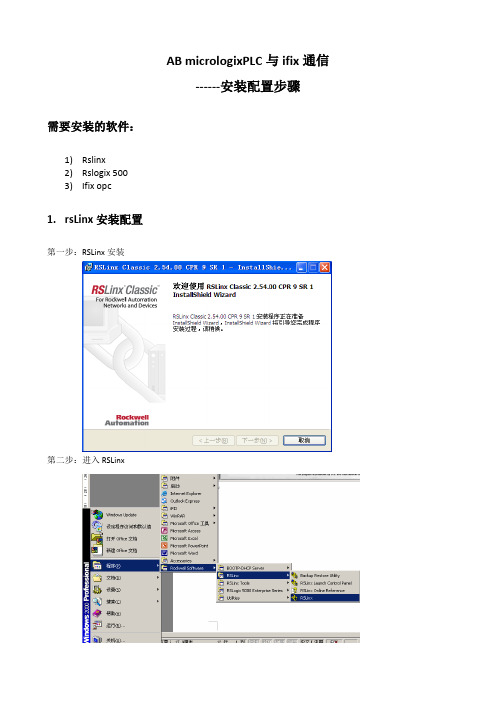
AB micrologixPLC与ifix通信------安装配置步骤需要安装的软件:1)Rslinx2)Rslogix 5003)Ifix opc1.rsLinx安装配置第一步:RSLinx安装第二步:进入RSLinx第三步:配置IP地址1.配置驱动2.选择Ethernet devices3. 4.把PLC的IP增加到网络中5.通过以太网模块读到CPU第四步:验证RSLINX是否正常打开rslinx,找到相应PLC ip找到在RSLogix500中查看的变量,看看在RSLinx中是否变量显示正常关闭DataMonitor,再右击PLC,选择Configure New DDE/OPC Topic在新弹出的界面可更改Topic名称,点击OK点击Yes更新Topic下面可以通过RSLinx自带的OPC Client工具检测RSLinx OPC服务器是否正常读取PLC的数值通过开设菜单找到OPC Test Client选择新建OPC选择RSLinx OPC Server服务器,点击OK新建一个Group,点击OK可以在左下方找到刚才新建的Topic,随意添加一个PLC变量点击OK,然后可以看到可以正常监控到这个PLC变量值,此时说明RSLinx的OPC功能正常使用。
之后可以通过第三方上位机监控软件通过RSLinx OPC Server来监控PLC中的变量值。
2.rsLogix500安装配置第一步:rsLogix500安装输入专业版序列号授权:拷贝到U盘,然后点击执行,然后移到C盘进入rslogix 500:点击通讯,配置,如下图,选择Rslinx中配置好的PLC。
新建工程,选择1400系列PLC3.OPC安装配置以太网接口读写PLC,需要安装ifix opc驱动。
第一步,安装OPC驱动第二步:OPC建立项目OPC进入OPC后新建一个SEREVER.并点击ENABLE.选择Rslinx OPC Server新建一个group并点击ENABLE.新建一个item(名字可以改为你希望的标签名)并点击Browse Server.点击BROWSE SERVER从在线CPU中选取所要得I/O地址.如果在ENABLE IFIX PDB TAG AUTO 前点对勾,此点将以ITEM1的名称进入数据库.重新起名后点击ABC 加入数据库.之后在PDB中建点即可。
AXP392 开发板用户手册说明书

Titan2FPGA开发平台用户手册AXP392开发板AXP392开发板用户手册2/39芯驿电子科技(上海)有限公司文档版本控制文档版本修改内容记录REV1.0创建文档AXP392开发板用户手册目录文档版本控制 (2)目录 (3)一、开发板简介 (5)二、P390核心板 (7)(一)简介 (7)(二)FPGA芯片 (8)(三)DDR4 (9)(四)QSPI Flash (14)(五)时钟配置 (15)(六)LED灯 (17)(七)电源 (18)(八)结构图 (19)(九)连接器管脚定义 (19)三、扩展板 (28)(一)简介 (28)(一)光纤接口 (28)(二)PCIe插槽 (30)(三)SDI输出接口 (32)(四)SDI输入接口 (33)(五)USB转串口 (33)(六)SD卡槽 (34)(七)40针扩展口 (35)(八)按键和LED灯 (37)(九)JTAG调试口 (38)(十)电源 (38)(十一)结构尺寸图 (39)3/39AXP392开发板用户手册4/39芯驿电子科技(上海)有限公司芯驿电子科技(上海)有限公司基于紫光同创FPGA Titan2开发平台的开发板(型号:AXP392)正式发布了,为了让您对此开发平台可以快速了解,我们编写了此用户手册。
这款Titan2FPGA 开发平台采用核心板加扩展板的模式,方便用户对核心板的二次开发利用。
核心板使用紫光同创的TITAN2芯片PG2T390HFFBG900的解决方案,挂载了4片2GB 的高速DDR4SDRAM 芯片和1片128Mb 的QSPI FLASH 芯片。
在底板设计上我们为用户扩展了丰富的外围接口,比如1个PCIex8接口、4路光纤接口、2路SDI 输出接口、2路SDI 输入接口、1路UART 串口接口、1路SD 卡接口、2个40针扩展接口等等。
满足用户各种高速数据交换,数据存储,视频传输处理以及工业控制的要求,是一款"专业级“的FPGA 开发平台。
2016年微芯片技术有限公司PIC24FJ XLP蓝牙低功耗互联网络设备示例用户指南说明书
IoT DemoUser’s GuideInformation contained in this publication regarding device applications and the like is provided only for your convenience and may be superseded by updates. It is your responsibility to ensure that your application meets with your specifications.MICROCHIP MAKES NO REPRESENTATIONS OR WARRANTIES OF ANY KIND WHETHER EXPRESS OR IMPLIED, WRITTEN OR ORAL, STATUTORY OR OTHERWISE, RELATED TO THE INFORMATION,INCLUDING BUT NOT LIMITED TO ITS CONDITION,QUALITY , PERFORMANCE, MERCHANTABILITY OR FITNESS FOR PURPOSE . Microchip disclaims all liability arising from this information and its use. Use of Microchip devices in life support and/or safety applications is entirely at the buyer’s risk, and the buyer agrees to defend, indemnify and hold harmless Microchip from any and all damages, claims,suits, or expenses resulting from such use. No licenses are conveyed, implicitly or otherwise, under any Microchip intellectual property rights unless otherwise stated.Note the following details of the code protection feature on Microchip devices:•Microchip products meet the specification contained in their particular Microchip Data Sheet.•Microchip believes that its family of products is one of the most secure families of its kind on the market today, when used in the intended manner and under normal conditions.•There are dishonest and possibly illegal methods used to breach the code protection feature. All of these methods, to ourknowledge, require using the Microchip products in a manner outside the operating specifications contained in Microchip’s Data Sheets. Most likely, the person doing so is engaged in theft of intellectual property.•Microchip is willing to work with the customer who is concerned about the integrity of their code.•Neither Microchip nor any other semiconductor manufacturer can guarantee the security of their code. Code protection does not mean that we are guaranteeing the product as “unbreakable.”Code protection is constantly evolving. We at Microchip are committed to continuously improving the code protection features of our products. Attempts to break Microchip’s code protection feature may be a violation of the Digital Millennium Copyright Act. If such acts allow unauthorized access to your software or other copyrighted work, you may have a right to sue for relief under that Act.Microchip received ISO/TS-16949:2009 certification for its worldwide headquarters, design and wafer fabrication facilities in Chandler and Tempe, Arizona; Gresham, Oregon and design centers in California and India. The Company’s quality system processes and procedures are for its PIC ® MCUs and dsPIC ® DSCs, K EE L OQ ® code hoppingdevices, Serial EEPROMs, microperipherals, nonvolatile memory and analog products. In addition, Microchip’s quality system for the designand manufacture of development systems is ISO 9001:2000 certified.TrademarksThe Microchip name and logo, the Microchip logo, AnyRate, dsPIC, FlashFlex, flexPWR, Heldo, JukeBlox, KeeLoq,KeeLoq logo, Kleer, LANCheck, LINK MD, MediaLB, MOST, MOST logo, MPLAB, OptoLyzer, PIC, PICSTART, PIC32 logo, RightTouch, SpyNIC, SST, SST Logo, SuperFlash and UNI/O are registered trademarks of Microchip Technology Incorporated in the U.S.A. and other countries.ClockWorks, The Embedded Control Solutions Company, ETHERSYNCH, Hyper Speed Control, HyperLight Load, IntelliMOS, mTouch, Precision Edge, and QUIET-WIRE are registered trademarks of Microchip Technology Incorporated in the U.S.A.Analog-for-the-Digital Age, Any Capacitor, AnyIn, AnyOut, BodyCom, chipKIT, chipKIT logo, CodeGuard, dsPICDEM, , Dynamic Average Matching, DAM, ECAN, EtherGREEN, In-Circuit Serial Programming, ICSP , Inter-Chip Connectivity, JitterBlocker, KleerNet, KleerNet logo, MiWi, motorBench, MPASM, MPF, MPLAB Certified logo, MPLIB, MPLINK, MultiTRAK, NetDetach, Omniscient Code Generation, PICDEM, , PICkit, PICtail,PureSilicon, RightTouch logo, REAL ICE, Ripple Blocker, Serial Quad I/O, SQI, SuperSwitcher, SuperSwitcher II, Total Endurance, TSHARC, USBCheck, VariSense, ViewSpan, WiperLock, Wireless DNA, and ZENA are trademarks of Microchip Technology Incorporated in the U.S.A. and other countries.SQTP is a service mark of Microchip Technology Incorporated in the U.S.A.Silicon Storage Technology is a registered trademark of Microchip Technology Inc. in other countries.GestIC is a registered trademarks of Microchip Technology Germany II GmbH & Co. KG, a subsidiary of Microchip Technology Inc., in other countries.All other trademarks mentioned herein are property of their respective companies.© 2016, Microchip Technology Incorporated, Printed in the U.S.A., All Rights Reserved. ISBN:PIC24FJ IoT DEMO USER’S GUIDEPreface ...........................................................................................................................5Chapter 1. Introduction1.1 Overview ......................................................................................................111.2 PIC® Microcontrollers with XLP Technology ................................................111.3 Microchip RN4020 Module ...........................................................................111.4 Android Application .. (12)Chapter 2. Hardware2.1 Hardware Requirements ..............................................................................132.2 Hardware Connections (15)Chapter 3. Demo Instructions3.1 Installing Android Application on SmartPhone or Tablet ..............................173.2 Establishing Connection between Android Application and RN4020 Module ..173.3 LED Control ..................................................................................................193.4 Switch Status ................................................................................................193.5 128-bit AES Encryption ................................................................................203.6 128-bit AES Decryption .. (20)Chapter 4. Power SavingWorldwide Sales and Service ....................................................................................23PIC24FJ IoT Demo User’s GuidePIC24FJ IoT DEMO USER’S GUIDEThis preface contains general information that will be useful to know before using thePIC24FJ IoT Demo. Topics discussed in this preface include:•Document Layout•Conventions Used in this Guide•Warranty Registration•Recommended Reading•The Microchip Web Site•Development Systems Customer Change Notification Service•Customer Support•Document Revision HistoryDOCUMENT LAYOUTThis user’s guide describes how to use the PIC24FJ IoT Demo. The document is orga-nized as follows:•Chapter 1. “Introduction” – This chapter introduces the reader to the PIC24FJIoT Demo.•Chapter 2. “Hardware” – This chapter discusses the hardware requirements andtheir connections for the demo.•Chapter 3. “Demo Instructions” – This chapter provides instructions toestablish connection between the Android application and the RN4020 module.•Chapter 4. “Power Saving” – This chapter discusses the power saving aspect ofthe demo.CONVENTIONS USED IN THIS GUIDEThis manual uses the following documentation conventions:WARRANTY REGISTRATIONPlease complete the enclosed Warranty Registration Card and mail it promptly.Sending in the Warranty Registration Card entitles users to receive new productupdates. Interim software releases are available at the Microchip web site. RECOMMENDED READINGThis user’s guide describes PIC24FJ IoT Demo. The device-specific data sheets containcurrent information on programming the specific microcontroller or digital signal controllerdevices. Other useful documents are listed below. The following Microchip documents areavailable and recommended as supplemental reference resources.For more information on PIC24FJ devices, Cypto module or RN4020 module refer to:•/PIC24FJ128GB204•/PIC24FJ128GA204•/PIC24FJ256GB410•/RN4020•AN1861 “Bluetooth® Smart Communication Using Microchip RN4020 Module and16-bit PIC® Microcontroller“THE MICROCHIP WEB SITEMicrochip provides online support via our web site at . This website is used as a means to make files and information easily available to customers.Accessible by using your favorite Internet browser, the web site contains the followinginformation:•Product Support – Data sheets and errata, application notes and sampleprograms, design resources, user’s guides and hardware support documents,latest software releases and archived software•General Technical Support – Frequently Asked Questions (FAQs), technicalsupport requests, online discussion groups, Microchip consultant programmember listing•Business of Microchip – Product selector and ordering guides, latest Microchippress releases, listing of seminars and events, listings of Microchip sales offices,distributors and factory representativesDEVELOPMENT SYSTEMS CUSTOMER CHANGE NOTIFICATION SERVICEMicrochip’s customer notification service helps keep customers current on Microchipproducts. Subscribers will receive e-mail notification whenever there are changes,updates, revisions or errata related to a specified product family or development tool ofinterest.To register, access the Microchip web site at , click on CustomerChange Notification and follow the registration instructions.The Development Systems product group categories are:•Compilers – The latest information on Microchip C compilers and other languagetools. These include the MPLAB® C compiler; MPASM™ and MPLAB® 16-bitassemblers; MPLINK™ and MPLAB® 16-bit object linkers; and MPLIB™ andMPLAB® 16-bit object librarians.•Emulators – The latest information on the Microchip MPLAB® REAL ICE™in-circuit emulator.•In-Circuit Debuggers – The latest information on the Microchip in-circuitdebugger, MPLAB® ICD 3.•MPLAB IDE – The latest information on Microchip MPLAB® IDE, the Windows®Integrated Development Environment for development systems tools. This list isfocused on the MPLAB® IDE, MPLAB® SIM simulator, MPLAB® IDE Project Man-ager and general editing and debugging features.•Programmers – The latest information on Microchip programmers. These includethe MPLAB® PM3 device programmer and the PICkit™ 3 developmentprogrammers.CUSTOMER SUPPORTUsers of Microchip products can receive assistance through several channels:•Distributor or Representative•Local Sales Office•Field Application Engineer (FAE)•Technical SupportCustomers should contact their distributor, representative or FAE for support. Localsales offices are also available to help customers. A listing of sales offices andlocations is included in the back of this document.Technical support is available through the web site at: DOCUMENT REVISION HISTORYRevision A (July 2016)This is the initial released version of the document.NOTES:PIC24FJ IoT DEMO USER’S GUIDE1.1OVERVIEWBluetooth® has emerged as a standard of choice for connecting local embedded appli-cations through a router, smartphone or tablet. Today, Bluetooth is known to provideeasy and temporary connectivity to smartphones and tablets, and is supported in manyAndroid® and iOS® applications. Many applications only need simple command andcontrol, or a quick status update from a sensor. By catering to these needs BluetoothLow Energy (BLE) has evolved to support these low-duty cycle applications.However, when the application is a simple command and control, the power consump-tion is also expected to be as low as possible. Power consumption has become one ofthe foremost concerns for embedded system designers. It is important that a microcon-troller not only consumes as little power as possible, but also provides features thatallow for minimal power consumption in the rest of the design as well. Microchip’seXtreme Low Power PIC® Microcontrollers and RN4020 BLE module help in achievinglow power consumption.This demonstration shows the simple communication between the RN4020 moduleand a BLE supporting smartphones or tablets. The RN4020 module is controlled by thePIC24FJ MCU which also includes a hardware Crypto engine used for AES encryptionin the demonstration. The demonstration is built using standard development tools fromMicrochip including the Explorer 16 Board, PIC24FJ Controller Plug-In Module (PIM),and BLE PICtail TM Plus Daughter Card. These readily available tools helps to easilyreplicate the demo. The demo is supported by the MCU firmware and an applicationthat will run on an Android phone or tablet.1.2PIC® MICROCONTROLLERS WITH XLP TECHNOLOGYAs more electronic applications require low power or battery power, energy conserva-tion becomes paramount. Today’s applications must consume little power and, inextreme cases, last for up to 15–20 years while running from a single battery. To enableapplications like these, products with Microchip’s eXtreme Low Power (XLP) Technol-ogy offer the industry’s lowest currents, where extreme low power applications spend90% to 99%of their time.The PIC24FJ device used in this demo has an integrated hardware Crypto engine. TheCrypto engine is intended to accelerate applications that need cryptographic functions.The Crypto engine supports AES and DES/TDES ciphers. A 128-bit AES is shown inthis demo.1.3MICROCHIP RN4020 MODULEThe BLE, also known as Bluetooth Smart, is intended for low-duty cycle devices thatsupport low-data throughput and can operate for a longer duration compared to otherprotocols from a coin cell battery. BLE operates in the same spectrum band (i.e., 2.400GHz to 2.4835 GHz ISM band) as Classic Bluetooth technology, but uses a differentset of channels and different modulation techniques.For additional information related to Bluetooth and its specifications, refer to “BluetoothCore Specification V4.0” from the following web site:The Microchip RN4020 is a fully-certified Bluetooth Version 4.1 module for adding low-power wireless capability to applications and products.1.4ANDROID APPLICATIONThe Android application (16-bit XLP BLE AES Demo) interacts with the RN4020 BLEPICtail plus module. The smart phone or tablet in which the application is installedshould support Bluetooth 4.0 or newer. The application is compatible with Android 5.0lollipop and lower versions.1.4.1Main Functionality of the IoT Application:•Discover BLE devices nearby•Toggle the LEDs on the Explorer 16 Board•Reflect the switch state of the Explorer 16 Board•Receive 128-bit AES encrypted data (Cipher Text) from the PIC24FJ device for agiven plain text•Receive 128-bit AES decrypted data from the PIC24FJ device for a given CipherTextPIC24FJ IoT DEMO USER’S GUIDE2.1HARDWARE REQUIREMENTSHardware requirements to run this demo are as follows:1.Power Supply (9V)https:///ProductSearch.aspx?Keywords=AC0020142.One of the following microcontrollers is required for the Explorer 16 Board:-PIC24FJ128GB204 PIM (Part # MA240036)-PIC24FJ128GA204 PIM (Part # MA240037)-PIC24FJ256GB410 PIM (Part # MA240038)The device needs to be programmed on the Explorer 16 Board with supportedhex file which can be downloaded from:/PIC24IoTDemoTo learn more about loading a hex file, view the following video:https:///watch?v=pEMORwwuyosFIGURE 2-1:MICROCONTROLLERSThe jumper settings on the PIMs for this demo are listed in Table 2-13.RN4020 Bluetooth PICtail Daughter Card with JP1 jumper placed (Part # RN-420-PICtail)4.Explorer 16 Development Board (Part # DM240001) – Both PIM and PICtailDaughter Card plug directly into the Explorer 16 Board2.2HARDWARE CONNECTIONS1.Mount the RN4020 Bluetooth PICtail Daughter Card on the Explorer 16 Develop-ment Board’s PICtail Plus slot.Ensure that the Pin No1 of PICtail is aligned to Pin No1 of the PICtail Plus slot asMount the PIC24FJ PIM in the U1 socket as shown in the following images:2016 Microchip Technology Inc.DS00000A-page 153.On the Explorer 16 Board ensure to:Connect Jumper J7 to PIC24 endMount Jumper JP2 as shown in the following imagePower up the Explorer 16 Board using a 9V power supplyPIC24FJ IoT DEMO USER’S GUIDE3.1INSTALLING ANDROID APPLICATION ON SMARTPHONE OR TABLET1.Enable “Unknown Sources” on Android - to enable Unknown Sources go toSettings > Security and check the box next to “Unknown Sources”2.Download the .apk file “com.microchip.iotdemo-2.apk” from:/PIC24IoTDemo3.Install the .apk file4.Navigate to the directory where the .apk file has been downloaded5.Tap the .apk file and an installation dialogue box will pop-up. Select the “Install”button to install the .apk on your Android device.3.2ESTABLISHING CONNECTION BETWEEN ANDROID APPLICATION ANDRN4020 MODULE1.On power-up of the Explorer 16 Board the following is observed:The LED D7 starts flashing every 0.5 secondsWhile the application runs the following events occur:a)If the Bluetooth is OFF, the application will request to turn ON the BluetoothSelecting IoT_BLE establishes connection between the Android phone or tablet and RN4020 module on the Explorer 16 Board.b)The application will scan for the BLE enabled modules in the vicinity. If found,This also opens the interactive screen on the tablet or smartphone.d)Connection status is reflected with CONN LED ON in RN4020 PICtail3.3LED CONTROLAs shown in the following images the application controls turning ON and OFF of theLED D9 and D8 independently on the Explorer 16 Board. This demonstrates controllingan end application remotely from the phone or tablet.3.4SWITCH STATUSThe application also reflects the status of S3 and S4 switches of the Explorer 16 Board.Changing the status of the switches on the Explorer 16 Board will reflect in the ON/OFFstatus changing on the application. This demonstrates communication of sensor infor-mation or data from an end application to a phone or tablet.2016 Microchip Technology Inc.DS00000A-page 193.5128-BIT AES ENCRYPTIONTo protect the data in the end application, the data can be encrypted locally, before being sent to/from the board (end application) to the phone or tablet, and sometimes on to a cloud-based storage.For 128-bit AES encryption:1.On the application, in the “Plain Text” field enter the hex numbers to beencrypted.Plain text can be a maximum of 32 characters and any text lesser than 32 char-acters will be appended with 0s by the application.Similar to the one available in the following link, there are online tools for AES encryption:/2.After entering the data to be encrypted on the application, select the “Encrypt”button.The PIC24FJ device will encrypt the data by using the default 128-bit Key “95 A8 EE 8E 89 97 9B 9E FD CB C6 EB 97 97 52 8D”.Encrypted data will be displayed in “Cipher Text” field.3.6128-BIT AES DECRYPTIONFor 128-bit AES decryption:1.Enter the hex numbers to be decrypted in the “Cipher Text” field.Cipher text can be a maximum of 32 characters and any text lesser than 32 char-acters will be appended with 0s by the application.2.After entering the data to be decrypted, select the “Decrypt” button.The PIC24FJ MCU will decrypt the data and it will be displayed in the “DecryptedPIC24FJ IoT DEMO USER’S GUIDEIf there is no activity, either in the Android application or on the Explorer 16 Board, for 1 minute, the BLE module and the PIC24FJ device enter Seep mode to save power. Simultaneously, the following events occur:•The WAKE LED of the BLE module will turn OFF•The LED D7 on the Explorer 16 Board turns OFFThe RN4020 and PIC24FJ will wake up by asserting either the S3 or S4 switch on theAMERICAS Corporate Office2355 West Chandler Blvd. Chandler, AZ 85224-6199 Tel: 480-792-7200Fax: 480-792-7277 Technical Support: / supportWeb Address: AtlantaDuluth, GATel: 678-957-9614Fax: 678-957-1455 Austin, TXTel: 512-257-3370 Boston Westborough, MATel: 774-760-0087Fax: 774-760-0088 ChicagoItasca, ILTel: 630-285-0071Fax: 630-285-0075 Cleveland Independence, OHTel: 216-447-0464Fax: 216-447-0643 DallasAddison, TXTel: 972-818-7423Fax: 972-818-2924 DetroitNovi, MITel: 248-848-4000 Houston, TXTel: 281-894-5983 Indianapolis Noblesville, INTel: 317-773-8323Fax: 317-773-5453Los AngelesMission Viejo, CATel: 949-462-9523Fax: 949-462-9608New York, NYTel: 631-435-6000San Jose, CATel: 408-735-9110 Canada - TorontoTel: 905-695-1980Fax: 905-695-2078ASIA/PACIFICAsia Pacific OfficeSuites 3707-14, 37th FloorTower 6, The GatewayHarbour City, KowloonHong KongTel: 852-2943-5100Fax: 852-2401-3431Australia - SydneyTel: 61-2-9868-6733Fax: 61-2-9868-6755China - BeijingTel: 86-10-8569-7000Fax: 86-10-8528-2104China - ChengduTel: 86-28-8665-5511Fax: 86-28-8665-7889China - ChongqingTel: 86-23-8980-9588Fax: 86-23-8980-9500China - DongguanTel: 86-769-8702-9880China - GuangzhouTel: 86-20-8755-8029China - HangzhouTel: 86-571-8792-8115Fax: 86-571-8792-8116China - Hong Kong SARTel: 852-2943-5100Fax: 852-2401-3431China - NanjingTel: 86-25-8473-2460Fax: 86-25-8473-2470China - QingdaoTel: 86-532-8502-7355Fax: 86-532-8502-7205China - ShanghaiTel: 86-21-5407-5533Fax: 86-21-5407-5066China - ShenyangTel: 86-24-2334-2829Fax: 86-24-2334-2393China - ShenzhenTel: 86-755-8864-2200Fax: 86-755-8203-1760China - WuhanTel: 86-27-5980-5300Fax: 86-27-5980-5118China - XianTel: 86-29-8833-7252Fax: 86-29-8833-7256China - XiamenTel: 86-592-2388138Fax: 86-592-2388130China - ZhuhaiTel: 86-756-3210040Fax: 86-756-3210049India - BangaloreTel: 91-80-3090-4444Fax: 91-80-3090-4123India - New DelhiTel: 91-11-4160-8631Fax: 91-11-4160-8632India - PuneTel: 91-20-3019-1500Japan - OsakaTel: 81-6-6152-7160Fax: 81-6-6152-9310Japan - TokyoTel: 81-3-6880- 3770Fax: 81-3-6880-3771Korea - DaeguTel: 82-53-744-4301Fax: 82-53-744-4302Korea - SeoulTel: 82-2-554-7200Fax: 82-2-558-5932 or82-2-558-5934Malaysia - Kuala LumpurTel: 60-3-6201-9857Fax: 60-3-6201-9859Malaysia - PenangTel: 60-4-227-8870Fax: 60-4-227-4068Philippines - ManilaTel: 63-2-634-9065Fax: 63-2-634-9069SingaporeTel: 65-6334-8870Fax: 65-6334-8850Taiwan - Hsin ChuTel: 886-3-5778-366Fax: 886-3-5770-955Taiwan - KaohsiungTel: 886-7-213-7828Taiwan - TaipeiTel: 886-2-2508-8600Fax: 886-2-2508-0102Thailand - BangkokTel: 66-2-694-1351Fax: 66-2-694-1350Austria - WelsTel: 43-7242-2244-39Fax: 43-7242-2244-393Denmark - CopenhagenTel: 45-4450-2828Fax: 45-4485-2829France - ParisTel: 33-1-69-53-63-20Fax: 33-1-69-30-90-79Germany - DusseldorfTel: 49-2129-3766400Germany - KarlsruheTel: 49-721-625370Germany - MunichTel: 49-89-627-144-0Fax: 49-89-627-144-44Italy - MilanTel: 39-0331-742611Fax: 39-0331-466781Italy - VeniceTel: 39-049-7625286Netherlands - DrunenTel: 31-416-690399Fax: 31-416-690340Poland - WarsawTel: 48-22-3325737Spain - MadridTel: 34-91-708-08-90Fax: 34-91-708-08-91Sweden - StockholmTel: 46-8-5090-4654UK - WokinghamTel: 44-118-921-5800Fax: 44-118-921-5820 Worldwide Sales and Service06/23/16。
防止Portal弹出的应用程序认证方法及系统、无线接入设备[发明专利]
![防止Portal弹出的应用程序认证方法及系统、无线接入设备[发明专利]](https://img.taocdn.com/s3/m/9b06e7a2e45c3b3566ec8b54.png)
专利名称:防止Portal弹出的应用程序认证方法及系统、无线接入设备
专利类型:发明专利
发明人:张晓波
申请号:CN201710546322.X
申请日:20170706
公开号:CN107294995A
公开日:
20171024
专利内容由知识产权出版社提供
摘要:本发明公开了一种防止Portal弹出的应用程序认证方法及系统、无线接入设备,该方法包括步骤:S1.对新接入终端开启短暂的数据放行;S2.接收所述终端中应用程序发送的认证状态查询报文,并向所述终端发送认证状态查询结果;S3.若所述终端为未认证状态,停止对所述终端的数据放行,并向所述终端发送认证服务器地址信息;S4.接收认证服务器发送的终端应用程序认证通过的通知,对所述终端开启数据放行。
本发明提供了一种防止Portal弹出的应用程序认证方法及系统,在应用程序中直接连接无线接入设备的同时,可以有效的避免captive portal功能自动弹出portal认证页面。
申请人:上海斐讯数据通信技术有限公司
地址:201616 上海市松江区思贤路3666号
国籍:CN
代理机构:杭州千克知识产权代理有限公司
更多信息请下载全文后查看。
一种基于fpga的cx9261芯片配置方法

一种基于fpga的cx9261芯片配置方法下载温馨提示:该文档是我店铺精心编制而成,希望大家下载以后,能够帮助大家解决实际的问题。
文档下载后可定制随意修改,请根据实际需要进行相应的调整和使用,谢谢!并且,本店铺为大家提供各种各样类型的实用资料,如教育随笔、日记赏析、句子摘抄、古诗大全、经典美文、话题作文、工作总结、词语解析、文案摘录、其他资料等等,如想了解不同资料格式和写法,敬请关注!Download tips: This document is carefully compiled by the editor. I hope that after you download them, they can help you solve practical problems. The document can be customized and modified after downloading, please adjust and use it according to actual needs, thank you!In addition, our shop provides you with various types of practical materials, such as educational essays, diary appreciation, sentence excerpts, ancient poems, classic articles, topic composition, work summary, word parsing, copy excerpts, other materials and so on, want to know different data formats and writing methods, please pay attention!FPGA技术在现代电子行业中扮演着越来越重要的角色,而CX9261芯片作为一种基于FPGA的解决方案,其配置方法对于设备性能的优化和功能实现至关重要。
ccp协议 bootload

ccp协议 bootload
CCP协议(CAN Calibration Protocol)是一种用于CAN总线上的诊断和校准的通信协议。
它允许外部设备与汽车电子控制单元(ECU)进行通信,以便进行诊断、校准和参数设置。
CCP协议通常用于汽车行业,特别是在发动机控制单元(ECU)和其他车辆控制系统的开发和测试过程中。
Bootload是指在计算机或嵌入式系统启动过程中加载操作系统或应用程序的过程。
在嵌入式系统中,bootload通常指的是引导加载程序,它负责从存储设备(如闪存、SD卡等)中加载操作系统或应用程序到系统内存中并启动。
Bootload通常包括引导加载程序的设计、开发和部署。
从CCP协议和bootload的角度来看,它们在汽车电子控制系统中扮演着不同的角色。
CCP协议用于与汽车ECU进行通信,而bootload则用于嵌入式系统的启动过程。
在汽车行业中,这两个概念通常会同时涉及到,因为在汽车电子控制系统的开发和测试过程中,需要通过CCP协议与ECU进行通信,并且可能需要使用bootload来加载和启动相应的软件。
总的来说,CCP协议和bootload在汽车电子控制系统的开发和测试中扮演着重要的角色,它们之间有着密切的联系,但又各自拥有不同的功能和应用场景。
在实际应用中,需要根据具体的情况来合理地使用和配置它们,以确保汽车电子控制系统的稳定性和可靠性。
Cisco兼容40G QSFP+ 光模块用户指南说明书
User GuideTN-QSFP-40G-xxCisco Compatible 40G QSFP+Optical Transceivers•High capacity: up to 44.4 Gbps per module•Compliant with SFF 8436 QSFP+ MSA•Single +3.3 V Power Supply•RoHS Compliant (all models)•Low Power Dissipation : SR4< 1.5 Watts, LR4 < 3.5w•Digital Diagnostic Monitoring (DMI and DDMI)•Class 1 Laser International Safety Standard IEC 60825 Compliant•40GBase-SR4: 4 lanes, up to 11.1Gbps per lane, Standard MPO connector•40GBase-LR4: 4 wavelength CWDM Mux/Demux design, up to 11.1Gbps per wavelength, Duplex LC connectorContentsIntroduction (1)Description (2)Ordering Information (2)Specifications and Standards (2)Optical Specifications (2)Application: Fiber Connection with QSFP+ (3)QSFP+ Unpacking (3)QSFP+ Installation (4)Cautions (4)Installing a QSFP+ Module (4)Fiber Cable Physical Characteristics (5)Connecting Fiber Cables (5)Removing a QSFP+ Module (5)Diagnostic Monitoring Interface (DMI) (6)Digital Diagnostics Monitoring Interface (DDMI) (7)For More Information (8)Contact Us (8)Compliance Information (9)Record of Revisions (10)IntroductionThe Transition Networks TN-QSFP-40G-xx series 40G QSFP+ optical transceivers are designed to install in any QSFP+ port allowing for 40GBase-X interfaces to the network through the QSFP+ connector.The TN-QSFP-40G-xx transceivers are Cisco compatible* and are designed for bi-directional serial-optical data communication such as 40G Ethernet.DescriptionTransition Networks’ QSFP+ modules fully comply with the Multi-Sourcing Agreement (MSA).This compliance allows our QSFP+ modules to be used in all other MSA compliant QSFP+ platforms. In addition, TN QSFP+ modules are also compatible with all Cisco QSFP+ based routers and switches, as well as Cisco’s IOS software. TN QSFP+ modules are not Cisco OEM brand modules. Ordering InformationProduct Number DescriptionTN-QSFP-40G-LR4 QSFP+ 40GBase-LR4, 1271nm, 1291nm, 1311nm, 1331nm, single mode (LC)[10km/6.2mi.] Link Budget: 7.0 dBTN-QSFP-40G-SR4 QSFP+ 40GBase-SR4, 850nm multimode (MPO) [400m/1313ft. on OM4, 300m/985ft. on OM3] Link Budget: 2.3 dBTN-QSFP-40G-LR4-3 QSFP+ 40GBase-LR4, 1271nm, 1291nm, 1311nm, 1331nm single mode (LC)[30km/18.7mi.] Link Budget: 9.0 dBSpecifications and StandardsThe TN-QSFP-40G-xx was designed to meet these standards and specifications:Optical SpecificationsThe Optical Specs for all Transition Networks’ SFPs are available on our Optical Devices webpage.Application: Fiber Connection with QSFP+Applications include: 40G Ethernet, 10G Ethernet, and Data Center Aggregation Connection.QSFP+UnpackingBefore you start installing the TN-QSFP-40G-xx, verify that the package contains the following items: o One TN-QSFP-40G-xx SFPo Two protective foam pieceso One Documentation PostcardNotify your sales representative immediately if any of the above items is missing or damaged. Save the packaging for possible future use.The optical ports of the QSFP+ transceiver must be terminated with an optical connector or with a dust plug. The QSFP+ transceiver must be operated within the specified temperature and voltage limits.QSFP+ InstallationCautions•The QSFP+ tranceiver module is keyed to only be installed one way. However, if forced the wrong way, damage may occur. •Avoid getting dust or other contaminants into the fiber bore of the QSFP+ transceiver module. •Clean the optic surfacees of the optical fiber before you plug them back in to the optical bores of another QSFP+ tranceiver module. • Each port must match the wavelength specifications on the other end of the cable, and the cablemust not exceed the specified cable length for reliable communications.Installing a QSFP+ Module1. Attach an ESD-preventive wrist strap to your wrist and to the ESD ground connector or a bare metalsurface on your chassis.2. Remove the QSFP+ transceiver module from its protective packaging. Note: Do not remove theoptical bore dust plugs until directed to do so in a later procedure.3. Check the slot orientation. Note that for some devices (e.g., S4224) some slots are “upside down”compared to other slots.4. Position the QSFP+device at the desired installation slot, with the label facing correctly.5. Carefully slide the QSFP+ device into the slot, aligning it with the internal installation guides.Triangleindicates bottomof SFP cageSFP Module Label side top of SFP moduleBaleClasp SwitchFully Inserted SFPSwitch 6. Ensure that the QSFP+device is firmly seated against the internal mating connector. To verify that theQSFP+ is seated and latched properly. a ) Grasp the QSFP+ by the sides and try to remove it without releasing the latch. b) If the QSFP+ can not be removed, it is installed and seated properly. If the QSFP+ can be removed, reinsert it and press harder with your thumb; repeat if necessary until it is latched securely into the socket.7. Connect the fiber cable to the fiber port connector of the QSFP+ device. Make sure the QSFP+release latch is in the up (closed) position when you insert the cable connector into the QSFP+.8. Remove the dust plug from the connector. Save the dust plug for future use.9. Attach an appropriate cable into the QSFP+ module port.10. Attach the other end of the cable into the other device.11. Observe the status LED(s). See the related manual for details.Fiber Cable Physical CharacteristicsThe fiber cable physical characteristics must meet or exceed IEEE 802.3ae specifications:•Single mode fiber (recommended): 9 μm•Multimode fiber (recommended): 62.5/125 μm•Multimode fiber (optional): 100/140, 85/140, 50/125 μmWarning: Visible and invisible laser radiation when open. DO NOT stare into laser beam or view directly with optical instruments. Failure to observe this warning could result in damage to your eyes or blindness. Connecting Fiber CablesTo install the fiber cable, do the following:1. Locate the appropriate fiber cable.2. Install the cable as shown below.Removing a QSFP+ModuleCaution: Be careful when removing the QSFP+ from a device. Some QSFP+ transceiver module temperatures may exceed 160°F (70°C) and be too hot to touch with bare hands. Note: Do not remove and replace the QSFP+ modules more often than necessary; excessive QSFP+ removing and replacing can shorten the useful life of the QSFP+.1. Attach an ESD-preventive wrist strap to your wrist and to the ESD ground connector or a bare metalsurface on your chassis.2. For future reattachment of fiber-optic cables, note which connector plug is send (TX) and which isreceive (RX).3. Remove the QSFP+ transceiver module:a. If the QSFP+ transceiver module has an actuator button latch, gently press the actuator buttonon the front of the QSFP+ transceiver module until it clicks and the latch mechanism releases the QSFP+ transceiver module from the socket connector. Grasp the actuator button between your thumb and index finger, and carefully pull the QSFP+ transceiver module straight out of the module slot.b. If the QSFP+ transceiver module has a bail clasp latch, pull the latch out and down to eject theQSFP+ transceiver module from the socket connector. If the bail clasp latch is obstructed and you cannot use your index finger to open it, use a small, flat-blade screwdriver or other long, narrow instrument to open the bail clasp latch. Grasp the QSFP+ transceiver module between your thumb and index finger, and carefully remove it from the socket.4. Replace the Dust Plug.5. Place the removed QSFP+ transceiver module in an antistatic bag or other protective package.Diagnostic Monitoring Interface (DMI)The following DMI port screen and explanation table contains brief definitions of the DMI support offered on some QSFP+ transceiver modules. For further information, see the help option on the CPSMM-xxx, SNMP agent, or Transition Networks Focal Point or ION System GUI. Note: This feature is not availableon all devices and may vary between products. See the related manual for more information.DMI Parameter Description DMI Rx PowerMeasured receive optical power in microwatts and in decibels relative to 1mW. DMI Rx PowerAlarmAlarm status of measured receive optical power. DMI Temp Internally measured temperature of transceiver in degrees Celsius and degreesFarenheit.DMI Temp Alarm Alarm status for internally measured temperature of the transceiver.DMI Bias Current Measured transmit bias current in microamperes.DMI Bias Alarm Alarm status for measured transmit bias current for the interface.DMI Tx Power Measured transmit power in microwatts and in decibels relative to 1mW. DMI Tx Power Alarm Alarm status of measured transmit power.Rx Power Intrusion Threshold Tells the converter to stop passing traffic when the receive power drops belowthe new threshold. This feature is sometimes referred to as 'Intrusion Detection,' since tapping into a fiber to intercept traffic leads to a reduction in receive power.This value can be entered in microwatts or in decibels relative to 1mW.TN-QSFP+ distances, TX power, RX power, and link budgets can be found on Transition Netwoks’ website, document “SFP/XFP Fiber and Copper Connectors.” See at https:///. The fiber optic transmitters on this device meet Class I Laser safety requirements per IEC-825/CDRH standards and comply with 21 CFR1040.10 and 21CFR1040.11.WARNING: Visible and invisible laser radiation when open. Do not stare into the beam or view the beam directly with optical instruments. Failure to observe this warning could result in an eye injury or blindness. IMPORTANT: Copper based media ports such as Twisted Pair (TP) Ethernet, USB, RS232, RS422, RS485, DS1, DS3, Video Coax, etc., are intended to be connected to intra-building (inside plant) linksegments that are not subject to lightening transients or power faults. Copper-based media ports such as Twisted Pair (TP) Ethernet, USB, RS232, RS422, RS485, DS1, DS3, Video Coax, etc., are NOT to be connected to inter-building (outside plant) link segments that are subject to lightening transients or power faults.Digital Diagnostics Monitoring Interface (DDMI)DDMI (Digital Diagnostics Monitoring Interface) provides enhanced digital DMI for optical transceivers which allows real time access to device operating parameters.This section contains brief definitions of the DDMI support offered on some QSFP+ transceiver modules. For further information, see the help option or User Guide for the S3290, S4140, S4212, and S4224. Note: This feature is not available on all devices and may vary between products.The Transceiver Information and DDMI Information sections are described below. DDMI ParameterDescription DMIRx Power (uW) Intrusion Threshold; a level for Rx Power on the Fiber port. If the DMI read value falls below the preset value, an intrusion is detected, and a trap is generated. The default is 0 uW. The range is 0 - 65,535 uW. PortThe device’s port number. VendorThe QSFP+ vendor’s name (e.g., Transition ). Part NumberThe QSFP+ vendor Part number provided by the QSFP+ vendor (TN-10GSFP-SR ). Serial NumberThe QSFP+ Vendor Serial number provided by the QSFP+ vendor (e.g., 8672105). RevisionThe QSFP+ vendor Revision level for part number provided by the QSFP+ vendor. Data CodeThe vendor's manufacturing date code (e.g ., 2011-08-09). TranseiverThe Transceiver compatibility (e.g., 1000BASE_SX or 10G ). CurrentThe current value of temperature, voltage, TX bias, TX power, and RX power. High Alarm ThresholdThe high alarm threshold value of temperature, voltage, TX bias, TX power, and RX power. High Warn ThresholdThe high warn threshold value of temperature, voltage, TX bias, TX power, and RX power. Low Warn ThresholdThe low warn threshold value of temperature, voltage, TX bias, TX power, and RX power. Low Alarm Threshold The low alarm threshold value of temperature, voltage, TX bias, TX power,and RX power.For More InformationTechnical information in this document is subject to change without notice. For more information see the TN SFP webpage.40 Gigabit Ethernet ("40GbE" or "40G") Port Types (40GBASE-CR4, 40GBASE-KR4, 40GBASE-SR4, 40GBASE-LR4, 40GBASE-ER4, 40GBASE-FR, 40GBASE-T) ITU standards descriptions include:40GBASE-SR4 ("short range") is a port type for multi-mode fiber and uses 850 nm lasers. Its Physical Coding Sublayer 64b/66b PCS is defined in IEEE 802.3 Clause 82 and its Physical Medium Dependent PMD in Clause 86. It uses four lanes of multi-mode fiber delivering serialized data at a rate of 10.3125 Gbit/s per lane. 40GBASE-SR4 has a reach of 100 m on OM3 and 150m on OM4. There is a longer range variant 40GBASE-eSR4 with a reach of 300 m on OM3 and 400 m on OM4. This extended reach is equivalent to the reach of 10GBASE-SR.40GBASE-LR4 ("long range") is a port type for single-mode fiber and uses 1300 nm lasers. Its Physical Coding Sublayer 64b/66b PCS is defined in IEEE 802.3 Clause 82 and its Physical Medium Dependent PMD in Clause 87. It uses four wavelengths delivering serialized data at a rate of 10.3125 Gbit/s per wavelength.The amendment to IEEE Std 802.3-2008 includes changes to IEEE Std 802.3-2008 and adds Clause 80 through Clause 88, Annex 83A through Annex 83C, Annex 85A, and Annex 86A. This amendment includes IEEE 802.3 Media Access Control (MAC) parameters, Physical Layer specifications, and management parameters for the transfer of IEEE 802.3 format frames at 40 Gb/s and 100 Gb/s.EIA SFF-8436 Rev 4.8 section 5.5 Color Coding and Labeling of QSFP+ Modules: An exposed feature of the QSFP+ Module (a feature or surface extending outside of the bezel) shall be color coded as follows: Beige for 850nm, Blue for 1310nm, and White for 1550nm. For more information seeftp:///sff/SFF-8436.PDF.Contact UsTechnical Support: Technical support is available 24-hours a dayUS and Canada: 1-800-260-1312International: 00-1-952-941-7600Main Officetel: +1.952.941.7600 | toll free: 1.800.526.9267 | fax: 952.941.2322******************** | ************************** | ******************************AddressTransition Networks10900 Red Circle DriveMinnetonka, MN 55343, U.S.A.Compliance InformationClass I Laser ComplianceThis product has been tested and found to comply with the limits for FDA Class I laser for IEC60825,EN60825, and 21CFR1040 specifications.Translated Safety WarningsWarning Class I laser product. Advarsel Laserprodukt av klasse I.Waarschuwing Klasse-I laser produkt. Aviso Produto laser de classe I.Varoitus Luokan I lasertuote. ¡Advertencia! Producto láser Clase I.Attention Produit laser de classe I Varning! Laserprodukt av klass I.Warnung Laserprodukt der Klasse I. Aviso Produto a laser de classe I.Avvertenza Prodotto laser di Classe I. Advarsel Klasse I laserprodukt.FCC RegulationsThis equipment has been tested and found to comply with the limits for a Class A digital device, pursuant to Part 15 of the FCC rules. These limits are designed to provide reasonable protection against harmful interference when the equipment is operated in a commercial environment. This equipment generates, uses and can radiate radio frequency energy and, if not installed and used in accordance with the instruction manual, may cause harmful interference to radio communications.Operation of this equipment in a residential area is likely to cause harmful interference, in which case the user will be required to correct the interference at the user's own expense.Canadian RegulationsThis digital apparatus does not exceed the Class A limits for radio noise for digital apparatus set out on the radio interference regulations of the Canadian Department of Communications.Le présent appareil numérique n'émet pas de bruits radioélectriques dépassant les limites applicables aux appareils numériques de la Class A prescrites dans le Règlement sur le brouillage radioélectrique édicté par le ministère des Communications du Canada.European RegulationsWarningThis is a Class A product. In a domestic environment this product may cause radio interference in which case the user may be required to take adequate measures.Achtung !Dieses ist ein Gerät der Funkstörgrenzwertklasse A. In Wohnbereichen können bei Betrieb dieses Gerätes Rundfunkstörungen auftreten. In diesem Fäll is der Benutzer für Gegenmaßnahmen verantwortlich.Attention !Ceci est un produit de Classe A. Dans un environment domestique, ce produit risque de créer desinterférences radioélectriques, il appartiendra alors à l'utilsateur de prende les measures spécifiquesappropriées.In accordance with European Union Directive 2002/96/EC of the European Parliament and of theCouncil of 27 January 2003, Transition Networks will accept post usage returns of this product for proper disposal. The contact information for this activity can be found in the 'Contact Us' portion of this document.Der Anschluss dieses Gerätes an ein öffentlickes Telekommunikationsnetz in den EGMitgliedstaatenverstösst gegen die jeweligen einzelstaatlichen Gesetze zur Anwendung der Richtlinie 91/263/EWG zur Angleichung der Rechtsvorschriften der Mitgliedstaaten über Telekommunikationsendeinrichtungen einschliesslich der gegenseitigen Anerkennung ihrer Konformität.CAUTION: RJ connectors are NOT INTENDED FOR CONNECTION TO THE PUBLICTELEPHONE NETWORK. Failure to observe this caution could result in damage to the publictelephone network.Der Anschluss dieses Gerätes an ein öffentlickes Telekommunikationsnetz in den EGMitgliedstaatenverstösst gegen die jeweligen einzelstaatlichen Gesetze zur Anwendung der Richtlinie 91/263/EWG zur Angleichung der Rechtsvorschriften der Mitgliedstaaten über Telekommunikationsendeinrichtungen einschliesslich der gegenseitigen Anerkennung ihrer Konformität.Record of RevisionsRev Date NotesA 8/29/16 Initial release.B 9/6/16 Incorporate editorial changes.Trademarks: All trademarks and registered trademarks are the property of their respective owners.Copyright restrictions: © 2016 Transition Networks. All rights reserved. No part of this work may be reproduced or used in any form or by any means - graphic, electronic or mechanical - without written permission from Transition Networks.Transition Networks TN-QSFP-40G-xx User Guide33684 Rev. B https:///Page 11 of 11。
AVP50G 开发板用户手册说明书

Logos FPGA开发平台用户手册AVP50G开发板2 / 51芯驿电子科技(上海)有限公司文档版本控制目录文档版本控制 (2)一、开发板简介 (6)二、FPGA核心板 (11)(一)简介 (11)(二)FPGA (12)(三)有源晶振 (13)(四)DDR3 (15)(五)QSPI Flash (17)(六)LED灯 (18)(七)扩展接口 (20)(八)电源 (24)(九)结构图 (27)三、扩展板 (28)(一)简介 (28)(二)VGA显示接口 (29)(三)HDMI输出接口 (30)(四)HDMI输入接口 (33)(五)视频输入接口 (35)(六)千兆以太网接口 (37)(七)ARM控制器 (39)1)实时时钟 (40)2)EEPROM (41)3)LED (42)4)USB串口 (43)5)SD卡 (44)(八)摄像头接口 (45)(九)扩展口 (46)(十)JTAG接口 (48)(十一)按键 (49)3 / 514 / 51芯驿电子科技(上海)有限公司(十二) 供电电源 (50)5 / 51专业级紫光同创 FPGA 视频图像处理开发平台(型号:AVP50G )正式发布了,为了让您对此开发平台可以快速了解,我们编写了此用户手册。
这款FPGA 视频图像处理开发平台具备HDMI 输入,DVI 输出,千兆以太网,CMOS Camera 接口和Micro SD 卡座等外设。
这极大的丰富了视频图像处理板的功能,不仅满足FPGA 视频图像处理的功能,还为视频图像存储,视频图像的网络通信提供了可能。
因此,这款开发平台可以堪称“专业级”和"全能级“。
这样的一款产品非常适合即将从事或者正在从事FPGA 视频图像处理或者视频图像通信及存储的学生、工程师等群体。
6 / 51芯驿电子科技(上海)有限公司一、 开发板简介在这里,对这款紫光同创 FPGA 开发平台进行简单的功能介绍。
开发板的整个结构,继承了我们一贯的核心板+扩展板的模式来设计的。
- 1、下载文档前请自行甄别文档内容的完整性,平台不提供额外的编辑、内容补充、找答案等附加服务。
- 2、"仅部分预览"的文档,不可在线预览部分如存在完整性等问题,可反馈申请退款(可完整预览的文档不适用该条件!)。
- 3、如文档侵犯您的权益,请联系客服反馈,我们会尽快为您处理(人工客服工作时间:9:00-18:30)。
d << f, focal length of lens
Optical Coherence Tomography
Zhihua Ding et al, Optics Letters, Vol 27, No 4, 2002
•Focus depth increased w.r.t. conventional lens •Better than 10μm lateral resolution over 6mm axial position •Comparable Gaussian beam has axial range of only 0.25mm •Disadvantage: less light at focus point
•J0 is a function of tranains unchanged for z <= L •Used where long interaction lengths are needed
- atom traps, Compton scattering etc.
set roc to small value, several times smaller than smallest radial aperture, conic < -1 Ex: axicon dia = 100mm, cone angle = 100, use conic = -33.16, roc = .1mm or less, but not zero
Acoustic Testing
C.B. Burckhardt et al, J. Acoustical Soc. Of Am., Vol 54, No 6, 1973
•Transducer creates ultrasonic beam •Focused by plexiglass lens, incident on a conical mirror •Divergent beam incident on large axicon (cone + sphere) •Axicon focuses acoustic beam over a large range •Test material defects
Modeling an axicon- ZEMAX Where to get one
What is an Axicon?
-History
Term coined by J.H. McLoed in 1954 Greek: “axis image” A point imaged onto a line segment
Odd Asphere Surface Model
Set roc = infinity, param1 = tanθ
Other non-sequential ways to model
Where to Get One
Altechna- Lithuania
Custom orders
Umicore Laser Optics, UK, sales office in USA
Atom Traps
Ki-Hwan Kim et al, Technical Digest- Intl. Quantum Electronics Conference, Vol 7, 1998
•Axicon mirror with hole in the middle •Pushing beam pushes atoms towards hole •Counter-propagating beam through hole •Turning counter-propagating beam on/off •Creates pulsed atom beam through hole
Diffraction Free Beam
•Irradiance behind axicon given by:
where, r = radial coordinate on observation plane J0 is a zero order Bessel function E is the energy of the beam at Rz
Cone angles 179.750 to 1700, upto 50mm dia, tolerances:
Sciner Optical/Del Mar Ventures
Coated, uncoated, 1” dia, cone angles 179.50 to 1400, cost = $290-$350
The Axicon
Proteep Mallik OPTI 696bx 12/7/05
Outline
What is an axicon?
Its history
Its many uses
Optical alignment Generation of diffraction free beams Corneal surgery OCT Atom traps Acoustic testing … the list is endless!
Other Applications
Solar concentrators Axicon resonators in lasers Breakdown in light filaments Gradient index, grating axicons Illumination
Modeling an Axicon
Corneal Surgery
Qiushi Ren, Reginald Birngruber, IEEE Journal of Quantum Electronics, Vol 26, No 12, 1990
Uses negative and positive axicons to change diameter of ring for ablating corneal material Diameter of ring directly controlled by separation of axicons R = d.α.(n-1), d = axicon separation α = axicon angle R = radius of ring
Pinhole camera Poisson spot/Arago spot
What is an Axicon?
•Many definitions •Conical lens or rotationally symmetric prism •Cone angle = 1800 – 2α •Produces a line focus •Projects a ring ‘spot’
Optical Alignment
Collimated light through axicon Axicon dia = 25.4mm Depth of focus = R/[(n-1).α] ~ 29cm, for α = 50 and R = 12.7mm Diameter of ring, d = 2.l.tan [(n-1).α] Line segment width (central peak) ~ λ/R
ZEMAX Application Note
Axicon defined by single parameter, θ θ = 0, plane parallel plate Surface sag, z = r.tanθ, r = radial coordinates in lens units Standard Surface Model