CC2538EM_schematic_1_2_0
DIODES AP3428 Step-Down DC-DC Converter User Manua
Manuals+— User Manuals Simplified.DIODES AP3428 Step-Down DC-DC Converter User Manual Home » DIODES » DIODES AP3428 Step-Down DC-DC Converter User ManualAP3428 Application NoteAE DepartmentUser ManualContents1 Revision Information2 General Description3 Key Features4 Applications5 Typical ApplicationSchematic6 Application Information7 Documents / ResourcesRevision InformationDate Revision Description Comment2016/01Ver1.0Initial releaseGeneral DescriptionThe AP3428 is a 1A step-down DC-DC converter. At heavy load, the constant-frequency PWM control performs excellent stability and transient response. No external compensation components are required.The AP3428 supports a range of input voltages from 2.5V to 5.5V, allowing the use of a single Li+/Li-polymer cell, multiple Alkaline/NiMH cell, and other standard power sources.The output voltage is adjustable from 0.6V to the input voltage. The AP3428 employs internal power switch and synchronous rectifier to minimize external part count and realize high efficiency. During shutdown, the input isApplication Information1. Setting the output voltageThe output voltage is set using a resister voltage divider from the output to FB. The output voltage is calculated as below:First, select a value for R2, then R1 is determined. The output voltage is given by Table 1.Vo R1R2C31.0V91KΩ120 KΩ22 pF1.2V100KΩ100 KΩ22 pF1.5V150KΩ100 KΩ22 Pf1.8V300 KΩ150 KΩ22 pF2.5V380KΩ120KΩ22 pF2.8V440KΩ120KΩ22 pF3.3V450KΩ100KΩ22 pFTable 1: Resistor selection for output voltage setting2. Inductor selectionThe inductor is used to supply smooth current to output when it is driven by a switching voltage. Its value is determined based on the operating frequency, load current, ripple current, and duty cycle. For most application, the value of the inductor will fall in the range of 2.2uH to 4.7uH. Choose an inductor that has small DC resistance, has enough current rating and is hard to cause magnetic saturation.3. Input capacitorGood quality input capacitor is necessary to filter noise at input voltage source and limit the ripple voltage of input while supplying most of the switch current during the on-time. For input capacitor selection, ceramic capacitors are recommended because they provide both low impedance and small footprint. But tantalum or low electrolytic capacitor is also sufficed.The important parameters for the input capacitor are the voltage rating and the RMS current rating. The voltage rating should be at least 1.25 times greater than the maximum input voltage, while a voltage rating of 1.5 times is conservative. The RMS of input capacitor current is calculated as:: The RMS of input capacitor currentAs indicated by the RMS ripple current equation, highest requirement for RMS current rating occurs at 50% duty cycle. So the RMS ripple current rating of input capacitor should be greater than half the output current under this worse case. For reliable operation and best performance, ceramic capacitors are preferred for input capacitor because their low ESR and high ripple current rating. And X5R or X7R type dielectric ceramiccapacitors are preferred for their better temperature and voltage characteristic. Additional, when selecting ceramic capacitor, make sure it has enough capacitance to provide sufficient charge to prevent excessive input voltage ripple. The capacitance of CIN should be more than or equal to10uF.4. Output capacitorThe output capacitor is selected based upon the desired output ripple and transient response.The output voltage ripple depends directly on the ripple current and it is affected by two parameters from the output capacitor: total capacitance and the equivalent series resistance (ESR). The output ripple voltage can be found from:: The output ripple voltage.: The equivalent series resistance of output capacitor.For lower output ripple voltage across the entire operating temperature range, X5R or X7R dielectric type of ceramic, or other low ESR tantalum capacitor or aluminum electrolytic capacitor is recommended. The capacitance of COUT should be more than or equal to 10uF and the output capacitor voltage rating should be greater than 1.5 times of maximum output voltage.5. PCB Layout GuidelinePCB layout is an important part of DC-DC converter design. Poor board layout can disrupt the performance of the converter and surrounding circuitry by contributing to EMI.1. power path lengthThe power path of AP3428 includes an input capacitor, output inductor and output capacitor. Place them on the same side of PCB. The GND trace, the SW trance and the VIN trance should be kept short, direct and wide. CIN must be close to Pins VIN and GND. The loop area formed by CIN and GND must be minimized.2. Feedback NetSpecial attention should be paid to the route of the feedback wring. The feedback trace should be routed far away from the inductor and noisy power trace. Try to minimize trace length to the FB pin and connect feedback network behind the output capacitors.3. Via HoleBe careful to via hole. Via will result high resistance and inductance to the power path. If heavy switching currents must be routed through vias and/or internal planes, use multiple vias parallel to reduce their resistance and inductance. Figure 6 and 7 are examples of AP3428 layer.4. Pad PCB DesignIt is recommended that the PCB lead finger pad be designed 0.4mm toe length beyond the package body as a stander to optimize solder volume and extended 0.05mm towards the center line of the package.The dimensions of the thermal pad on the PCB should be equal to the exposed pad on the DFN. The pad must be physically connected to the PCB substrate with solder.Rev. V1.0Mar. 2016Documents / ResourcesDIODES AP3428 Step-Down DC-DC Converter [pdf] User ManualAP3428 Step-Down DC-DC Converter, AP3428, Step-Down DC-DC Converter, DC-DC Converter, ConverterManuals+,。
NuMicro N9H30系列开发板用户手册说明书
NuMicro®FamilyArm® ARM926EJ-S BasedNuMaker-HMI-N9H30User ManualEvaluation Board for NuMicro® N9H30 SeriesNUMAKER-HMI-N9H30 USER MANUALThe information described in this document is the exclusive intellectual property ofNuvoton Technology Corporation and shall not be reproduced without permission from Nuvoton.Nuvoton is providing this document only for reference purposes of NuMicro microcontroller andmicroprocessor based system design. Nuvoton assumes no responsibility for errors or omissions.All data and specifications are subject to change without notice.For additional information or questions, please contact: Nuvoton Technology Corporation.Table of Contents1OVERVIEW (5)1.1Features (7)1.1.1NuMaker-N9H30 Main Board Features (7)1.1.2NuDesign-TFT-LCD7 Extension Board Features (7)1.2Supporting Resources (8)2NUMAKER-HMI-N9H30 HARDWARE CONFIGURATION (9)2.1NuMaker-N9H30 Board - Front View (9)2.2NuMaker-N9H30 Board - Rear View (14)2.3NuDesign-TFT-LCD7 - Front View (20)2.4NuDesign-TFT-LCD7 - Rear View (21)2.5NuMaker-N9H30 and NuDesign-TFT-LCD7 PCB Placement (22)3NUMAKER-N9H30 AND NUDESIGN-TFT-LCD7 SCHEMATICS (24)3.1NuMaker-N9H30 - GPIO List Circuit (24)3.2NuMaker-N9H30 - System Block Circuit (25)3.3NuMaker-N9H30 - Power Circuit (26)3.4NuMaker-N9H30 - N9H30F61IEC Circuit (27)3.5NuMaker-N9H30 - Setting, ICE, RS-232_0, Key Circuit (28)NUMAKER-HMI-N9H30 USER MANUAL3.6NuMaker-N9H30 - Memory Circuit (29)3.7NuMaker-N9H30 - I2S, I2C_0, RS-485_6 Circuit (30)3.8NuMaker-N9H30 - RS-232_2 Circuit (31)3.9NuMaker-N9H30 - LCD Circuit (32)3.10NuMaker-N9H30 - CMOS Sensor, I2C_1, CAN_0 Circuit (33)3.11NuMaker-N9H30 - RMII_0_PF Circuit (34)3.12NuMaker-N9H30 - RMII_1_PE Circuit (35)3.13NuMaker-N9H30 - USB Circuit (36)3.14NuDesign-TFT-LCD7 - TFT-LCD7 Circuit (37)4REVISION HISTORY (38)List of FiguresFigure 1-1 Front View of NuMaker-HMI-N9H30 Evaluation Board (5)Figure 1-2 Rear View of NuMaker-HMI-N9H30 Evaluation Board (6)Figure 2-1 Front View of NuMaker-N9H30 Board (9)Figure 2-2 Rear View of NuMaker-N9H30 Board (14)Figure 2-3 Front View of NuDesign-TFT-LCD7 Board (20)Figure 2-4 Rear View of NuDesign-TFT-LCD7 Board (21)Figure 2-5 Front View of NuMaker-N9H30 PCB Placement (22)Figure 2-6 Rear View of NuMaker-N9H30 PCB Placement (22)Figure 2-7 Front View of NuDesign-TFT-LCD7 PCB Placement (23)Figure 2-8 Rear View of NuDesign-TFT-LCD7 PCB Placement (23)Figure 3-1 GPIO List Circuit (24)Figure 3-2 System Block Circuit (25)Figure 3-3 Power Circuit (26)Figure 3-4 N9H30F61IEC Circuit (27)Figure 3-5 Setting, ICE, RS-232_0, Key Circuit (28)Figure 3-6 Memory Circuit (29)Figure 3-7 I2S, I2C_0, RS-486_6 Circuit (30)Figure 3-8 RS-232_2 Circuit (31)Figure 3-9 LCD Circuit (32)NUMAKER-HMI-N9H30 USER MANUAL Figure 3-10 CMOS Sensor, I2C_1, CAN_0 Circuit (33)Figure 3-11 RMII_0_PF Circuit (34)Figure 3-12 RMII_1_PE Circuit (35)Figure 3-13 USB Circuit (36)Figure 3-14 TFT-LCD7 Circuit (37)List of TablesTable 2-1 LCD Panel Combination Connector (CON8) Pin Function (11)Table 2-2 Three Sets of Indication LED Functions (12)Table 2-3 Six Sets of User SW, Key Matrix Functions (12)Table 2-4 CMOS Sensor Connector (CON10) Function (13)Table 2-5 JTAG ICE Interface (J2) Function (14)Table 2-6 Expand Port (CON7) Function (16)Table 2-7 UART0 (J3) Function (16)Table 2-8 UART2 (J6) Function (16)Table 2-9 RS-485_6 (SW6~8) Function (17)Table 2-10 Power on Setting (SW4) Function (17)Table 2-11 Power on Setting (S2) Function (17)Table 2-12 Power on Setting (S3) Function (17)Table 2-13 Power on Setting (S4) Function (17)Table 2-14 Power on Setting (S5) Function (17)Table 2-15 Power on Setting (S7/S6) Function (18)Table 2-16 Power on Setting (S9/S8) Function (18)Table 2-17 CMOS Sensor Connector (CON9) Function (19)Table 2-18 CAN_0 (SW9~10) Function (19)NUMAKER-HMI-N9H30 USER MANUAL1 OVERVIEWThe NuMaker-HMI-N9H30 is an evaluation board for GUI application development. The NuMaker-HMI-N9H30 consists of two parts: a NuMaker-N9H30 main board and a NuDesign-TFT-LCD7 extensionboard. The NuMaker-HMI-N9H30 is designed for project evaluation, prototype development andvalidation with HMI (Human Machine Interface) function.The NuMaker-HMI-N9H30 integrates touchscreen display, voice input/output, rich serial port serviceand I/O interface, providing multiple external storage methods.The NuDesign-TFT-LCD7 can be plugged into the main board via the DIN_32x2 extension connector.The NuDesign-TFT-LCD7 includes one 7” LCD which the resolution is 800x480 with RGB-24bits andembedded the 4-wires resistive type touch panel.Figure 1-1 Front View of NuMaker-HMI-N9H30 Evaluation BoardNUMAKER-HMI-N9H30 USER MANUAL Figure 1-2 Rear View of NuMaker-HMI-N9H30 Evaluation Board1.1 Features1.1.1 NuMaker-N9H30 Main Board Features●N9H30F61IEC chip: LQFP216 pin MCP package with DDR (64 MB)●SPI Flash using W25Q256JVEQ (32 MB) booting with quad mode or storage memory●NAND Flash using W29N01HVSINA (128 MB) booting or storage memory●One Micro-SD/TF card slot served either as a SD memory card for data storage or SDIO(Wi-Fi) device●Two sets of COM ports:–One DB9 RS-232 port with UART_0 used 75C3232E transceiver chip can be servedfor function debug and system development.–One DB9 RS-232 port with UART_2 used 75C3232E transceiver chip for userapplication●22 GPIO expansion ports, including seven sets of UART functions●JTAG interface provided for software development●Microphone input and Earphone/Speaker output with 24-bit stereo audio codec(NAU88C22) for I2S interfaces●Six sets of user-configurable push button keys●Three sets of LEDs for status indication●Provides SN65HVD230 transceiver chip for CAN bus communication●Provides MAX3485 transceiver chip for RS-485 device connection●One buzzer device for program applicationNUMAKER-HMI-N9H30 USER MANUAL●Two sets of RJ45 ports with Ethernet 10/100 Mbps MAC used IP101GR PHY chip●USB_0 that can be used as Device/HOST and USB_1 that can be used as HOSTsupports pen drives, keyboards, mouse and printers●Provides over-voltage and over current protection used APL3211A chip●Retain RTC battery socket for CR2032 type and ADC0 detect battery voltage●System power could be supplied by DC-5V adaptor or USB VBUS1.1.2 NuDesign-TFT-LCD7 Extension Board Features●7” resolution 800x480 4-wire resistive touch panel for 24-bits RGB888 interface●DIN_32x2 extension connector1.2 Supporting ResourcesFor sample codes and introduction about NuMaker-N9H30, please refer to N9H30 BSP:https:///products/gui-solution/gui-platform/numaker-hmi-n9h30/?group=Software&tab=2Visit NuForum for further discussion about the NuMaker-HMI-N9H30:/viewforum.php?f=31 NUMAKER-HMI-N9H30 USER MANUALNUMAKER-HMI-N9H30 USER MANUAL2 NUMAKER-HMI-N9H30 HARDWARE CONFIGURATION2.1 NuMaker-N9H30 Board - Front View Combination Connector (CON8)6 set User SWs (K1~6)3set Indication LEDs (LED1~3)Power Supply Switch (SW_POWER1)Audio Codec(U10)Microphone(M1)NAND Flash(U9)RS-232 Transceiver(U6, U12)RS-485 Transceiver(U11)CAN Transceiver (U13)Figure 2-1 Front View of NuMaker-N9H30 BoardFigure 2-1 shows the main components and connectors from the front side of NuMaker-N9H30 board. The following lists components and connectors from the front view:NuMaker-N9H30 board and NuDesign-TFT-LCD7 board combination connector (CON8). This panel connector supports 4-/5-wire resistive touch or capacitance touch panel for 24-bits RGB888 interface.Connector GPIO pin of N9H30 FunctionCON8.1 - Power 3.3VCON8.2 - Power 3.3VCON8.3 GPD7 LCD_CSCON8.4 GPH3 LCD_BLENCON8.5 GPG9 LCD_DENCON8.7 GPG7 LCD_HSYNCCON8.8 GPG6 LCD_CLKCON8.9 GPD15 LCD_D23(R7)CON8.10 GPD14 LCD_D22(R6)CON8.11 GPD13 LCD_D21(R5)CON8.12 GPD12 LCD_D20(R4)CON8.13 GPD11 LCD_D19(R3)CON8.14 GPD10 LCD_D18(R2)CON8.15 GPD9 LCD_D17(R1)CON8.16 GPD8 LCD_D16(R0)CON8.17 GPA15 LCD_D15(G7)CON8.18 GPA14 LCD_D14(G6)CON8.19 GPA13 LCD_D13(G5)CON8.20 GPA12 LCD_D12(G4)CON8.21 GPA11 LCD_D11(G3)CON8.22 GPA10 LCD_D10(G2)CON8.23 GPA9 LCD_D9(G1) NUMAKER-HMI-N9H30 USER MANUALCON8.24 GPA8 LCD_D8(G0)CON8.25 GPA7 LCD_D7(B7)CON8.26 GPA6 LCD_D6(B6)CON8.27 GPA5 LCD_D5(B5)CON8.28 GPA4 LCD_D4(B4)CON8.29 GPA3 LCD_D3(B3)CON8.30 GPA2 LCD_D2(B2)CON8.31 GPA1 LCD_D1(B1)CON8.32 GPA0 LCD_D0(B0)CON8.33 - -CON8.34 - -CON8.35 - -CON8.36 - -CON8.37 GPB2 LCD_PWMCON8.39 - VSSCON8.40 - VSSCON8.41 ADC7 XPCON8.42 ADC3 VsenCON8.43 ADC6 XMCON8.44 ADC4 YMCON8.45 - -CON8.46 ADC5 YPCON8.47 - VSSCON8.48 - VSSCON8.49 GPG0 I2C0_CCON8.50 GPG1 I2C0_DCON8.51 GPG5 TOUCH_INTCON8.52 - -CON8.53 - -CON8.54 - -CON8.55 - -NUMAKER-HMI-N9H30 USER MANUAL CON8.56 - -CON8.57 - -CON8.58 - -CON8.59 - VSSCON8.60 - VSSCON8.61 - -CON8.62 - -CON8.63 - Power 5VCON8.64 - Power 5VTable 2-1 LCD Panel Combination Connector (CON8) Pin Function●Power supply switch (SW_POWER1): System will be powered on if the SW_POWER1button is pressed●Three sets of indication LEDs:LED Color DescriptionsLED1 Red The system power will beterminated and LED1 lightingwhen the input voltage exceeds5.7V or the current exceeds 2A.LED2 Green Power normal state.LED3 Green Controlled by GPH2 pin Table 2-2 Three Sets of Indication LED Functions●Six sets of user SW, Key Matrix for user definitionKey GPIO pin of N9H30 FunctionK1 GPF10 Row0 GPB4 Col0K2 GPF10 Row0 GPB5 Col1K3 GPE15 Row1 GPB4 Col0K4 GPE15 Row1 GPB5 Col1K5 GPE14 Row2 GPB4 Col0K6GPE14 Row2GPB5 Col1 Table 2-3 Six Sets of User SW, Key Matrix Functions●NAND Flash (128 MB) with Winbond W29N01HVS1NA (U9)●Microphone (M1): Through Nuvoton NAU88C22 chip sound input●Audio CODEC chip (U10): Nuvoton NAU88C22 chip connected to N9H30 using I2Sinterface–SW6/SW7/SW8: 1-2 short for RS-485_6 function and connected to 2P terminal (CON5and J5)–SW6/SW7/SW8: 2-3 short for I2S function and connected to NAU88C22 (U10).●CMOS Sensor connector (CON10, SW9~10)–SW9~10: 1-2 short for CAN_0 function and connected to 2P terminal (CON11)–SW9~10: 2-3 short for CMOS sensor function and connected to CMOS sensorconnector (CON10)Connector GPIO pin of N9H30 FunctionCON10.1 - VSSCON10.2 - VSSNUMAKER-HMI-N9H30 USER MANUALCON10.3 - Power 3.3VCON10.4 - Power 3.3VCON10.5 - -CON10.6 - -CON10.7 GPI4 S_PCLKCON10.8 GPI3 S_CLKCON10.9 GPI8 S_D0CON10.10 GPI9 S_D1CON10.11 GPI10 S_D2CON10.12 GPI11 S_D3CON10.13 GPI12 S_D4CON10.14 GPI13 S_D5CON10.15 GPI14 S_D6CON10.16 GPI15 S_D7CON10.17 GPI6 S_VSYNCCON10.18 GPI5 S_HSYNCCON10.19 GPI0 S_PWDNNUMAKER-HMI-N9H30 USER MANUAL CON10.20 GPI7 S_nRSTCON10.21 GPG2 I2C1_CCON10.22 GPG3 I2C1_DCON10.23 - VSSCON10.24 - VSSTable 2-4 CMOS Sensor Connector (CON10) FunctionNUMAKER-HMI-N9H30 USER MANUAL2.2NuMaker-N9H30 Board - Rear View5V In (CON1)RS-232 DB9 (CON2,CON6)Expand Port (CON7)Speaker Output (J4)Earphone Output (CON4)Buzzer (BZ1)System ResetSW (SW5)SPI Flash (U7,U8)JTAG ICE (J2)Power ProtectionIC (U1)N9H30F61IEC (U5)Micro SD Slot (CON3)RJ45 (CON12, CON13)USB1 HOST (CON15)USB0 Device/Host (CON14)CAN_0 Terminal (CON11)CMOS Sensor Connector (CON9)Power On Setting(SW4, S2~S9)RS-485_6 Terminal (CON5)RTC Battery(BT1)RMII PHY (U14,U16)Figure 2-2 Rear View of NuMaker-N9H30 BoardFigure 2-2 shows the main components and connectors from the rear side of NuMaker-N9H30 board. The following lists components and connectors from the rear view:● +5V In (CON1): Power adaptor 5V input ●JTAG ICE interface (J2) ConnectorGPIO pin of N9H30Function J2.1 - Power 3.3V J2.2 GPJ4 nTRST J2.3 GPJ2 TDI J2.4 GPJ1 TMS J2.5 GPJ0 TCK J2.6 - VSS J2.7 GPJ3 TD0 J2.8-RESETTable 2-5 JTAG ICE Interface (J2) Function●SPI Flash (32 MB) with Winbond W25Q256JVEQ (U7); only one (U7 or U8) SPI Flashcan be used●System Reset (SW5): System will be reset if the SW5 button is pressed●Buzzer (BZ1): Control by GPB3 pin of N9H30●Speaker output (J4): Through the NAU88C22 chip sound output●Earphone output (CON4): Through the NAU88C22 chip sound output●Expand port for user use (CON7):Connector GPIO pin of N9H30 FunctionCON7.1 - Power 3.3VCON7.2 - Power 3.3VCON7.3 GPE12 UART3_TXDCON7.4 GPH4 UART1_TXDCON7.5 GPE13 UART3_RXDCON7.6 GPH5 UART1_RXDCON7.7 GPB0 UART5_TXDCON7.8 GPH6 UART1_RTSCON7.9 GPB1 UART5_RXDCON7.10 GPH7 UART1_CTSCON7.11 GPI1 UART7_TXDNUMAKER-HMI-N9H30 USER MANUAL CON7.12 GPH8 UART4_TXDCON7.13 GPI2 UART7_RXDCON7.14 GPH9 UART4_RXDCON7.15 - -CON7.16 GPH10 UART4_RTSCON7.17 - -CON7.18 GPH11 UART4_CTSCON7.19 - VSSCON7.20 - VSSCON7.21 GPB12 UART10_TXDCON7.22 GPH12 UART8_TXDCON7.23 GPB13 UART10_RXDCON7.24 GPH13 UART8_RXDCON7.25 GPB14 UART10_RTSCON7.26 GPH14 UART8_RTSCON7.27 GPB15 UART10_CTSCON7.28 GPH15 UART8_CTSCON7.29 - Power 5VCON7.30 - Power 5VTable 2-6 Expand Port (CON7) Function●UART0 selection (CON2, J3):–RS-232_0 function and connected to DB9 female (CON2) for debug message output.–GPE0/GPE1 connected to 2P terminal (J3).Connector GPIO pin of N9H30 Function J3.1 GPE1 UART0_RXDJ3.2 GPE0 UART0_TXDTable 2-7 UART0 (J3) Function●UART2 selection (CON6, J6):–RS-232_2 function and connected to DB9 female (CON6) for debug message output –GPF11~14 connected to 4P terminal (J6)Connector GPIO pin of N9H30 Function J6.1 GPF11 UART2_TXDJ6.2 GPF12 UART2_RXDJ6.3 GPF13 UART2_RTSJ6.4 GPF14 UART2_CTSTable 2-8 UART2 (J6) Function●RS-485_6 selection (CON5, J5, SW6~8):–SW6~8: 1-2 short for RS-485_6 function and connected to 2P terminal (CON5 and J5) –SW6~8: 2-3 short for I2S function and connected to NAU88C22 (U10)Connector GPIO pin of N9H30 FunctionSW6:1-2 shortGPG11 RS-485_6_DISW6:2-3 short I2S_DOSW7:1-2 shortGPG12 RS-485_6_ROSW7:2-3 short I2S_DISW8:1-2 shortGPG13 RS-485_6_ENBSW8:2-3 short I2S_BCLKNUMAKER-HMI-N9H30 USER MANUALTable 2-9 RS-485_6 (SW6~8) FunctionPower on setting (SW4, S2~9).SW State FunctionSW4.2/SW4.1 ON/ON Boot from USB SW4.2/SW4.1 ON/OFF Boot from eMMC SW4.2/SW4.1 OFF/ON Boot from NAND Flash SW4.2/SW4.1 OFF/OFF Boot from SPI Flash Table 2-10 Power on Setting (SW4) FunctionSW State FunctionS2 Short System clock from 12MHzcrystalS2 Open System clock from UPLL output Table 2-11 Power on Setting (S2) FunctionSW State FunctionS3 Short Watchdog Timer OFFS3 Open Watchdog Timer ON Table 2-12 Power on Setting (S3) FunctionSW State FunctionS4 Short GPJ[4:0] used as GPIO pinS4Open GPJ[4:0] used as JTAG ICEinterfaceTable 2-13 Power on Setting (S4) FunctionSW State FunctionS5 Short UART0 debug message ONS5 Open UART0 debug message OFFTable 2-14 Power on Setting (S5) FunctionSW State FunctionS7/S6 Short/Short NAND Flash page size 2KBS7/S6 Short/Open NAND Flash page size 4KBS7/S6 Open/Short NAND Flash page size 8KBNUMAKER-HMI-N9H30 USER MANUALS7/S6 Open/Open IgnoreTable 2-15 Power on Setting (S7/S6) FunctionSW State FunctionS9/S8 Short/Short NAND Flash ECC type BCH T12S9/S8 Short/Open NAND Flash ECC type BCH T15S9/S8 Open/Short NAND Flash ECC type BCH T24S9/S8 Open/Open IgnoreTable 2-16 Power on Setting (S9/S8) FunctionCMOS Sensor connector (CON9, SW9~10)–SW9~10: 1-2 short for CAN_0 function and connected to 2P terminal (CON11).–SW9~10: 2-3 short for CMOS sensor function and connected to CMOS sensorconnector (CON9).Connector GPIO pin of N9H30 FunctionCON9.1 - VSSCON9.2 - VSSCON9.3 - Power 3.3VCON9.4 - Power 3.3V NUMAKER-HMI-N9H30 USER MANUALCON9.5 - -CON9.6 - -CON9.7 GPI4 S_PCLKCON9.8 GPI3 S_CLKCON9.9 GPI8 S_D0CON9.10 GPI9 S_D1CON9.11 GPI10 S_D2CON9.12 GPI11 S_D3CON9.13 GPI12 S_D4CON9.14 GPI13 S_D5CON9.15 GPI14 S_D6CON9.16 GPI15 S_D7CON9.17 GPI6 S_VSYNCCON9.18 GPI5 S_HSYNCCON9.19 GPI0 S_PWDNCON9.20 GPI7 S_nRSTCON9.21 GPG2 I2C1_CCON9.22 GPG3 I2C1_DCON9.23 - VSSCON9.24 - VSSTable 2-17 CMOS Sensor Connector (CON9) Function●CAN_0 Selection (CON11, SW9~10):–SW9~10: 1-2 short for CAN_0 function and connected to 2P terminal (CON11) –SW9~10: 2-3 short for CMOS sensor function and connected to CMOS sensor connector (CON9, CON10)SW GPIO pin of N9H30 FunctionSW9:1-2 shortGPI3 CAN_0_RXDSW9:2-3 short S_CLKSW10:1-2 shortGPI4 CAN_0_TXDSW10:2-3 short S_PCLKTable 2-18 CAN_0 (SW9~10) Function●USB0 Device/HOST Micro-AB connector (CON14), where CON14 pin4 ID=1 is Device,ID=0 is HOST●USB1 for USB HOST with Type-A connector (CON15)●RJ45_0 connector with LED indicator (CON12), RMII PHY with IP101GR (U14)●RJ45_1 connector with LED indicator (CON13), RMII PHY with IP101GR (U16)●Micro-SD/TF card slot (CON3)●SOC CPU: Nuvoton N9H30F61IEC (U5)●Battery power for RTC 3.3V powered (BT1, J1), can detect voltage by ADC0●RTC power has 3 sources:–Share with 3.3V I/O power–Battery socket for CR2032 (BT1)–External connector (J1)●Board version 2.1NUMAKER-HMI-N9H30 USER MANUAL2.3 NuDesign-TFT-LCD7 -Front ViewFigure 2-3 Front View of NuDesign-TFT-LCD7 BoardFigure 2-3 shows the main components and connectors from the Front side of NuDesign-TFT-LCD7board.7” resolution 800x480 4-W resistive touch panel for 24-bits RGB888 interface2.4 NuDesign-TFT-LCD7 -Rear ViewFigure 2-4 Rear View of NuDesign-TFT-LCD7 BoardFigure 2-4 shows the main components and connectors from the rear side of NuDesign-TFT-LCD7board.NuMaker-N9H30 and NuDesign-TFT-LCD7 combination connector (CON1).NUMAKER-HMI-N9H30 USER MANUAL 2.5 NuMaker-N9H30 and NuDesign-TFT-LCD7 PCB PlacementFigure 2-5 Front View of NuMaker-N9H30 PCB PlacementFigure 2-6 Rear View of NuMaker-N9H30 PCB PlacementNUMAKER-HMI-N9H30 USER MANUALFigure 2-7 Front View of NuDesign-TFT-LCD7 PCB PlacementFigure 2-8 Rear View of NuDesign-TFT-LCD7 PCB Placement3 NUMAKER-N9H30 AND NUDESIGN-TFT-LCD7 SCHEMATICS3.1 NuMaker-N9H30 - GPIO List CircuitFigure 3-1 shows the N9H30F61IEC GPIO list circuit.Figure 3-1 GPIO List Circuit NUMAKER-HMI-N9H30 USER MANUAL3.2 NuMaker-N9H30 - System Block CircuitFigure 3-2 shows the System Block Circuit.NUMAKER-HMI-N9H30 USER MANUALFigure 3-2 System Block Circuit3.3 NuMaker-N9H30 - Power CircuitFigure 3-3 shows the Power Circuit.NUMAKER-HMI-N9H30 USER MANUALFigure 3-3 Power Circuit3.4 NuMaker-N9H30 - N9H30F61IEC CircuitFigure 3-4 shows the N9H30F61IEC Circuit.Figure 3-4 N9H30F61IEC CircuitNUMAKER-HMI-N9H30 USER MANUAL3.5 NuMaker-N9H30 - Setting, ICE, RS-232_0, Key CircuitFigure 3-5 shows the Setting, ICE, RS-232_0, Key Circuit.NUMAKER-HMI-N9H30 USER MANUALFigure 3-5 Setting, ICE, RS-232_0, Key Circuit3.6 NuMaker-N9H30 - Memory CircuitFigure 3-6 shows the Memory Circuit.NUMAKER-HMI-N9H30 USER MANUALFigure 3-6 Memory Circuit3.7 NuMaker-N9H30 - I2S, I2C_0, RS-485_6 CircuitFigure 3-7 shows the I2S, I2C_0, RS-486_6 Circuit.NUMAKER-HMI-N9H30 USER MANUALFigure 3-7 I2S, I2C_0, RS-486_6 Circuit3.8 NuMaker-N9H30 - RS-232_2 CircuitFigure 3-8 shows the RS-232_2 Circuit.NUMAKER-HMI-N9H30 USER MANUALFigure 3-8 RS-232_2 Circuit3.9 NuMaker-N9H30 - LCD CircuitFigure 3-9 shows the LCD Circuit.NUMAKER-HMI-N9H30 USER MANUALFigure 3-9 LCD Circuit3.10 NuMaker-N9H30 - CMOS Sensor, I2C_1, CAN_0 CircuitFigure 3-10 shows the CMOS Sensor,I2C_1, CAN_0 Circuit.NUMAKER-HMI-N9H30 USER MANUALFigure 3-10 CMOS Sensor, I2C_1, CAN_0 Circuit3.11 NuMaker-N9H30 - RMII_0_PF CircuitFigure 3-11 shows the RMII_0_RF Circuit.NUMAKER-HMI-N9H30 USER MANUALFigure 3-11 RMII_0_PF Circuit3.12 NuMaker-N9H30 - RMII_1_PE CircuitFigure 3-12 shows the RMII_1_PE Circuit.NUMAKER-HMI-N9H30 USER MANUALFigure 3-12 RMII_1_PE Circuit3.13 NuMaker-N9H30 - USB CircuitFigure 3-13 shows the USB Circuit.NUMAKER-HMI-N9H30 USER MANUALFigure 3-13 USB Circuit3.14 NuDesign-TFT-LCD7 - TFT-LCD7 CircuitFigure 3-14 shows the TFT-LCD7 Circuit.Figure 3-14 TFT-LCD7 CircuitNUMAKER-HMI-N9H30 USER MANUAL4 REVISION HISTORYDate Revision Description2022.03.24 1.00 Initial version NUMAKER-HMI-N9H30 USER MANUALNUMAKER-HMI-N9H30 USER MANUALImportant NoticeNuvoton Products are neither intended nor warranted for usage in systems or equipment, anymalfunction or failure of which may cause loss of human life, bodily injury or severe propertydamage. Such applications are deemed, “Insecure Usage”.Insecure usage includes, but is not limited to: equipment for surgical implementation, atomicenergy control instruments, airplane or spaceship instruments, the control or operation ofdynamic, brake or safety systems designed for vehicular use, traffic signal instruments, all typesof safety devices, and other applications intended to support or sustain life.All Insecure Usage shall be made at customer’s risk, and in the event that third parties lay claimsto Nuvoton as a result of customer’s Insecure Usage, custome r shall indemnify the damagesand liabilities thus incurred by Nuvoton.。
CC1310 Skyworks 433MHz PA参考设计说明书

Application ReportSWRA528–May2017 CC1310Skyworks433MHz PA Reference Design Albin Zhang and Richard WallaceABSTRACTThe frequency range426MHz-435MHz is designated for ISM applications in several countries.This frequency range is commonly known as the433MHz band.Each country has their specific frequency band range and the China ISM band defined by SRRC is430MHz-432MHz and433.00MHz-434.79 MHz.CC1310reference design[8]operates from420MHz to510MHz with15dBm output power.If higher output power is required in the433MHz band,TI provides a reference design[3]with Skyworks Solutions.The combination of CC1310wireless MCU[2]and SKY66115-11FEM[4],addresses customers’needs for easy-to-use,long-range,low-power and low-cost solutions serving applications across the Internet of Things(IoT).The reference design covered in this application report can support up to+20dBm TX power with high power efficiency at433MHz.Contents1Introduction (2)2Design (2)3Measurement Results (8)4Summary (11)5References (11)List of Figures1CC1310EM-SKY66115-4051Board (2)2CC1310Block Diagram (3)3Schematic-CC1310EM-SKY66115-4051Rev2_0_x (4)4CC1310EM-SKY66115-4051Layout (5)5DIO Configuration in SmartRF Studio7 (6)6Tx Mode Configuration (7)7Rx mode configuration (8)8Matching of the Antenna With ANT1and ANT2Components (10)9Antenna Bandwidth at VSWR:2 (10)List of Tables1SKY66115-11Truth Table (6)2Conducted Output Power and Harmonics,3.3V (8)3TX Output Power,Current Consumption vs.Power Table,3.3V (9)TrademarksSmartRF is a trademark of Texas Instruments.Cortex is a registered trademark of ARM Limited.Introduction 2SWRA528–May 2017CC1310Skyworks 433MHz PA Reference Design1IntroductionThe design covered in this application note is based on the CC1310from the CC13xx family.It provides a range extension solution with the FEM from Skyworks (SKY66115-11)and a compact on-board helical PCB antenna.Figure 1310EM-SKY66115-4051Board2DesignWhen designing a wireless system,the maximum range between the transmitter and receiver is one of the most important parameters that will dominate the system configuration and installation.In the AMR system,the range is critical so that all households’meters can be read otherwise this must be done manually or adding more concentrators,which is expensive.To achieve a long range the output power can be increased to the maximum limit specified by the regulations and the data rate reduced as much as possible for the application.One of the efficient approaches to increase range is to increase the TX power.2.1CC1310The CC1310has been specifically designed for long range,city-wide low power networks.This is used in home automation,building automation and outdoor wide-area networks.The main advantages of CC1310are high sensitivity (-124dBm with a 0.625kbps data rate),strong co-existence (up to 80dB blocking),lowest power consumption (61µA /MHz ARM Cortex M3).CC1310can be basically split into four low-power sections as shown in Figure 2:•Main CPU with Cortex ®-M3•RF Core with radio controller.The RF core is a highly flexible and capable radio system that interfaces the analog RF and base-band circuits,handles data to and from the system side,and assembles the information bits in a given packet structure. Design •General Peripherals•Sensor ControllerFor more in-depth information on the CC1310,see the CC1310SimpleLink™Ultra-Low-Power Sub-1GHz Wireless MCU Data Sheet(SWRS181).1310Block Diagram2.2SchematicThe RF core of CC1310is highly configurable and the radio front-end can be set to differential or single ended.With a differential output configuration,the maximum output is14dBm.With a single endedoutput,the maximum output is11dBm.Several customers have requested an output power up to20dBm, the CC1310transmitter was configured as a single ended port(RF_P set to Tx)connected to an external FEM with an integrated amplifier,see Figure3.If an output power of14dBm is sufficient then thestandard reference design for420MHz to510MHz can be used[8].The schematic shown in Figure3is a general schematic(Rev2.0.x)to cover the ISM frequency bands from400MHz to510MHz;the BOM is specified for three different ISM frequency bands:•470MHz–510MHz:BOM-CC1310EM-SKY66115-4051Rev2.0.1•420MHz–440MHz:BOM-CC1310EM-SKY66115-4051Rev2.0.2•400MHz–420MHz:BOM-CC1310EM-SKY66115-4051Rev2.0.3Design 4SWRA528–May 2017CC1310Skyworks 433MHz PA Reference DesignThe FEM used is from Skyworks (SKY66115-11).The SKY66115-11consists of an amplifier and a switch contained in the package.It also includes a shutdown mode to minimize power consumption.The transmit path contains an amplifier optimized for saturated performance.SKY66115-11is internally matched for CC1310,which enables optimum transmit output power and efficiency for 50Ωload impedance.The transmit path passes through a low-pass filter before being entering to one side of the SPDT switch.The receive path has a bypass function from the other side of the SPDT switch.The reference design [3]shown in Figure 3is based upon 3.3V supply voltage.Two RF output options are available.Mounting C72,the RF path is routed to the RF connector (J1)that allows an externalantenna or conductive RF testing.Mounting C63,connects the compact PCB antenna.ANT1,ANT2and ANT3compose of the antenna matching circuit.A low-pass filter (C484,C485,C486and L332)is incorporated on the ANT port to provide additional filtering and/or limit unwanted signals from entering the receive path.CC1310can support several RF port options,described in the wiki page [7].For better Rx sensitivity,the reference design adopts a single-end,external-bias RF front-end design.L1is used for the external bias circuit.C11,L11and L12compose a matching circuit to optimize the RX sensitivity.The reference design [3]utilizes noise decoupling on the power and control lines of the SKY66115-11.Figure 3.Schematic -CC1310EM-SKY66115-4051Rev2_0_x Design 2.3LayoutThe design[3]is based on a0.8mm thick,two-layer PCB.The top layer and bottom layer are shown in Figure4.All components are positioned on the top layer apart from the evaluation module(EM)connectors.The CC1310EM-SKY66115-4051is based upon the7x7QFN package.The RF frond-end design can be re-used for5x5QFN and4x4QFN packages.A PCB helical antenna is incorporated in the EM design.The antenna is routed on both the top andbottom layers.It is important to incorporate the matching components(ANT1,ANT2and ANT3)as well if the antenna structure is to be copied to another design.Changing the PCB thickness will change theresonance of the antenna and this would require new antenna matching values for ANT1and ANT2(ANT3:DNM).1310EM-SKY66115-4051LayoutThe top view is shown on the left side;the bottom view is shown on the right side.Design 6SWRA528–May 2017CC1310Skyworks 433MHz PA Reference Design2.4SmartRF™StudioTo evaluate the reference design it is recommended to use the EM on the SmartRF06EB with SmartRF Studio software.The supported functions are continuously being updated and the software can be downloaded [6].With SmartRF studio 7(version 2.4.3),new features have been added to support 433MHz –510MHz reference designs.•Default recommended setting on 430-510MHz band.•DIOs configuration based on the truth table of the FEM.•RF front-end mode configuration.For more information on SmartRF Studio7,see /tool/smartrftm-studio .Figure 5,Figure 6and Figure 7illustrate how to configure the CC1310EM-SKY66115-4051board.2.4.1DIO ConfigurationBased on the truth table of the SKY66115-11shown in Table 1,SmartRF Studio should have the DIO configured as shown in Figure 5.Table 1.SKY66115-11Truth TableDIO_1(CTX):LOW &DIO_30(CSD):HIGH ---->Rx DIO_1(CTX):HIGH &DIO_30(CSD):HIGH ---->Tx DIO_1(CTX):X &DIO_30(CSD):LOW ---->SleepFigure 5.DIO Configuration in SmartRF Studio 7 Design 2.4.2RF Front-End ConfigurationFigure6and Figure7show the configuration of Tx and Rx modes separately.This is configured in the CMD_PROP_RADIO_DIV_SE radio operation commands.For the Tx path configuration shown in Figure6,RF_P is set to single-end option.The txpowerparameters should also be configured based on Table3.For the Rx path shown in Figure7,RF_N is set to single-end option.Figure6.Tx Mode ConfigurationMeasurement Results 8SWRA528–May 2017CC1310Skyworks 433MHz PA Reference DesignFigure 7.Rx mode configuration3Measurement ResultsAll measurements results were performed on the CC1310EM-SKY66115-4051at 433MHz (BOM Rev 2.0.2)EM mounted on the SmartRF06EB.Software control is based on SmartRF Studio 2.4.3.3.1Tx Output Power and HarmonicsThe output power was measured at 433.92MHz.The harmonics were measured up to the 10th harmonic.The txpower register is set to 0x1CC7.Table 2.Conducted Output Power and Harmonics,3.3VHamonics fc 2fc 3fc 4fc 5fc 6fc 7fc 8fc 9fc 10fc Frequency (MHz)433.92867.841301.761735.682169.62603.523037.443471.363905.284339.2Level (dBm)20.5-37-49-55-55-55-55-55-55-55 Measurement Results 3.2Tx Output Power Dynamic Range and Current ConsumptionOutput power and current consumption were measured across the power table at433.92MHz.Theaverage results are shown in Table3.In the CMD_PROP_RADIO_DIV_SETUP,the power can be configured in the txpower register,which is shown in Figure6.Table3.TX Output Power,Current Consumption vs.Power Table,3.3VPower Table0x08C00x00410x10C30x10430x14C40x18C50x18C60x1CC7Output power12.316.31818.919.319.619.820dBm 5262.871.475.978.179.781.682.4mA CurrentconsumptionThe SKY66115-11maximum input power rating on the PIN_TX is limited 1310should limit the TX Power control IB bit of txpower register below0x07.3.3Rx Current ConsumptionThe static Rx current consumption was measured at6.3mA with3.3V power supply.3.4SensitivityThe sensitivity was measured with50kbps datarate setting on CC1310EM-SKY66115-4051at433MHz (BOM Rev2.0.2)to-106.4dBm during normal temperature and3.3V power supply.If the data rate is reduced from50kbps and Long Range Mode utilized,then the following sensitivitylevels can be achieved on the on CC1310EM-SKY66115-4051at433MHz(BOM Rev2.0.2)Ref Design:●5kbps sensitivity:-117dBm● 2.5kbps sensitivity:-119dBm● 1.25kbps sensitivity:-120dBm●0.625kbps sensitivity:-121dBm3.5Antenna DesignThe PCB helical antenna shown in Figure4has been matched to433.92MHz with ANT1:6.8pF and ANT2:91nH.For more information,see Figure8.The antenna is matched for the complete band of470 MHz–510MHz.For more information,see Figure8and Figure9.This antenna design,matching tuning and testing results are based on the CC1310EM-SKY66115-4051 board at433MHz(BOM Rev2.0.2)plugging on the SmartRF06EB board with the free spaceenvironment.In antenna design theory,some of the nearby materials will impact the antennaperformances,for example,grounded conductor,plastic/rubber cases,and so forth.For a realistic product antenna design,it is necessary to consider the mechanical case impacts and do proper tuning.Measurement Results 10SWRA528–May 2017CC1310Skyworks 433MHz PA Reference DesignFigure 8.Matching of the Antenna With ANT1and ANT2ComponentsFigure 9.Antenna Bandwidth at VSWR:2 Summary 11SWRA528–May 2017Submit Documentation Feedback Copyright ©2017,Texas Instruments Incorporated CC1310Skyworks 433MHz PA Reference Design 4SummaryThe CC1310EM-SKY66115-4051reference design at 433MHz (BOM Rev 2.0.2)is a low cost,easy-to-use,high efficiency solution with 20dBm output power for 3.3V supply.Tx current consumption at 20dBm is approximately 82mA.The antenna is also integrated into the PCB that provides a compact,costless antenna solution.5References1.Achieving Optimum Radio Range (SWRA479)2.CC1310SimpleLink™Ultra-Low-Power Sub-1GHz Wireless MCU Data Sheet (SWRS181)3.CC1310EM-SKY66115-4051Reference Design (Rev:2.0.x)(SWRC334)4.SKY66115-11Data Sheet 5.Antenna Quick Guide (SWRA351)6.SmartRF Studio Download 7.CC1310Front-end Configurations Wiki page 13xxEM-7XD-4251Rev1_1_1IMPORTANT NOTICE FOR TI DESIGN INFORMATION AND RESOURCESTexas Instruments Incorporated(‘TI”)technical,application or other design advice,services or information,including,but not limited to, reference designs and materials relating to evaluation modules,(collectively,“TI Resources”)are intended to assist designers who are developing applications that incorporate TI products;by downloading,accessing or using any particular TI Resource in any way,you (individually or,if you are acting on behalf of a company,your company)agree to use it solely for this purpose and subject to the terms of this Notice.TI’s provision of TI Resources does not expand or otherwise alter TI’s applicable published warranties or warranty disclaimers for TI products,and no additional obligations or liabilities arise from TI providing such TI Resources.TI reserves the right to make corrections, enhancements,improvements and other changes to its TI Resources.You understand and agree that you remain responsible for using your independent analysis,evaluation and judgment in designing your applications and that you have full and exclusive responsibility to assure the safety of your applications and compliance of your applications (and of all TI products used in or for your applications)with all applicable regulations,laws and other applicable requirements.You represent that,with respect to your applications,you have all the necessary expertise to create and implement safeguards that(1) anticipate dangerous consequences of failures,(2)monitor failures and their consequences,and(3)lessen the likelihood of failures that might cause harm and take appropriate actions.You agree that prior to using or distributing any applications that include TI products,you will thoroughly test such applications and the functionality of such TI products as used in such applications.TI has not conducted any testing other than that specifically described in the published documentation for a particular TI Resource.You are authorized to use,copy and modify any individual TI Resource only in connection with the development of applications that include the TI product(s)identified in such TI Resource.NO OTHER LICENSE,EXPRESS OR IMPLIED,BY ESTOPPEL OR OTHERWISE TO ANY OTHER TI INTELLECTUAL PROPERTY RIGHT,AND NO LICENSE TO ANY TECHNOLOGY OR INTELLECTUAL PROPERTY RIGHT OF TI OR ANY THIRD PARTY IS GRANTED HEREIN,including but not limited to any patent right,copyright,mask work right,or other intellectual property right relating to any combination,machine,or process in which TI products or services are rmation regarding or referencing third-party products or services does not constitute a license to use such products or services,or a warranty or endorsement e of TI Resources may require a license from a third party under the patents or other intellectual property of the third party,or a license from TI under the patents or other intellectual property of TI.TI RESOURCES ARE PROVIDED“AS IS”AND WITH ALL FAULTS.TI DISCLAIMS ALL OTHER WARRANTIES OR REPRESENTATIONS,EXPRESS OR IMPLIED,REGARDING TI RESOURCES OR USE THEREOF,INCLUDING BUT NOT LIMITED TO ACCURACY OR COMPLETENESS,TITLE,ANY EPIDEMIC FAILURE WARRANTY AND ANY IMPLIED WARRANTIES OF MERCHANTABILITY,FITNESS FOR A PARTICULAR PURPOSE,AND NON-INFRINGEMENT OF ANY THIRD PARTY INTELLECTUAL PROPERTY RIGHTS.TI SHALL NOT BE LIABLE FOR AND SHALL NOT DEFEND OR INDEMNIFY YOU AGAINST ANY CLAIM,INCLUDING BUT NOT LIMITED TO ANY INFRINGEMENT CLAIM THAT RELATES TO OR IS BASED ON ANY COMBINATION OF PRODUCTS EVEN IF DESCRIBED IN TI RESOURCES OR OTHERWISE.IN NO EVENT SHALL TI BE LIABLE FOR ANY ACTUAL,DIRECT,SPECIAL, COLLATERAL,INDIRECT,PUNITIVE,INCIDENTAL,CONSEQUENTIAL OR EXEMPLARY DAMAGES IN CONNECTION WITH OR ARISING OUT OF TI RESOURCES OR USE THEREOF,AND REGARDLESS OF WHETHER TI HAS BEEN ADVISED OF THE POSSIBILITY OF SUCH DAMAGES.You agree to fully indemnify TI and its representatives against any damages,costs,losses,and/or liabilities arising out of your non-compliance with the terms and provisions of this Notice.This Notice applies to TI Resources.Additional terms apply to the use and purchase of certain types of materials,TI products and services. These include;without limitation,TI’s standard terms for semiconductor products /sc/docs/stdterms.htm),evaluation modules,and samples(/sc/docs/sampterms.htm).Mailing Address:Texas Instruments,Post Office Box655303,Dallas,Texas75265Copyright©2017,Texas Instruments Incorporated。
Modicon M238逻辑控制器TM2DDI16DK离线输入模块数据手册说明书

D i s c l a i me r : T h i s d o c u m e n t a t i o n i s n o t i n t e n d e d a s a s u b s t i t u t ef o r a n d i s n o t t o b e u s e d f o r d e t e r m i n i ng s u i t a b i l i t y o r r e l i a b i l i t y o f th e s e p r o d u c t s f o r s p e ci f i c u s e r a p p l i c a t i o n sProduct datasheetCharacteristicsTM2DDI16DKdiscrete input module M238 - 16 inputs 24 V DC -1 connector HE10MainRange of productModicon M238 logic controller Product or component type Discrete input module Discrete input number 16Discrete input voltage 24 V Discrete input voltage typeDCComplementaryRange compatibility Advantys OTB Twido Input voltage limits 20.4...28.8 V Discrete input logic Sink or source Discrete input current 5 mA Input impedance 4.4 kOhm Number of common point 1Response time4 ms at state 04 ms at state 1Isolation between channels NoneIsolation between channels and internal logic 500 V for 1 minuteCurrent consumption 35 mA 5 V DC at state 1 for all input Local signalling 2 display blocks Electrical connection 1 connector HE10Mounting support 35 mm symmetrical DIN rail Product weight0.1 kgEnvironmentDepth 81.3 mm Height90 mmWidth 21.4 mmOffer SustainabilitySustainable offer status Green Premium productRoHS (date code: YYWW)Compliant - since 1039 - Schneider Electric declaration of conformity Schneider Electric declaration of conformity REAChReference not containing SVHC above the threshold Reference not containing SVHC above the threshold Product environmental profileAvailableProduct environmental Product end of life instructionsAvailableEnd of life manualContractual warrantyWarranty period18 monthsDimensions DrawingsDigital Input Module (16-channel, 24 Vdc)DimensionsNOTE: * 8.5 mm (0.33 in) when the clamp is pulled out.DIN Rail MountingModule Mounting on a Panel Surface Mounting Hole LayoutWiring RequirementsCable Types and Wire Sizes for Removable Screw Terminal BlockDigital Input Module (16-channel, 24 Vdc)Wiring DiagramA Sink wiring (positive logic)B Source wiring (negative logic)。
GC0328 Application Notes V1.0_20120921

VGA CMOS Image Sensor4.1 Pixel Array 控制 ............................................................................................... 95.1 自动曝光控制AEC(Auto Exposure Control) ................................................ 16 5.2 自动白平衡AWB(Auto White Balance) ....................................................... 16 5.3镜头阴影补偿LSC(Lens Shading Compensation) (17)4. 芯片功能方面配置 (9)5.4 去坏点(Delect Defective Points) (20)1.简介2.Pixel Array 说明图3-1 外围连接参考◆FPC/PCB布线时尽量让I2C/HSYNC远离高速的信号线(如PCLK/D0~D7)。
◆SBCL/SBDA pin 外部需要4.7k~10kΩ的上拉电阻。
图3-2上电时序图3.3芯片控制要恢复normal工作模式,需将PWDN pin接入低电平即可,同时写入初始化寄存器即可。
2)将寄存器0xfc[0]置1,0xf1写为0x00。
此方式同样降低功耗,输出pin高阻,寄存器率基于分频后的频率。
GC0328最大分频比为1/8分频。
Function Register DescriptionMCLK 内部分频比0xfa[7:4]此值+1 = 实际的分频率,如7表示8分频。
4.3输出时序说明及同步信号控制4.3.1输出时序说明VB = Bt + St + Et大于St+Et+6◆Ft -> Frame time,一个帧周期的时间。
ICRealtime ConfigTool V3 用户手册说明书

[ This note applies to IP Auto Search Tool(ConfigTool)][ 22-Sep-15]ContentsOverview (1)Materials needed (1)The software interface (2)The web interface (6)OverviewThis is an overview of ICRealtime’s ConfigTool V ersion 3. Unlike our previous ConfigTool’s, you will need to install this before operation. This guide will go over the basics of the software and the key features. For a more in-depth read through, please consult the software manual. The ConfigTool has almost everything that you need for a complete set up of our recorders with the exception of Port Forwarding. You will be able to see video streaming from cameras and DVR/NVR’s as well as change minor settings like Date and Time, Encoding, Network addressing and ports, clear config, as well as Batch Config all devices on the network.Materials neededIt is recommend to use PC’swith Windows 7 or betterThe software interfaceStep 1: Settings: Click on Settings on the home screen. This will allow you to modify the default username and password that our app uses to log into our cameras as well as specify an IP range if needed.Step 2: Logging in: Either by double clicking on a device in the list, or clicking on it then clicking log in you will be brought into this menu which will allow you to change video settings, network, encode, and checkdevice firmware dates. Also at the bottom of every page is an option to clear that configuration file.That will delete whatever configuration you have previously saved.Step 3: Network Settings: Now you have the ability to change not just your IP address, Subnet Mask and Gateway, you also have the ability to change all of the actively used ports in our software, web andICMycloud applications.Step 4: Encode Menu: One of the handy new features is the ability to enable and control the Sub stream from the Encode menu in this new ConfigTool. The Upgrade menu is still the same as our previous tool thatwas on /support/software-downloadsStep 5: Info Menu: Previously this menu just housed the firmware information for your unit. Now you have the ability to control and view your system time as well as even sync it to your pc. Be advised, most techswill tell you to still enable the Network Time Protocol (NTP) in order to have the best synchronization oftime for your recorder and any networked ICRealtime devices.Step 6: Batch Mode: Once you click return and are directed back to the home page you will see Batch top right.Here you are able to batch modify IP addresses, as well as push firmware to multiple cameras (This willmost likely be done by your ICRealtime Technician from Tech Support). When you modify the IPaddresses you just need to specify starting IP, Subnet Mask and Gateway. Then click start and our toolwill address all of those cameras in order for you.The web interfaceStep 1: To enter the web interface click the blue E on the right hand side of the device that you wish to see I the web interface. This will open your default browser with the IP address of the device you selected.。
EP2C5T144C8NEP2C5Q208C8N-Read
EP2C5T144C8N/EP2C5Q208C8N1/1. I/O, ASDO:在AS 模式下是专用输出脚,在PS 和JTAG 模式下可以当I/O 脚来用。
在AS 模式下,这个脚是CII 向串行配置芯片发送控制信号的脚。
也是用来从配置芯片中读配置数据的脚。
在AS 模式下,ASDO 有一个内部的上拉电阻,一直有效,配置完成后,该脚就变成三态输入脚。
ASDO 脚直接接到配置芯片的ASDI 脚(第5 脚)。
2/2. I/O,nCSO:在AS 模式下是专用输出脚,在PS 和JTAG 模式下可以当I/O 脚来用.在AS 模式下,这个脚是CII 用来给外面的串行配置芯片发送的使能脚。
在AS 模式下,ASDO 有一个内部的上拉电阻,一直有效。
这个脚是低电平有效的。
直接接到配置芯片的/CS 脚(第1 脚)。
3/3. I/O,CRC_ERROR:当错误检测CRC 电路被选用时,这个脚就被作为CRC_ERROR 脚,如果不用默认就用来做I/O。
但要注意,这个脚是不支持漏极开路和反向的。
当它作为CRC_ERROR 时,高电平输出则表示出现了CRC 校验错误(在配置SRAM 各个比特时出现了错误)。
CRC 电路的支持可以在setting 中加上。
这个脚一般与nCONFIG 脚配合起来用。
即如果配置过程出错,重新配置。
4/4. I/O,CLKUSR:当在软件中打开Enable User-supplled start-up clock(CLKUSR)选项后,这个脚就只可以作为用户提供的初始化时钟输入脚。
在所有配置数据都已经被接收后,CONF_DONE 脚会变成高电平,CII 器件还需要299 个时钟周期来初始化寄存器,I/O 等等状态,FPGA有两种方式,一种是用内部的晶振(10MHz),另一种就是从CLKUSR 接进来的时钟(最大不能超过100MHz)。
有这个功能,可以延缓FPGA 开始工作的时间,可以在需要和其它器件进行同步的特殊应用中用到。
Indradrive 系列 故障代码
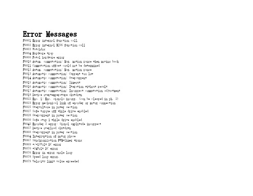
Error MessagesF9001 Error internal function call.F9002 Error internal RTOS function callF9003 WatchdogF9004 Hardware trapF8000 Fatal hardware errorF8010 Autom. commutation: Max. motion range when moving back F8011 Commutation offset could not be determinedF8012 Autom. commutation: Max. motion rangeF8013 Automatic commutation: Current too lowF8014 Automatic commutation: OvercurrentF8015 Automatic commutation: TimeoutF8016 Automatic commutation: Iteration without resultF8017 Automatic commutation: Incorrect commutation adjustment F8018 Device overtemperature shutdownF8022 Enc. 1: Enc. signals incorr. (can be cleared in ph. 2) F8023 Error mechanical link of encoder or motor connectionF8025 Overvoltage in power sectionF8027 Safe torque off while drive enabledF8028 Overcurrent in power sectionF8030 Safe stop 1 while drive enabledF8042 Encoder 2 error: Signal amplitude incorrectF8057 Device overload shutdownF8060 Overcurrent in power sectionF8064 Interruption of motor phaseF8067 Synchronization PWM-Timer wrongF8069 +/-15Volt DC errorF8070 +24Volt DC errorF8076 Error in error angle loopF8078 Speed loop error.F8079 Velocity limit value exceededF8091 Power section defectiveF8100 Error when initializing the parameter handlingF8102 Error when initializing power sectionF8118 Invalid power section/firmware combinationF8120 Invalid control section/firmware combinationF8122 Control section defectiveF8129 Incorrect optional module firmwareF8130 Firmware of option 2 of safety technology defectiveF8133 Error when checking interrupting circuitsF8134 SBS: Fatal errorF8135 SMD: Velocity exceededF8140 Fatal CCD error.F8201 Safety command for basic initialization incorrectF8203 Safety technology configuration parameter invalidF8813 Connection error mains chokeF8830 Power section errorF8838 Overcurrent external braking resistorF7010 Safely-limited increment exceededF7011 Safely-monitored position, exceeded in pos. DirectionF7012 Safely-monitored position, exceeded in neg. DirectionF7013 Safely-limited speed exceededF7020 Safe maximum speed exceededF7021 Safely-limited position exceededF7030 Position window Safe stop 2 exceededF7031 Incorrect direction of motionF7040 Validation error parameterized - effective thresholdF7041 Actual position value validation errorF7042 Validation error of safe operation modeF7043 Error of output stage interlockF7050 Time for stopping process exceeded8.3.15 F7051 Safely-monitored deceleration exceeded (159)8.4 Travel Range Errors (F6xxx) (161)8.4.1 Behavior in the Case of Travel Range Errors (161)8.4.2 F6010 PLC Runtime Error (162)8.4.3 F6024 Maximum braking time exceeded (163)8.4.4 F6028 Position limit value exceeded (overflow) (164)8.4.5 F6029 Positive position limit exceeded (164)8.4.6 F6030 Negative position limit exceeded (165)8.4.7 F6034 Emergency-Stop (166)8.4.8 F6042 Both travel range limit switches activated (167)8.4.9 F6043 Positive travel range limit switch activated (167)8.4.10 F6044 Negative travel range limit switch activated (168)8.4.11 F6140 CCD slave error (emergency halt) (169)8.5 Interface Errors (F4xxx) (169)8.5.1 Behavior in the Case of Interface Errors (169)8.5.2 F4001 Sync telegram failure (170)8.5.3 F4002 RTD telegram failure (171)8.5.4 F4003 Invalid communication phase shutdown (172)8.5.5 F4004 Error during phase progression (172)8.5.6 F4005 Error during phase regression (173)8.5.7 F4006 Phase switching without ready signal (173)8.5.8 F4009 Bus failure (173)8.5.9 F4012 Incorrect I/O length (175)8.5.10 F4016 PLC double real-time channel failure (176)8.5.11 F4017 S-III: Incorrect sequence during phase switch (176)8.5.12 F4034 Emergency-Stop (177)8.5.13 F4140 CCD communication error (178)8.6 Non-Fatal Safety Technology Errors (F3xxx) (178)8.6.1 Behavior in the Case of Non-Fatal Safety Technology Errors (178)8.6.2 F3111 Refer. missing when selecting safety related end pos (179)8.6.3 F3112 Safe reference missing (179)8.6.4 F3115 Brake check time interval exceeded (181)Troubleshooting Guide | Rexroth IndraDrive Electric Drivesand ControlsI Bosch Rexroth AG VII/XXIITable of ContentsPage8.6.5 F3116 Nominal load torque of holding system exceeded (182)8.6.6 F3117 Actual position values validation error (182)8.6.7 F3122 SBS: System error (183)8.6.8 F3123 SBS: Brake check missing (184)8.6.9 F3130 Error when checking input signals (185)8.6.10 F3131 Error when checking acknowledgment signal (185)8.6.11 F3132 Error when checking diagnostic output signal (186)8.6.12 F3133 Error when checking interrupting circuits (187)8.6.13 F3134 Dynamization time interval incorrect (188)8.6.14 F3135 Dynamization pulse width incorrect (189)8.6.15 F3140 Safety parameters validation error (192)8.6.16 F3141 Selection validation error (192)8.6.17 F3142 Activation time of enabling control exceeded (193)8.6.18 F3143 Safety command for clearing errors incorrect (194)8.6.19 F3144 Incorrect safety configuration (195)8.6.20 F3145 Error when unlocking the safety door (196)8.6.21 F3146 System error channel 2 (197)8.6.22 F3147 System error channel 1 (198)8.6.23 F3150 Safety command for system start incorrect (199)8.6.24 F3151 Safety command for system halt incorrect (200)8.6.25 F3152 Incorrect backup of safety technology data (201)8.6.26 F3160 Communication error of safe communication (202)8.7 Non-Fatal Errors (F2xxx) (202)8.7.1 Behavior in the Case of Non-Fatal Errors (202)8.7.2 F2002 Encoder assignment not allowed for synchronization (203)8.7.3 F2003 Motion step skipped (203)8.7.4 F2004 Error in MotionProfile (204)8.7.5 F2005 Cam table invalid (205)8.7.6 F2006 MMC was removed (206)8.7.7 F2007 Switching to non-initialized operation mode (206)8.7.8 F2008 RL The motor type has changed (207)8.7.9 F2009 PL Load parameter default values (208)8.7.10 F2010 Error when initializing digital I/O (-> S-0-0423) (209)8.7.11 F2011 PLC - Error no. 1 (210)8.7.12 F2012 PLC - Error no. 2 (210)8.7.13 F2013 PLC - Error no. 3 (211)8.7.14 F2014 PLC - Error no. 4 (211)8.7.15 F2018 Device overtemperature shutdown (211)8.7.16 F2019 Motor overtemperature shutdown (212)8.7.17 F2021 Motor temperature monitor defective (213)8.7.18 F2022 Device temperature monitor defective (214)8.7.19 F2025 Drive not ready for control (214)8.7.20 F2026 Undervoltage in power section (215)8.7.21 F2027 Excessive oscillation in DC bus (216)8.7.22 F2028 Excessive deviation (216)8.7.23 F2031 Encoder 1 error: Signal amplitude incorrect (217)VIII/XXII Bosch Rexroth AG | Electric Drivesand ControlsRexroth IndraDrive | Troubleshooting GuideTable of ContentsPage8.7.24 F2032 Validation error during commutation fine adjustment (217)8.7.25 F2033 External power supply X10 error (218)8.7.26 F2036 Excessive position feedback difference (219)8.7.27 F2037 Excessive position command difference (220)8.7.28 F2039 Maximum acceleration exceeded (220)8.7.29 F2040 Device overtemperature 2 shutdown (221)8.7.30 F2042 Encoder 2: Encoder signals incorrect (222)8.7.31 F2043 Measuring encoder: Encoder signals incorrect (222)8.7.32 F2044 External power supply X15 error (223)8.7.33 F2048 Low battery voltage (224)8.7.34 F2050 Overflow of target position preset memory (225)8.7.35 F2051 No sequential block in target position preset memory (225)8.7.36 F2053 Incr. encoder emulator: Pulse frequency too high (226)8.7.37 F2054 Incr. encoder emulator: Hardware error (226)8.7.38 F2055 External power supply dig. I/O error (227)8.7.39 F2057 Target position out of travel range (227)8.7.40 F2058 Internal overflow by positioning input (228)8.7.41 F2059 Incorrect command value direction when positioning (229)8.7.42 F2063 Internal overflow master axis generator (230)8.7.43 F2064 Incorrect cmd value direction master axis generator (230)8.7.44 F2067 Synchronization to master communication incorrect (231)8.7.45 F2068 Brake error (231)8.7.46 F2069 Error when releasing the motor holding brake (232)8.7.47 F2074 Actual pos. value 1 outside absolute encoder window (232)8.7.48 F2075 Actual pos. value 2 outside absolute encoder window (233)8.7.49 F2076 Actual pos. value 3 outside absolute encoder window (234)8.7.50 F2077 Current measurement trim wrong (235)8.7.51 F2086 Error supply module (236)8.7.52 F2087 Module group communication error (236)8.7.53 F2100 Incorrect access to command value memory (237)8.7.54 F2101 It was impossible to address MMC (237)8.7.55 F2102 It was impossible to address I2C memory (238)8.7.56 F2103 It was impossible to address EnDat memory (238)8.7.57 F2104 Commutation offset invalid (239)8.7.58 F2105 It was impossible to address Hiperface memory (239)8.7.59 F2110 Error in non-cyclical data communic. of power section (240)8.7.60 F2120 MMC: Defective or missing, replace (240)8.7.61 F2121 MMC: Incorrect data or file, create correctly (241)8.7.62 F2122 MMC: Incorrect IBF file, correct it (241)8.7.63 F2123 Retain data backup impossible (242)8.7.64 F2124 MMC: Saving too slowly, replace (243)8.7.65 F2130 Error comfort control panel (243)8.7.66 F2140 CCD slave error (243)8.7.67 F2150 MLD motion function block error (244)8.7.68 F2174 Loss of motor encoder reference (244)8.7.69 F2175 Loss of optional encoder reference (245)Troubleshooting Guide | Rexroth IndraDrive Electric Drivesand Controls| Bosch Rexroth AG IX/XXIITable of ContentsPage8.7.70 F2176 Loss of measuring encoder reference (246)8.7.71 F2177 Modulo limitation error of motor encoder (246)8.7.72 F2178 Modulo limitation error of optional encoder (247)8.7.73 F2179 Modulo limitation error of measuring encoder (247)8.7.74 F2190 Incorrect Ethernet configuration (248)8.7.75 F2260 Command current limit shutoff (249)8.7.76 F2270 Analog input 1 or 2, wire break (249)8.7.77 F2802 PLL is not synchronized (250)8.7.78 F2814 Undervoltage in mains (250)8.7.79 F2815 Overvoltage in mains (251)8.7.80 F2816 Softstart fault power supply unit (251)8.7.81 F2817 Overvoltage in power section (251)8.7.82 F2818 Phase failure (252)8.7.83 F2819 Mains failure (253)8.7.84 F2820 Braking resistor overload (253)8.7.85 F2821 Error in control of braking resistor (254)8.7.86 F2825 Switch-on threshold braking resistor too low (255)8.7.87 F2833 Ground fault in motor line (255)8.7.88 F2834 Contactor control error (256)8.7.89 F2835 Mains contactor wiring error (256)8.7.90 F2836 DC bus balancing monitor error (257)8.7.91 F2837 Contactor monitoring error (257)8.7.92 F2840 Error supply shutdown (257)8.7.93 F2860 Overcurrent in mains-side power section (258)8.7.94 F2890 Invalid device code (259)8.7.95 F2891 Incorrect interrupt timing (259)8.7.96 F2892 Hardware variant not supported (259)8.8 SERCOS Error Codes / Error Messages of Serial Communication (259)9 Warnings (Exxxx) (263)9.1 Fatal Warnings (E8xxx) (263)9.1.1 Behavior in the Case of Fatal Warnings (263)9.1.2 E8025 Overvoltage in power section (263)9.1.3 E8026 Undervoltage in power section (264)9.1.4 E8027 Safe torque off while drive enabled (265)9.1.5 E8028 Overcurrent in power section (265)9.1.6 E8029 Positive position limit exceeded (266)9.1.7 E8030 Negative position limit exceeded (267)9.1.8 E8034 Emergency-Stop (268)9.1.9 E8040 Torque/force actual value limit active (268)9.1.10 E8041 Current limit active (269)9.1.11 E8042 Both travel range limit switches activated (269)9.1.12 E8043 Positive travel range limit switch activated (270)9.1.13 E8044 Negative travel range limit switch activated (271)9.1.14 E8055 Motor overload, current limit active (271)9.1.15 E8057 Device overload, current limit active (272)X/XXII Bosch Rexroth AG | Electric Drivesand ControlsRexroth IndraDrive | Troubleshooting GuideTable of ContentsPage9.1.16 E8058 Drive system not ready for operation (273)9.1.17 E8260 Torque/force command value limit active (273)9.1.18 E8802 PLL is not synchronized (274)9.1.19 E8814 Undervoltage in mains (275)9.1.20 E8815 Overvoltage in mains (275)9.1.21 E8818 Phase failure (276)9.1.22 E8819 Mains failure (276)9.2 Warnings of Category E4xxx (277)9.2.1 E4001 Double MST failure shutdown (277)9.2.2 E4002 Double MDT failure shutdown (278)9.2.3 E4005 No command value input via master communication (279)9.2.4 E4007 SERCOS III: Consumer connection failed (280)9.2.5 E4008 Invalid addressing command value data container A (280)9.2.6 E4009 Invalid addressing actual value data container A (281)9.2.7 E4010 Slave not scanned or address 0 (281)9.2.8 E4012 Maximum number of CCD slaves exceeded (282)9.2.9 E4013 Incorrect CCD addressing (282)9.2.10 E4014 Incorrect phase switch of CCD slaves (283)9.3 Possible Warnings When Operating Safety Technology (E3xxx) (283)9.3.1 Behavior in Case a Safety Technology Warning Occurs (283)9.3.2 E3100 Error when checking input signals (284)9.3.3 E3101 Error when checking acknowledgment signal (284)9.3.4 E3102 Actual position values validation error (285)9.3.5 E3103 Dynamization failed (285)9.3.6 E3104 Safety parameters validation error (286)9.3.7 E3105 Validation error of safe operation mode (286)9.3.8 E3106 System error safety technology (287)9.3.9 E3107 Safe reference missing (287)9.3.10 E3108 Safely-monitored deceleration exceeded (288)9.3.11 E3110 Time interval of forced dynamization exceeded (289)9.3.12 E3115 Prewarning, end of brake check time interval (289)9.3.13 E3116 Nominal load torque of holding system reached (290)9.4 Non-Fatal Warnings (E2xxx) (290)9.4.1 Behavior in Case a Non-Fatal Warning Occurs (290)9.4.2 E2010 Position control with encoder 2 not possible (291)9.4.3 E2011 PLC - Warning no. 1 (291)9.4.4 E2012 PLC - Warning no. 2 (291)9.4.5 E2013 PLC - Warning no. 3 (292)9.4.6 E2014 PLC - Warning no. 4 (292)9.4.7 E2021 Motor temperature outside of measuring range (292)9.4.8 E2026 Undervoltage in power section (293)9.4.9 E2040 Device overtemperature 2 prewarning (294)9.4.10 E2047 Interpolation velocity = 0 (294)9.4.11 E2048 Interpolation acceleration = 0 (295)9.4.12 E2049 Positioning velocity >= limit value (296)9.4.13 E2050 Device overtemp. Prewarning (297)Troubleshooting Guide | Rexroth IndraDrive Electric Drivesand Controls| Bosch Rexroth AG XI/XXIITable of ContentsPage9.4.14 E2051 Motor overtemp. prewarning (298)9.4.15 E2053 Target position out of travel range (298)9.4.16 E2054 Not homed (300)9.4.17 E2055 Feedrate override S-0-0108 = 0 (300)9.4.18 E2056 Torque limit = 0 (301)9.4.19 E2058 Selected positioning block has not been programmed (302)9.4.20 E2059 Velocity command value limit active (302)9.4.21 E2061 Device overload prewarning (303)9.4.22 E2063 Velocity command value > limit value (304)9.4.23 E2064 Target position out of num. range (304)9.4.24 E2069 Holding brake torque too low (305)9.4.25 E2070 Acceleration limit active (306)9.4.26 E2074 Encoder 1: Encoder signals disturbed (306)9.4.27 E2075 Encoder 2: Encoder signals disturbed (307)9.4.28 E2076 Measuring encoder: Encoder signals disturbed (308)9.4.29 E2077 Absolute encoder monitoring, motor encoder (encoder alarm) (308)9.4.30 E2078 Absolute encoder monitoring, opt. encoder (encoder alarm) (309)9.4.31 E2079 Absolute enc. monitoring, measuring encoder (encoder alarm) (309)9.4.32 E2086 Prewarning supply module overload (310)9.4.33 E2092 Internal synchronization defective (310)9.4.34 E2100 Positioning velocity of master axis generator too high (311)9.4.35 E2101 Acceleration of master axis generator is zero (312)9.4.36 E2140 CCD error at node (312)9.4.37 E2270 Analog input 1 or 2, wire break (312)9.4.38 E2802 HW control of braking resistor (313)9.4.39 E2810 Drive system not ready for operation (314)9.4.40 E2814 Undervoltage in mains (314)9.4.41 E2816 Undervoltage in power section (314)9.4.42 E2818 Phase failure (315)9.4.43 E2819 Mains failure (315)9.4.44 E2820 Braking resistor overload prewarning (316)9.4.45 E2829 Not ready for power on (316)。