NT78BS5DC12V0.8中文资料
uPD780055GCA-xxx-8BT资料

Detaileபைடு நூலகம் function descriptions are provided in the following user’s manuals. Be sure to read them before
64-pin 42/44-pin
Control
µPD78075B µPD78078 µPD78070A
µ PD780058 µPD78058F µPD78054 µPD780065 µPD780078 µPD780034A µPD780024A µPD78014H µPD78018F µPD78083
µPD78005xY(A)) are products of the µPD780058Y Subseries in the 78K/0 Series. These microcontrollers show a reduction in the EMI (Electro Magnetic Interference) noise generated internally
DATA SHEET MOS INTEGRATED CIRCUIT
µPD780053(A), 780054(A), 780055(A), 780056(A), 780058B(A), 780053Y(A), 780054Y(A), 780055Y(A), 780056Y(A), 780058BY(A)
78K/0 Series
Products in mass production
ADC78H90CIMTNOPB;ADC78H90CIMTXNOPB;中文规格书,Datasheet资料

ADC78H90ADC78H90 8-Channel, 500 kSPS, 12-Bit A/D ConverterLiterature Number: SNAS227CADC78H908-Channel,500kSPS,12-Bit A/D ConverterGeneral DescriptionThe ADC78H90is a low-power,eight-channel CMOS 12-bit analog-to-digital converter with a conversion throughput of 500kSPS.The converter is based on a successive-approximation register architecture with an internal track-and-hold circuit.It can be configured to accept up to eight input signals at inputs AIN1through AIN8.The output serial data is straight binary,and is compatible with several standards,such as SPI ™,QSPI ™,MICROW-IRE ™,and many common DSP serial interfaces.The ADC78H90may be operated with independent analog and digital supplies.The analog supply (AV DD )can range from +2.7V to +5.25V,and the digital supply (DV DD )can range from +2.7V to AV DD .Normal power consumption using a +3V or +5V supply is 1.5mW and 8.3mW,respectively.The power-down feature reduces the power consumption to just 0.3µW using a +3V supply,or 0.5µW using a +5V supply.The ADC78H90is packaged in a 16-lead TSSOP package.Operation over the industrial temperature range of −40˚C to +85˚C is guaranteed.Featuresn Eight input channelsn Variable power managementn Independent analog and digital suppliesn SPI ™/QSPI ™/MICROWIRE ™/DSP compatible nPackaged in 16-lead TSSOPKey Specificationsn Conversion Rate 500kSPS n DNL ±1LSB (max)n INL±1LSB (max)nPower Consumption —3V Supply 1.5mW (typ)—5V Supply8.3mW (typ)Applicationsn Automotive Navigation n Portable Systems n Medical Instruments n Mobile CommunicationsnInstrumentation and Control SystemsConnection Diagram20079305Ordering InformationOrder CodeTemperature Range DescriptionADC78H90CIMT −40˚C to +85˚C 16-Lead TSSOP PackageADC78H90CIMTX −40˚C to +85˚C16-Lead TSSOP Package,Tape &ReelADC78H90EVALEvaluation BoardTRI-STATE ®is a trademark of National Semiconductor Corporation.MICROWIRE ™is a trademark of National Semiconductor Corporation.QSPI ™and SPI ™are trademarks of Motorola,Inc.©2005National Semiconductor Corporation 20079307Pin Descriptions and Equivalent CircuitsPin No.SymbolEquivalent CircuitDescriptionANALOG I/O 4-11AIN1to AIN8Analog inputs.These signals can range from 0V to AVDIGITAL I/O16SCLKDigital clock input.The range of frequencies for this in 50kHz to 8MHz,with guaranteed performance at 8M This clock directly controls the conversion and readou processes.15DOUT Digital data output.The output samples are clocked ou pin on falling edges of the SCLK pin.14DIN Digital data input.The ADC78H90’s Control Register i loaded through this pin on rising edges of the SCLK p1CSChip select.On the falling edge of CS,a conversion p begins.Conversions continue as long as CS is held loPOWER SUPPLY2AV DDPositive analog supply pin.This pin should be connec quiet +2.7V to +5.25V source and bypassed to GND w µF tantalum capacitor and a 0.1µF ceramic monolithic capacitor located within 1cm of the power pin.13DV DDPositive digital supply pin.This pin should be connecte +2.7V to AV DD supply,and bypassed to GND with a 0ceramic monolithic capacitor located within 1cm of the pin.3AGND The ground return for the analog supply and signals.12DGNDThe ground return for the digital supply and signals.A D 2please contact the National Semiconductor Sales Office/ Distributors for availability and specifications.Analog Supply Voltage AV DD−0.3V to6.5V Digital Supply Voltage DV DD−0.3V to AV DD+0.3V,max6.5V Voltage on Any Pin to GND−0.3V to AV DD+0.3V Input Current at Any Pin(Note3)±10mA Package Input Current(Note3)±20mA Power Dissipation at T A=25˚C See(Note4) ESD Susceptibility(Note5)Human Body Model Machine Model 2500V 250VSoldering Temperature,Infrared,10seconds(Note6)260˚C Junction Temperature+150˚C Storage Temperature−65˚C to+150˚CAAV DD Supply Voltage+2.7V to+5.25V DV DD Supply Voltage+2.7V to AV DD Digital Input Pins Voltage Range-0.3V to AV DD Clock Frequency50kHz to8MHz Analog Input Voltage0V to AV DDPackage Thermal ResistancePackageθJA16-lead TSSOP on4-layer,2oz.PCB96˚C/WADC78H90Converter Electrical Characteristics(Note8)The following specifications apply for AV DD=DV DD=+2.7V to5.25V,AGND=DGND=0V,f SCLK=8MHz,f SAMPLE=500 KSPS,unless otherwise noted.Boldface limits apply for T A=T MIN to T MAX:all other limits T A=25˚C.Symbol Parameter Conditions TypicalLimits(Note7)UnitsSTATIC CONVERTER CHARACTERISTICSResolution with No Missing Codes12Bits INL Integral Non-Linearity AV DD=+5.0V,DV DD=+3.0V±1LSB(max) DNL Differential Non-Linearity AV DD=+5.0V,DV DD=+3.0V±1LSB(max) V OFF Offset Error AV DD=+5.0V,DV DD=+3.0V±2LSB(max) OEM Offset Error Match AV DD=+5.0V,DV DD=+3.0V±2LSB(max) GE Gain Error AV DD=+5.0V,DV DD=+3.0V±3LSB(max) GEM Gain Error Match AV DD=+5.0V,DV DD=+3.0V±3LSB(max) DYNAMIC CONVERTER CHARACTERISTICSSINAD Signal-to-Noise Plus Distortion Ratio AV DD=+5.0V,DV DD=+3.0V,f IN=40.2kHz,−0.02dBFS7370dB(min)SNR Signal-to-Noise Ratio AV DD=+5.0V,DV DD=+3.0V,f IN=40.2kHz,−0.02dBFS7370.8dB(min)THD Total Harmonic Distortion AV DD=+5.0V,DV DD=+3.0V,f IN=40.2kHz,−0.02dBFS−86−74dB(max)SFDR Spurious-Free Dynamic Range AV DD=+5.0V,DV DD=+3.0V,f IN=40.2kHz,−0.02dBFS8875.6dB(min)ENOB Effective Number of Bits AV DD=+5.0V,DV DD=+3.0V,11.811.3Bits(min)Channel-to-Channel Crosstalk AV DD=+5.0V,DV DD=+3.0V,f IN=40.2kHz-82dBIMD Intermodulation Distortion,SecondOrder TermsAV DD=+5.0V,DV DD=+3.0V,f a=40.161kHz,f b=41.015kHz-93dB Intermodulation Distortion,ThirdOrder TermsAV DD=+5.0V,DV DD=+3.0V,f a=40.161kHz,f b=41.015kHz-90dBFPBW-3dB Full Power Bandwidth AV DD=+5V11MHzAV DD=+3V8MHz 3KSPS,unless otherwise noted.Boldface limits apply for T A =T MIN to T MAX :all other limits T A =25˚C.SymbolParameterConditionsTypicalLimits (Note 7)UANALOG INPUT CHARACTERISTICS V IN Input Range 0to AV DDI DCL DC Leakage Current ±1µAC INAInput CapacitanceTrack Mode 33Hold Mode3DIGITAL INPUT CHARACTERISTICS V IH Input High Voltage DV DD =+4.75Vto +5.25V 2.4V (DV DD =+2.7V to +3.6V 2.1V (V IL Input Low Voltage DV DD =+2.7V to +5.25V 0.8V (I IN Input CurrentV IN =0V or DV DD±0.01±1µA C INDDigital Input Capacitance24pFDIGITAL OUTPUT CHARACTERISTICS V OH Output High Voltage I SOURCE =200µA,DV DD =+2.7V to +5.25V DV DD −0.5V (V OL Output Low VoltageI SINK =200µA0.4V (I OZH ,I OZL TRI-STATE ®Leakage Current ±1µA C OUTTRI-STATE ®Output Capacitance 24pFOutput CodingStraight (Natural)BinaryPOWER SUPPLY CHARACTERISTICS (C L =10pF)AV DD ,DV DDAnalog and Digital Supply VoltagesAV DD ≥DV DD2.7V (5.25V (I A +I DTotal Supply Current,Normal Mode (Operational,CS low)AV DD =DV DD =+4.75V to +5.25V,f SAMPLE =500kSPS,f IN =40kHz 1.65 2.3mA AV DD =DV DD =+2.7V to +3.6V,f SAMPLE =500kSPS,f IN =40kHz 0.5 2.3mATotal Supply Current,Shutdown (CS high)AV DD =DV DD =+4.75V to +5.25V,f SAMPLE =0kSPS200AV DD =DV DD =+2.7V to +3.6V,f SAMPLE =0kSPS200P DPower Consumption,Normal Mode (Operational,CS low)\AV DD =DV DD =+4.75V to +5.25V 8.312mWAV DD =DV DD =+2.7V to +3.6V 1.58.3mWPower Consumption,Shutdown (CS high)AV DD =DV DD =+4.75V to +5.25V 0.5µAV DD =DV DD =+2.7V to +3.6V0.3µAC ELECTRICAL CHARACTERISTICS f SCLK Maximum Clock Frequency 8MHzf SMIN Minimum Clock Frequency 50kf S Maximum Sample Rate 500KSPS t CONV Conversion Time 13SCLKDC SCLK Duty Cycle5040%60%(t ACQTrack/Hold Acquisition Time Full-Scale Step Input3SCLKThroughput TimeAcquisition Time +Conversion Time16SCLKf RATE Throughput Rate 500kSPSt ADAperture Delay4A D 4KSPS,C L=50pF,Boldface limits apply for T A=T MIN to T MAX:all other limits T A=25˚C.Symbol Parameter Conditions TypicalLimits(Note7)Unitst1a Setup Time SCLK High to CSFalling Edge(Note9)10ns(min)t1b Hold time SCLK Low to CS FallingEdge(Note9)10ns(min)t2Delay from CS Until DOUT active30ns(max)t3Data Access Time after SCLKFalling Edge30ns(max)t4Data Setup Time Prior to SCLKRising Edge10ns(min)t5Data Valid SCLK Hold Time10ns(min)t6SCLK High Pulse Width 0.4xt SCLKns(min)t7SCLK Low Pulse Width 0.4xt SCLKns(min)t8CS Rising Edge to DOUTHigh-Impedance20ns(max)Note1:Absolute Maximum Ratings indicate limits beyond which damage to the device may occur.Operating Ratings indicate conditions for which the device is functional,but do not guarantee specific performance limits.For guaranteed specifications and test conditions,see the Electrical Characteristics.The guaranteed specifications apply only for the test conditions listed.Some performance characteristics may degrade when the device is not operated under the listed test conditions.Note2:All voltages are measured with respect to GND=0V,unless otherwise specified.Note3:When the input voltage at any pin exceeds the power supplies(that is,V IN<AGND or V IN>V A or V D),the current at that pin should be limited to10mA.The20mA maximum package input current rating limits the number of pins that can safely exceed the power supplies with an input current of10mA to two.Note4:The absolute maximum junction temperature(T J max)for this device is150˚C.The maximum allowable power dissipation is dictated by T J max,the junction-to-ambient thermal resistance(θJA),and the ambient temperature(T A),and can be calculated using the formula P D MAX=(T J max−T A)/θJA.In the16-pin TSSOP,θJA is96˚C/W,so P D MAX=1,200mW at25˚C and625mW at the maximum operating ambient temperature of85˚C.Note that the power consumption ofthis device under normal operation is a maximum of12mW.The values for maximum power dissipation listed above will be reached only when the ADC78H90is operated in a severe fault condition(e.g.when input or output pins are driven beyond the power supply voltages,or the power supply polarity is reversed).Obviously, such conditions should always be avoided.Note5:Human body model is100pF capacitor discharged through a1.5kΩresistor.Machine model is220pF discharged through ZERO ohmsNote6:See AN450,“Surface Mounting Methods and Their Effect on Product Reliability”,or the section entitled“Surface Mount”found in any post1986National Semiconductor Linear Data Book,for other methods of soldering surface mount devices.Note7:Tested limits are guaranteed to National’s AOQL(Average Outgoing Quality Level).Note8:Data sheet min/max specification limits are guaranteed by design,test,or statistical analysis.Note9:Clock may be in any state(high or low)when CS is asserted,with the restrictions on setup and hold time given by t1a and t1b.520079308Timing Test Circuit20079306ADC78H90Serial Timing Diagram2007FIGURE 1.ADC78H90Operational Timing DiagramA D 620079350SCLK and CS Timing Parameters7voltage.That is,it is time required for the hold capacitor to charge up to the input voltage.APERTURE DELAY is the time between the fourth falling SCLK edge of a conversion and the time when the input signal is acquired or held for conversion.CONVERSION TIME is the time required,after the input voltage is acquired,for the ADC to convert the input voltage to a digital word.CROSSTALK is the coupling of energy from one channel into the other channel,or the amount of signal energy from one analog input that appears at the measured analog input.DIFFERENTIAL NON-LINEARITY (DNL)is the measure of the maximum deviation from the ideal step size of 1LSB.DUTY CYCLE is the ratio of the time that a repetitive digital waveform is high to the total time of one period.The speci-fication here refers to the SCLK.EFFECTIVE NUMBER OF BITS (ENOB,or EFFECTIVE BITS)is another method of specifying Signal-to-Noise and Distortion or SINAD.ENOB is defined as (SINAD -1.76)/6.02and says that the converter is equivalent to a perfect ADC of this (ENOB)number of bits.FULL POWER BANDWIDTH is a measure of the frequency at which the reconstructed output fundamental drops 3dB below its low frequency value for a full scale input.GAIN ERROR is the deviation of the last code transition (111...110)to (111...111)from the ideal (V REF -1.5LSB),after adjusting for offset error.INTEGRAL NON-LINEARITY (INL)is a measure of the deviation of each individual code from a line drawn from negative full scale (1⁄2LSB below the first code transition)through positive full scale (1⁄2LSB above the last code transition).The deviation of any given code from this straight line is measured from the center of that code value.INTERMODULATION DISTORTION (IMD)is the creation of additional spectral components as a result of two sinusoidal frequencies being applied to the ADC input at the same time.It is defined as the ratio of the power in the second and third order intermodulation products to the sum of the power in both of the original frequencies.IMD is usually expressed in dB.not to have any missing codes.OFFSET ERROR is the deviation of the first code tra (000...000)to (000...001)from the ideal (i.e.GND LSB).SIGNAL TO NOISE RATIO (SNR)is the ratio,expres dB,of the rms value of the input signal to the rms value sum of all other spectral components below one-h sampling frequency,not including harmonics or d.c.SIGNAL TO NOISE PLUS DISTORTION (S/N+D or S Is the ratio,expressed in dB,of the rms value of the signal to the rms value of all of the other spectral c nents below half the clock frequency,including harm but excluding d.c.SPURIOUS FREE DYNAMIC RANGE (SFDR)is the ence,expressed in dB,between the rms values of th signal and the peak spurious signal where a spurious is any signal present in the output spectrum that present at the input,excluding d.c.TOTAL HARMONIC DISTORTION (THD)is the rat pressed in dB or dBc,of the rms total of the fir harmonic components at the output to the rms level input signal frequency as seen at the output.THD is lated aswhere A f1is the RMS power of the input frequency output and A f2through A f6are the RMS power in the harmonic frequencies.THROUGHPUT TIME is the minimum time required be the start of two successive conversion.It is the acqu time plus the conversion time.In the case of the ADC7this is 16SCLK periods.A D 8DNL DNL2007934020079341INL INL2007934220079343DNL vs.Supply INL vs.Supply20079321200793209分销商库存信息: NATIONAL-SEMICONDUCTORADC78H90CIMT/NOP B ADC78H90CIMTX/NO PB。
LM7805中文资料

内部结构框图
绝对最大参数值
参数 输入电压(V0=5V~18V)(V0=24V)
热敏电阻接线外壳(Junction cases)(TO-220) 热敏电阻空气接头(Junction-Air) 工作温度范围 存储温度范围
符号 VI VI
RθJC RθJC TOPR TSTG
数值 35 40 5 65 0~+125 -65~+150
4.8 5.0 5.2
V
4.75 5.0 5.25
15W
VI = 7V ~ 20V
电压调整率
Regli TJ=+25 ℃ ne
Vo=7V~25V VI=8V~12V
- 4.0 100 mV - 1.6 50
负载调整率
Regl TJ=+25℃ aod
Io = 5.0mA ~1.5A
-
9 100 mV
Io=250mA
的脉冲测试使用的是负载。
电气特性(MC7806)
(涉及测试电路,0℃< TJ < 125℃, Io= 500mA,VI =11V, CI= 0.33μF,CO= 0.1μF,除非另有说
明)
参数
符号
状态
MC7806
单位
最 Typ 最
小
大
值
值
输出电压
VO TJ=+25℃
5.7 6.0 6.2
V
5.0mA ≤Io≤ 1.0A, PO≤15W,
5
5
5.7 6.0 6.3
VI = 8.0V ~ 21V
电压调整率 Regline TJ=+25℃ VI=8V~25V
- 5 120 mV
VI=9V~13V
MC78M12中文资料

MC78M12中文资料一、产品概述MC78M12是一款性能稳定的正电压稳压器,采用TO220封装,具有输出电流大、纹波抑制比高等特点。
该产品广泛应用于电子设备、工业控制、通信设备等领域,为您的电路提供稳定可靠的电源保障。
二、产品特点1. 输出电压:+12V2. 输出电流:可达1.5A3. 线性调整率:≤0.01%4. 负载调整率:≤0.1%5. 纹波抑制比:≥60dB6. 工作温度范围:40℃至+125℃7. 安全保护:过流保护、过热保护三、应用领域1. 电子产品:如电视、音响、计算机等2. 工业控制:如PLC、变频器、伺服驱动器等3. 通信设备:如交换机、路由器、光端机等4. 电源模块:如各种DCDC模块、ACDC模块等5. 其他需要稳定电压供电的场合四、电气参数1. 输入电压:18V至35V2. 输出电压:+12V3. 输出电流:1.5A(最大)4. 线性调整率:≤0.01%5. 负载调整率:≤0.1%6. 纹波抑制比:≥60dB7. 工作温度范围:40℃至+125℃8. 绝缘电阻:≥100MΩ五、安装与使用注意事项1. 安装前请确认输入电压、输出电压及电流等参数是否符合产品要求。
2. 确保安装过程中,引脚不受到外力损伤,以免影响产品性能。
4. 在使用过程中,请勿超过产品的最大负载电流,以免损坏产品。
5. 请遵循正确的电路设计原则,确保电路稳定可靠。
六、产品封装与尺寸封装类型:TO220尺寸(mm):长10.16 x 宽4.57 x 高18.71引脚中心距离(mm):2.54请确保在电路板设计时,留有足够的空间以保证散热器的安装和空气流通。
七、安全准则1. 在操作前,请确保输入电源已经断开,以防止电击。
2. 避免在潮湿的环境下使用MC78M12,以免引起短路或漏电。
3. 不要将MC78M12暴露在高温或明火中,以免损坏产品或引起火灾。
4. 在安装或维护MC78M12时,请使用适当的绝缘工具,并采取防静电措施。
LM7812详细中文资料
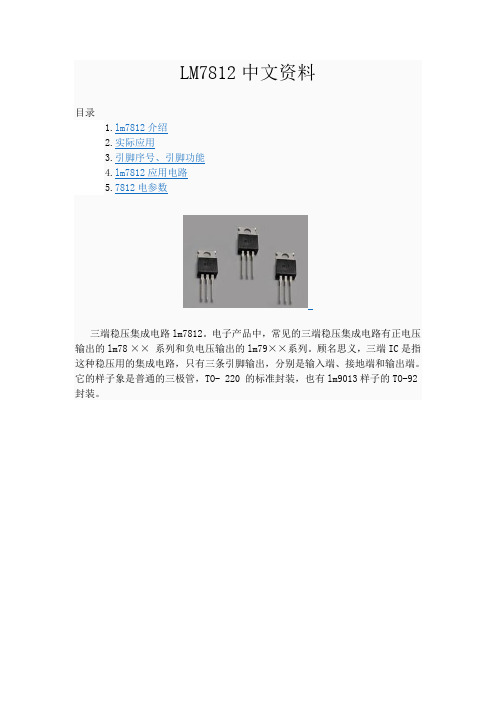
LM7812中文资料目录1.lm7812介绍2.实际应用3.引脚序号、引脚功能4.lm7812应用电路5.7812电参数三端稳压集成电路lm7812。
电子产品中,常见的三端稳压集成电路有正电压输出的lm78 ×× 系列和负电压输出的lm79××系列。
顾名思义,三端IC是指这种稳压用的集成电路,只有三条引脚输出,分别是输入端、接地端和输出端。
它的样子象是普通的三极管,TO- 220 的标准封装,也有lm9013样子的TO-92封装。
1.lm7812介绍用lm78/lm79系列三端稳压IC来组成稳压电源所需的外围元件极少,电路内部还有过流、过热及调整管的保护电路,使用起来可靠、方便,而且价格便宜。
该系列集成稳压IC型号中的lm78或lm79后面的数字代表该三端集成稳压电路的输出电压,如lm7806表示输出电压为正6V,lm7909表示输出电压为负9V。
因为三端固定集成稳压电路的使用方便,电子制作中经常采用。
最大输出电流1.5A,LM78XX系列输出电压分别为5V;6V;8V;9V;10V;12V;15V;18V;24V。
2.实际应用在实际应用中,应在三端集成稳压电路上安装足够大的散热器(当然小功率7812IC内部电路图.的条件下不用)。
当稳压管温度过高时,稳压性能将变差,甚至损坏。
当制作中需要一个能输出1.5A以上电流的稳压电源,通常采用几块三端稳压电路并联起来,使其最大输出电流为N个1.5A,但应用时需注意:并联使用的集成稳压电路应采用同一厂家、同一批号的产品,以保证参数的一致。
另外在输出电流上留有一定的余量,以避免个别集成稳压电路失效时导致其他电路的连锁烧毁。
在lm78 ** 、lm79 ** 系列三端稳压器中最常应用的是TO-220 和TO-202 两种封装。
这两种封装的图形以及引脚序号、引脚功能如附图所示。
图中的引脚号标注方法是按照引脚电位从高到底的顺序标注的。
KA78M05TU,KA78M12TU,KA78M24TU,KA78M15TU,KA78M06TU,KA78M08TU,KA78M08RTM, 规格书,Datasheet 资料

©2011 Fairchild Semiconductor CorporationRev. 1.0.7Features•Output Current up to 0.5A •Output V oltages of 5V•Thermal Overload Protection •Short Circuit Protection•Output Transistor Safe Operating Area (SOA) ProtectionDescriptionThe KA78M05 series of three terminal positive regulators are available in the TO-220/D-PAK package with several fixed output voltages making it useful in a wide range ofapplications.TO-220 (Dual Gauge)D-PAK1. Input2. GND3. Output11GNDGNDInternal Block DiagramOUTPUT3R1R2GND 21INPUT SERIES PASSELEMENTSOAPROTECTIONCURRENT GENERATOR STARTING CIRCUITREFERENCE VOLTAGEERROR AMPLIFIERTHERMAL PROTECTIONKA78M053-Terminal 0.5A Positive Voltage RegulatorKA78M052Absolute Maximum RatingsNote:1. Thermal resistance test boardSize: 76.2mm * 114.3mm * 1.6mm(1S0P)JEDEC standard: JESD51-3, JESD51-72. Assume no ambient airflowElectrical Characteristics (KA78M05/KA78M05R)(Refer to the test circuits, 0 < T J < +125°C, I O =350mA, V I =10V, unless otherwise specified, C I =0.33μF, C O =0.1μF)Note:3. Load and line regulation are specified at constant junction temperature. Change in V o due to heating effects must be takeninto account separately. Pulse testing with low duty is used.ParameterSymbol Value Unit Input Voltage (for V O = 5V)V I 35V Thermal Resistance Junction-Cases (Note1)TO-220 (Tc = +25°C)R θJC 2.5°C/W Thermal Resistance Junction-Air (Note1,2)TO-220 (Ta = +25°C)D-PAK (Ta = +25°C)R θJA 6692°C/W Operating Junction Temperature Range T OPR 0 ~ +150°C Storage Temperature RangeT STG-65 ~ +150°CParameter SymbolConditionsMin.Typ.Max.UnitOutput VoltageV OT J =+25°C4.855.2V I O = 5 to 350mA V I = 7 to 20V 4.755 5.25Line Regulation (Note3)ΔV O I O = 200mA T J =+25°CV I = 7 to 25V --100mV V I = 8 to 25V --50Load Regulation (Note3)ΔV O I O = 5mA to 0.5A, T J = +25°C --100mV I O = 5mA to 200mA, T J =+25°C --50Quiescent Current I Q T J = +25°C - 4.0 6.0mAQuiescent Current ChangeΔI Q I O = 5mA to 350mA --0.5mA I O = 200mA V I = 8 to 25V --0.8Output Voltage Drift ΔV/ΔT I O = 5mAT J = 0 to +125°C --0.5-mV/°COutput Noise Voltage V N f = 10Hz to 100kHz -40-μV/VoRipple Rejection RR f = 120Hz, I O = 300mA V I = 8 to 18V, T J = +25°C -80-dB Dropout Voltage V D T J = +25°C, I O = 500mA -2-V Short Circuit Current I SC T J = +25°C, V I = 35V -300-mA Peak CurrentI PKT J = +25°C-700-mAKA78M053Typical ApplicationsFigure 1.Fixed Output RegulatorFigure 2.Constant Current RegulatorNotes:1.To specify an output voltage, substitute voltage value for "XX"2.Although no output capacitor is needed for stability, it does improve transient response.3.Required if regulator is located an appreciable distance from power Supply filterFigure 3.Circuit for Increasing Output Voltage0.1μFC OC I0.3μFV OV IKA78M051320.1μFC OC I0.33μFI OV IKA78M05132VXXI O R 1I O = R 1 +I OVxx 0.1μFC OC I0.33μFI OV IKA78M05132V XXV OR 1R 2I R1 ≥ 5I OV O = V XX (1+R 2/R 1) +I O R 2KA78M054Figure 4.Adjustable Output Regulator (7 to 30V)Figure 5.0.5 to 10V Regulator0.1μFC OC I0.33μFV OV I KA78M0513210kΩ32476LM7410.1μFC2C10.33μFV OV I KA78M0513210kΩ32476LM741R3R1VXXR4R5910Ω9.1kΩ13V < V I < 25V-7 < -VI< 17V_+V O = VxxR1R4KA78M05 Mechanical DimensionsPackageDimensions in millimetersTO-220 [DUAL GAUGE]5KA78M05Mechanical Dimensions (Continued)PackageDimensions in millimetersD-PAK6KA78M057Ordering InformationProduct NumberPackage Operating TemperatureKA78M05TO-220 (Dual Gauge)0 ~ +125°CKA78M05R D-PAKKA78M0512/30/11 0.0m 001Stock#DS400153© 2011 Fairchild Semiconductor CorporationLIFE SUPPORT POLICYFAIRCHILD’S PRODUCTS ARE NOT AUTHORIZED FOR USE AS CRITICAL COMPONENTS IN LIFE SUPPORT DEVICES OR SYSTEMS WITHOUT THE EXPRESS WRITTEN APPROVAL OF THE PRESIDENT OF FAIRCHILD SEMICONDUCTOR CORPORATION. As used herein:1.Life support devices or systems are devices or systemswhich, (a) are intended for surgical implant into the body, or (b) support or sustain life, and (c) whose failure to perform when properly used in accordance with instructions for use provided in the labeling, can bereasonably expected to result in a significant injury of the user.2. A critical component in any component of a life supportdevice or system whose failure to perform can bereasonably expected to cause the failure of the life support device or system, or to affect its safety or effectiveness.DISCLAIMERFAIRCHILD SEMICONDUCTOR RESERVES THE RIGHT TO MAKE CHANGES WITHOUT FURTHER NOTICE TO ANY PRODUCTS HEREIN TO IMPROVE RELIABILITY, FUNCTION OR DESIGN. FAIRCHILD DOES NOT ASSUME ANYLIABILITY ARISING OUT OF THE APPLICATION OR USE OF ANY PRODUCT OR CIRCUIT DESCRIBED HEREIN; NEITHER DOES IT CONVEY ANY LICENSE UNDER ITS PATENT RIGHTS, NOR THE RIGHTS OF OTHERS.。
SM78L08中文资料
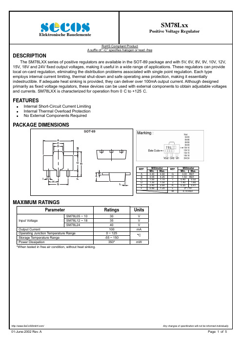
DESCRIPTION
The SM78LXX series of positive regulators are available in the SOT-89 package and with 5V, 6V, 8V, 9V, 10V, 12V, 15V, 18V and 24V fixed output voltages, making it useful in a wide range of applications. These regulators can provide local on-card regulation, eliminating the distribution problems associated with single point regulation. Each type employs internal current limiting, thermal shut-down and safe operating area protection, making it essentially indestructible. If adequate heat sinking is provided, they can deliver over 100mA output current. Although designed primarily as fixed voltage regulators, these devices can be used with external components to obtain adjustable voltages and currents. SM78LXX is characterized for operation from 0°C to +125°C.
DMP78中文说明书1.1

向日葵“无碟王”车载多媒体影音播放器使用说明书(型号:DMP-780)在连接、操作或是调整本产品之前,请仔细阅读下面的介绍。
请保留本手册以备将来参考。
目录1. 功能特点1.1主要特征 (2)2. 主要功能描述2.1面板定义说明 (3)2.2功能菜单说明 (4)3. 基本功能操作3.1状态切换 (5)3.2开机播放 (5)3.3快速向前/向后播放 (5)3.5选择曲目 (5)3.6选择字幕语言 (5)3.7选择音频通道 (5)3.8显示状态 (5)3.9音量控制 (6)3.10高音、低音、左右平衡和响度 (6)3.11播放WMA,MP3等格式文件 (6)4. 收音功能操作4.1选择收音功能 (8)4.2全局搜索自动存储电台 (8)4.3自动搜索电台 (8)4.4手动搜索电台 (8)4.5收听已存储的电台 (8)4.6音量和音效等控制 (8)4.7立体声单声道切换 (8)5. 外接输入操作5.1选择外接输入功能 (9)5.2音量、静音和音效控制 (9)6. 常见问题提示 (10)7. 规格参数 (11)8. 附件 (12)9. 连接图 (12)功能特点1.1主要特征:1 本播放器为标准IN-DASH 尺寸;2 本播放器无机芯,可通过USB接口接U盘,移动硬盘等,另支持SD卡;(可播放CD, MP3,WMA,MPEG-2,MPEG-4等文件格式)3 带调频/调幅收音机,FM频率范围:87.5~108MHz;AM频率范围:522~1620KHz;4 断电记忆功能:当电源突然断掉时,重新开机,机器将从上次断电前那一曲/点播放,而不是从头播放;5 2通道模拟音频输入;6 一路视频输入(可外接倒车摄像头)7 前面板上带AUX IN输入插孔;8 FM可预存30个台,AM可预存12个台;9 2.5寸TFT屏显示;9 阻抗4 Ω时,最大输出4 x 45 W ;10 无机芯设计,有效解决防尘与散热方面的问题;11 全功能面板操作,方便快捷;注意事项:使用时,请在电脑上用FAT32或FAT的格式格式化硬盘/U盘或SD卡,本机暂不支持NTFS格式的文件系统!且硬盘不要分成几个盘区,多分区硬盘可能会导致部分文件无法读到的现象!主要功能描述2.1面板定义说明:1. 上一曲键(在进入多功能菜单时为功能键)2. 播放快退键(在进入多功能菜单时为功能键)3. 播放/暂停键(在进入多功能菜单时为功能键)4. 状态切换键(在同时接上SD卡与USB设备时,按住此键可以在SD卡与USB设备之间切换)5. 下一曲键(在进入多功能菜单时为功能键)6. 播放快进键 (在进入多功能菜单时为功能键)7. 停止键(在进入多功能菜单时为功能键)8. BAND键(在播放状态时为多功能菜单键)在FM/AM状态时为选择波段;在播放USB/SD状态时为多功能菜单选择键,播放时按该键进入数字选曲菜单;再次按该键进入播放设置菜单。
- 1、下载文档前请自行甄别文档内容的完整性,平台不提供额外的编辑、内容补充、找答案等附加服务。
- 2、"仅部分预览"的文档,不可在线预览部分如存在完整性等问题,可反馈申请退款(可完整预览的文档不适用该条件!)。
- 3、如文档侵犯您的权益,请联系客服反馈,我们会尽快为您处理(人工客服工作时间:9:00-18:30)。
Max. 6.6 9.9 13.2 26.4 6.6 9.9 13.2 26.4 60 135 240 960 45 102 180 720
CAUTION: 1.The use of any coil voltage less than the rated coil voltage will compromise the operation of the relay.
2).Inch equivalents are given for general information only.
Reference Data
>àçÇá
Dimensions
Mounting (Bottom views)
Wiring diagram (Bottom views)
0.016 0.020 0.043 0.051 0.055 0.057 0.098 0.138 0.197 0.401 0.848 0.551 0.618
NOTES 1).Dimensions are in millimeter.
-40~85 85% (at 20) 6g
IEC68-2-3Test Ca
Qualification inspection:
Perform the qualification test as specified in the table of IEC255-19-1 and minimum sample size 24.
Ordering Information
NT78 C S 10
1 2 3 4
DC12V 0.6
5 6 4 Contact rating:5A,10A/14VDC;10A/120VAC;5A/250VAC 5 Coil rated Voltage(V):DC:6,9,12,24 6 Coil power consumption:0.6:0.6W;0.8:0.8W
1 Part number:NT78 2 Contact arrangement:A:1A;B:1B;C:1C;U:1U 3 Enclosure:S: Sealed type;NIL: Dust cover
Contact Data
Contact Arrangement Contact Material Contact Rating (resistive) 1A SPSTNO f1B SPSTNC f1C SPDT(B-M)f1U SPSTNODM Ag CdO Ag SnO2 Ag SnO2 In2O3 NO:20A/14VDC 10A/120VAC,5A/250VAC IU:2y10A/14VDC NC:15A/14VDC,10A/120VAC,5A/250VAC Motor load : 1/2HP 125VAC Lamp load : TV-5 280W 1250VA 42VDC 380VAC Max. Switching Current:20A 50m Item 3.12 of IEC255-7 105 Item 3.30 of IEC255-7 107 Item 3.31 of IEC255-7
Max. Switching Power Max. Switching Voltage Contact Resistance or Voltage drop Operation Electrical life Mechanical
Coil Parameter
Coil voltage VDC Pickup voltage VDC(max) (80%of rated voltage ) 4.8 7.2 9.6 19.2 4.8 7.2 9.6 19.2 release voltage VDC(min) (5% of rated voltage) 0.30 0.45 0.60 1.20 0.30 0.45 0.60 1.20 0.8 10 5 0.6 10 5
Safety approvals Safety approval Load
UL NO 20A/14VDC 10A/120VAC NC 10A/14VDC 1/2HP 125VAC TV-5
CCEE 5A/250VAC
Dimensions (Unit: mm)
mm 0.4 0.5 1.1 1.3 1.4 1.45 2.5 3.5 5.0 10.2 12.3 14 15.7
2.Pickup and release voltage are for test purposes only and are not to be used as design criteria.
91
Ambient Temperature Relative Humidity 元器件交易网 Mass
Patent No. 99206529.1
元器件交易网
Features
Small size, light weight. Low coil consumption. PC board mounting. Suitable for household electrical appliance, automation system, electronic equipment, instrument, meter, telecommunication facilities and remote control facilities.
Dash numbers
Coil resistance ±10%
Coil power consumption W
Operate Time ms
Release Time ms
ቤተ መጻሕፍቲ ባይዱ
Rated 006-600 009-600 012-600 024-600 006-800 009-800 012-800 024-800 6 9 12 24 6 9 12 24