EPM3064ATC44-10N中文资料
FPGA可编程逻辑器件芯片EPM3064ATC44-10N中文规格书

Figure2–66.EP2SGX60, EP2SGX90 and EP2SGX130 Device I/O Clock GroupsYou can use the Quartus II software to control whether a clock input pindrives either a global, regional, or dual-regional clock network. TheQuartus II software automatically selects the clocking resources if notspecified.Clock Control BlockEach global clock, regional clock, and PLL external clock output has itsown clock control block. The control block has two functions:■Clock source selection (dynamic selection for global clocks)■Clock power-down (dynamic clock enable or disable)Figure2–69.External PLL Output Clock Control BlocksNotes to Figure2–69:(1)These clock select signals can only be set through a configuration file (.sof or .pof) and cannot be dynamicallycontrolled during user mode operation.(2)The clock control block feeds to a multiplexer within the PLL_OUT pin’s IOE. The PLL_OUT pin is a dual-purposepin. Therefore, this multiplexer selects either an internal signal or the output of the clock control block.For the global clock control block, the clock source selection can becontrolled either statically or dynamically. You have the option ofstatically selecting the clock source by using the Quartus II software to setspecific configuration bits in the configuration file (.sof or .pof) or you cancontrol the selection dynamically by using internal logic to drive themultiplexer select inputs. When selecting statically, the clock source canbe set to any of the inputs to the select multiplexer. When selecting theclock source dynamically, you can either select between two PLL outputs(such as the C0 or C1 outputs from one PLL), between two PLLs (such asthe C0/C1 clock output of one PLL or the C0/C1 c1ock output of the otherPLL), between two clock pins (such as CLK0 or CLK1), or between acombination of clock pins or PLL outputs.For the regional and PLL_OUT clock control block, the clock sourceselection can only be controlled statically using configuration bits. Any ofthe inputs to the clock select multiplexer can be set as the clock source.Operating Conditionsreconfig_clk clockfrequency2.5 -50 2.5 -50 2.5 -50MHzT ransceiverblock minimumpower-downpulse width100--100--100--nsReceiverData rate600-6375600-5000600-4250Mbps Absolute V M A Xfor a receiverpin (1)-- 2.0-- 2.0-- 2.0VAbsolute V M I Nfor a receiverpin-0.4---0.4---0.4--VMaximumpeak-to-peakdifferentialinput voltageV I D (diff p-p)V C M = 0.85V-- 3.3-- 3.3-- 3.3VMinimum peak-to-peak differential input voltage V I D (diff p-p)V C M = 0.85VDC Gain =≥3dB160--160--160--mVV I C M V I C M=0.85V setting850±10%850±10%850±10%mVV I C M=1.2Vsetting (11)1200±10%1200±10%1200±10%mVOn-chip termination resistors 100Ω setting100±15%100±15%100±15%Ω120Ω setting120±15%120±15%120±15%Ω150Ω setting150±15%150±15%150±15%ΩBandwidth at 6.375 Gbps BW = Low-20-------MHz BW = Med-35-------MHz BW = High-45-------MHzTable4–6.Stratix II GX Transceiver Block AC Specification(Part 3 of6)Symbol / Description Conditions-3 Speed CommercialSpeed Grade-4 Speed Commercialand Industrial SpeedGrade-5 Speed CommercialSpeed Grade Unit Min Typ Max Min Typ Max Min Typ Max。
EPM3032ATC44-10中文资料

®Altera Corporation 1MAX 3000AProgrammable Logic Device FamilyJune 2002, ver. 3.0Data Sheet DS-M3000A-3.0Features...■High–performance, low–cost CMOS EEPROM–based programmable logic devices (PLDs) built on a MAX ® architecture (see Table 1)■3.3-V in-system programmability (ISP) through the built–in IEEE Std. 1149.1 Joint Test Action Group (JTAG) interface with advanced pin-locking capability –ISP circuitry compliant with IEEE Std. 1532■Built–in boundary-scan test (BST) circuitry compliant with IEEE Std. 1149.1-1990■Enhanced ISP features:–Enhanced ISP algorithm for faster programming –ISP_Done bit to ensure complete programming –Pull-up resistor on I/O pins during in–system programming ■High–density PLDs ranging from 600 to 10,000 usable gates ■4.5–ns pin–to–pin logic delays with counter frequencies of up to 227.3MHz ■MultiVolt TM I/O interface enabling the device core to run at 3.3 V, while I/O pins are compatible with 5.0–V, 3.3–V, and 2.5–V logic levels ■Pin counts ranging from 44 to 256 in a variety of thin quad flat pack (TQFP), plastic quad flat pack (PQFP), plastic J–lead chip carrier (PLCC), and FineLine BGA TM packages ■Hot–socketing support ■Programmable interconnect array (PIA) continuous routing structurefor fast, predictable performance Table 1.MAX3000A Device Features FeatureEPM3032A EPM3064A EPM3128A EPM3256A EPM3512A Usable gates6001,2502,5005,00010,000Macrocells3264128256512Logic array blocks2481632Maximum user I/Opins346696158208t PD (ns)4.5 4.55.0 5.57.5t SU (ns)2.9 2.83.3 3.9 5.6t CO1 (ns)3.0 3.1 3.4 3.54.7f CNT (MHz)227.3222.2192.3172.4116.3捷多邦,您值得信赖的PCB打样专家!MAX 3000A Programmable Logic Device Family Data Sheet...and More Features ■PCI compatible■Bus–friendly architecture including programmable slew–rate control ■Open–drain output option■Programmable macrocell flipflops with individual clear, preset, clock, and clock enable controls■Programmable power–saving mode for a power reduction of over 50% in each macrocell■Configurable expander product–term distribution, allowing up to32 product terms per macrocell■Programmable security bit for protection of proprietary designs■Enhanced architectural features, including:– 6 or 10 pin– or logic–driven output enable signals–Two global clock signals with optional inversion–Enhanced interconnect resources for improved routability–Programmable output slew–rate control■Software design support and automatic place–and–route provided by Altera’s development systems for Windows–based PCs and Sun SPARCstations, and HP 9000 Series 700/800 workstations■Additional design entry and simulation support provided by EDIF2 0 0 and3 0 0 netlist files, library of parameterized modules (LPM),Verilog HDL, VHDL, and other interfaces to popular EDA tools from third–party manufacturers such as Cadence, Exemplar Logic, Mentor Graphics, OrCAD, Synopsys, Synplicity, and VeriBest■Programming support with the Altera master programming unit (MPU), MasterBlaster TM communications cable, ByteBlasterMV TMparallel port download cable, BitBlaster TM serial download cable as well as programming hardware from third–party manufacturers and any in–circuit tester that supports Jam TM Standard Test andProgramming Language (STAPL) Files (.jam), Jam STAPL Byte-Code Files (.jbc), or Serial Vector Format Files (.svf)General Description MAX3000A devices are low–cost, high–performance devices based on the Altera MAX architecture. Fabricated with advanced CMOS technology, the EEPROM–based MAX3000A devices operate with a 3.3-V supply voltage and provide 600 to 10,000 usable gates, ISP, pin-to-pin delays as fast as 4.5 ns, and counter speeds of up to 227.3MHz. MAX3000A devices in the –4, –5, –6, –7, and –10 speed grades are compatible with the timing requirements of the PCI Special Interest Group (PCI SIG) PCI Local Bus Specification, Revision2.2. See Table2.2Altera CorporationAltera Corporation 3MAX 3000A Programmable Logic Device Family Data Sheet The MAX 3000A architecture supports 100% transistor-to-transistor logic (TTL) emulation and high–density small-scale integration (SSI), medium-scale integration (MSI), and large-scale integration (LSI) logic functions. The MAX 3000A architecture easily integrates multiple devices ranging from PALs, GALs, and 22V10s to MACH and pLSI devices. MAX 3000A devices are available in a wide range of packages, including PLCC, PQFP, and TQFP packages. See Table 3.Note:(1)When the IEEE Std. 1149.1 (JTAG) interface is used for in–system programming or boundary–scan testing, four I/O pins become JTAG pins.MAX 3000A devices use CMOS EEPROM cells to implement logic functions. The user–configurable MAX 3000A architecture accommodates a variety of independent combinatorial and sequential logic functions. The devices can be reprogrammed for quick and efficient iterations during design development and debugging cycles, and can be programmed and erased up to 100 times.Table 2.MAX 3000A Speed Grades Device Speed Grade –4–5–6–7–10EPM3032A v v v EPM3064A vv v EPM3128A v v v EPM3256A v v EPM3512A v v Table 3.MAX 3000A Maximum User I/O Pins Note (1)Device 44–Pin PLCC 44–Pin TQFP 100–Pin TQFP 144–Pin TQFP 208–Pin PQFP 256-Pin FineLine BGA EPM3032A 3434EPM3064A 343466EPM3128A 8096EPM3256A 116158EPM3512A 172208MAX 3000A Programmable Logic Device Family Data SheetMAX3000A devices contain 32 to 512 macrocells, combined into groupsof 16 macrocells called logic array blocks (LABs). Each macrocell has aprogrammable–AND/fixed–OR array and a configurable register withindependently programmable clock, clock enable, clear, and presetfunctions. To build complex logic functions, each macrocell can besupplemented with shareable expander and high–speed parallelexpander product terms to provide up to 32 product terms per macrocell.MAX3000A devices provide programmable speed/power optimization.Speed–critical portions of a design can run at high speed/full power,while the remaining portions run at reduced speed/low power. Thisspeed/power optimization feature enables the designer to configure oneor more macrocells to operate at 50% or lower power while adding only anominal timing delay. MAX3000A devices also provide an option thatreduces the slew rate of the output buffers, minimizing noise transientswhen non–speed–critical signals are switching. The output drivers of allMAX3000A devices can be set for 2.5V or 3.3V, and all input pins are2.5–V,3.3–V, and 5.0-V tolerant, allowing MAX3000A devices to be usedin mixed–voltage systems.MAX3000A devices are supported by Altera development systems,which are integrated packages that offer schematic, text—includingVHDL, Verilog HDL, and the Altera Hardware Description Language(AHDL)—and waveform design entry, compilation and logic synthesis,simulation and timing analysis, and device programming. The softwareprovides EDIF 2 0 0 and 3 0 0, LPM, VHDL, Verilog HDL, and otherinterfaces for additional design entry and simulation support from otherindustry–standard PC– and UNIX–workstation–based EDA tools. Thesoftware runs on Windows–based PCs, as well as Sun SPARCstation, andHP 9000 Series 700/800 workstations.f For more information on development tools, see the MAX+PLUS IIProgrammable Logic Development System & Software Data Sheet andtheQuartus Programmable Logic Development System & Software Data Sheet.Functional Description The MAX3000A architecture includes the following elements:■Logic array blocks (LABs)■Macrocells■Expander product terms (shareable and parallel)■Programmable interconnect array (PIA)■I/O control blocksThe MAX3000A architecture includes four dedicated inputs that can be used as general–purpose inputs or as high–speed, global control signals (clock, clear, and two output enable signals) for each macrocell and I/O pin. Figure1 shows the architecture of MAX3000A devices.4Altera CorporationMAX 3000A Programmable Logic Device Family Data Sheet Figure 1. MAX3000A Device Block DiagramNote:(1)EPM3032A, EPM3064A, EPM3128A, and EPM3256A devices have six output enables. EPM3512A devices have10output enables.Logic Array BlocksThe MAX3000A device architecture is based on the linking ofhigh–performance LABs. LABs consist of 16–macrocell arrays, as shownin Figure1. Multiple LABs are linked together via the PIA, a global busthat is fed by all dedicated input pins, I/O pins, and macrocells.Each LAB is fed by the following signals:■36 signals from the PIA that are used for general logic inputs■Global controls that are used for secondary register functionsAltera Corporation 5MAX 3000A Programmable Logic Device Family Data SheetMacrocellsMAX3000A macrocells can be individually configured for eithersequential or combinatorial logic operation. Macrocells consist of threefunctional blocks: logic array, product–term select matrix, andprogrammable register. Figure2 shows a MAX3000A macrocell.Figure 2. MAX3000A MacrocellQCLRNTo PIACombinatorial logic is implemented in the logic array, which providesfive product terms per macrocell. The product–term select matrixallocates these product terms for use as either primary logic inputs (to theOR and XOR gates) to implement combinatorial functions, or as secondaryinputs to the macrocell’s register preset, clock, and clock enable controlfunctions.Two kinds of expander product terms (“expanders”) are available tosupplement macrocell logic resources:■Shareable expanders, which are inverted product terms that are fedback into the logic array■Parallel expanders, which are product terms borrowed from adjacentmacrocellsThe Altera development system automatically optimizes product–termallocation according to the logic requirements of the design.6Altera CorporationMAX 3000A Programmable Logic Device Family Data SheetFor registered functions, each macrocell flipflop can be individuallyprogrammed to implement D, T, JK, or SR operation with programmableclock control. The flipflop can be bypassed for combinatorial operation.During design entry, the designer specifies the desired flipflop type; theAltera development system software then selects the most efficientflipflop operation for each registered function to optimize resourceutilization.Each programmable register can be clocked in three different modes:■Global clock signal mode, which achieves the fastest clock–to–outputperformance.■Global clock signal enabled by an active–high clock enable. A clockenable is generated by a product term. This mode provides an enableon each flipflop while still achieving the fast clock–to–outputperformance of the global clock.■Array clock implemented with a product term. In this mode, theflipflop can be clocked by signals from buried macrocells or I/O pins.Two global clock signals are available in MAX3000A devices. As shownin Figure1, these global clock signals can be the true or the complement ofeither of the two global clock pins, GCLK1 or GCLK2.Each register also supports asynchronous preset and clear functions. Asshown in Figure2, the product–term select matrix allocates product termsto control these operations. Although the product–term–driven presetand clear from the register are active high, active–low control can beobtained by inverting the signal within the logic array. In addition, eachregister clear function can be individually driven by the active–lowdedicated global clear pin (GCLRn).Expander Product TermsAlthough most logic functions can be implemented with the five productterms available in each macrocell, highly complex logic functions requireadditional product terms. Another macrocell can be used to supply therequired logic resources. However, the MAX3000A architecture alsooffers both shareable and parallel expander product terms (“expanders”)that provide additional product terms directly to any macrocell in thesame LAB. These expanders help ensure that logic is synthesized with thefewest possible logic resources to obtain the fastest possible speed. Altera Corporation 78Altera Corporation MAX 3000A Programmable Logic Device Family Data SheetShareable Expanders Each LAB has 16 shareable expanders that can be viewed as a pool of uncommitted single product terms (one from each macrocell) with inverted outputs that feed back into the logic array. Each shareable expander can be used and shared by any or all macrocells in the LAB to build complex logic functions. Shareable expanders incur a small delay (t SEXP ). Figure 3 shows how shareable expanders can feed multiple macrocells.Figure 3. MAX 3000A Shareable Expanders Shareable expanders can be shared by any or all macrocells in an LAB.Parallel Expanders Parallel expanders are unused product terms that can be allocated to a neighboring macrocell to implement fast, complex logic functions. Parallel expanders allow up to 20 product terms to directly feed the macrocell OR logic, with five product terms provided by the macrocell and 15 parallel expanders provided by neighboring macrocells in the LAB. MacrocellProduct-Term Logic Product-Term Select Matrix Macrocell Product-Term Logic 36 Signals from PIA 16 Shared ExpandersMAX 3000A Programmable Logic Device Family Data SheetThe Altera development system compiler can automatically allocate up tothree sets of up to five parallel expanders to the macrocells that requireadditional product terms. Each set of five parallel expanders incurs asmall, incremental timing delay (t PEXP). For example, if a macrocellrequires 14product terms, the compiler uses the five dedicated productterms within the macrocell and allocates two sets of parallel expanders;the first set includes five product terms, and the second set includes fourproduct terms, increasing the total delay by 2 ×t PEXP.Two groups of eight macrocells within each LAB (e.g., macrocells 1through 8 and 9through 16) form two chains to lend or borrow parallelexpanders. A macrocell borrows parallel expanders from lower–numbered macrocells. For example, macrocell 8 can borrow parallelexpanders from macrocell 7, from macrocells 7 and 6, or from macrocells7, 6, and 5. Within each group of eight, the lowest–numbered macrocellcan only lend parallel expanders and the highest–numbered macrocell canonly borrow them. Figure4 shows how parallel expanders can beborrowed from a neighboring macrocell.Figure 4. MAX3000A Parallel ExpandersUnused product terms in a macrocell can be allocated to a neighboring macrocell.Altera Corporation 9MAX 3000A Programmable Logic Device Family Data SheetProgrammable Interconnect ArrayLogic is routed between LABs on the PIA. This global bus is aprogrammable path that connects any signal source to any destination onthe device. All MAX3000A dedicated inputs, I/O pins, and macrocelloutputs feed the PIA, which makes the signals available throughout theentire device. Only the signals required by each LAB are actually routedfrom the PIA into the LAB. Figure5 shows how the PIA signals are routedinto the LAB. An EEPROM cell controls one input to a two-input AND gate,which selects a PIA signal to drive into the LAB.Figure 5. MAX3000A PIA RoutingWhile the routing delays of channel–based routing schemes in masked orFPGAs are cumulative, variable, and path–dependent, the MAX3000APIA has a predictable delay. The PIA makes a design’s timingperformance easy to predict.I/O Control BlocksThe I/O control block allows each I/O pin to be individually configuredfor input, output, or bidirectional operation. All I/O pins have a tri–statebuffer that is individually controlled by one of the global output enablesignals or directly connected to ground or V CC. Figure6 shows the I/Ocontrol block for MAX3000A devices. The I/O control block has 6 or10global output enable signals that are driven by the true or complementof two output enable signals, a subset of the I/O pins, or a subset of theI/O macrocells.10Altera CorporationMAX 3000A Programmable Logic Device Family Data Sheet Figure 6. I/O Control Block of MAX3000A DevicesNote:(1)EPM3032A, EPM3064A, EPM3128A, and EPM3256A devices have six output enables. EPM3512A devices have10output enables.When the tri–state buffer control is connected to ground, the output istri-stated (high impedance), and the I/O pin can be used as a dedicatedinput. When the tri–state buffer control is connected to V CC, the output isenabled.The MAX3000A architecture provides dual I/O feedback, in whichmacrocell and pin feedbacks are independent. When an I/O pin isconfigured as an input, the associated macrocell can be used for buriedlogic.Altera Corporation 1112Altera Corporation MAX 3000A Programmable Logic Device Family Data SheetIn–SystemProgramma-bilityMAX 3000A devices can be programmed in–system via an industry–standard four–pin IEEE Std. 1149.1-1990 (JTAG) interface. In-system programmability (ISP) offers quick, efficient iterations during design development and debugging cycles. The MAX 3000A architecture internally generates the high programming voltages required to program its EEPROM cells, allowing in–system programming with only a single 3.3–V power supply. During in–system programming, the I/O pins are tri–stated and weakly pulled–up to eliminate board conflicts. The pull–up value is nominally 50 k Ω.MAX 3000A devices have an enhanced ISP algorithm for faster programming. These devices also offer an ISP_Done bit that ensures safe operation when in–system programming is interrupted. This ISP_Done bit, which is the last bit programmed, prevents all I/O pins from driving until the bit is programmed.ISP simplifies the manufacturing flow by allowing devices to be mounted on a printed circuit board (PCB) with standard pick–and–place equipment before they are programmed. MAX 3000A devices can be programmed by downloading the information via in–circuit testers, embedded processors, the MasterBlaster communications cable, the ByteBlasterMV parallel port download cable, and the BitBlaster serial download cable. Programming the devices after they are placed on the board eliminates lead damage on high–pin–count packages (e.g., QFP packages) due to device handling. MAX 3000A devices can be reprogrammed after a system has already shipped to the field. For example, product upgrades can be performed in the field via software or modem. The Jam STAPL programming and test language can be used to program MAX 3000A devices with in–circuit testers, PCs, or embedded processors.fFor more information on using the Jam STAPL programming and test language, see Application Note 88 (Using the Jam Language for ISP & ICR via an Embedded Processor), Application Note 122 (Using Jam STAPL for ISP & ICR via an Embedded Processor) and AN 111 (Embedded Programming Using the 8051 and Jam Byte-Code).The ISP circuitry in MAX 3000A devices is compliant with the IEEE Std. 1532 specification. The IEEE Std. 1532 is a standard developed to allow concurrent ISP between multiple PLD vendors.Programmingwith ExternalHardwareMAX 3000A devices can be programmed on Windows–based PCs with an Altera Logic Programmer card, MPU, and the appropriate device adapter. The MPU performs continuity checking to ensure adequate electrical contact between the adapter and the device. fFor more information, see the Altera Programming Hardware Data Sheet.Altera Corporation 13MAX 3000A Programmable Logic Device Family Data SheetThe Altera software can use text– or waveform–format test vectors createdwith the Altera Text Editor or Waveform Editor to test the programmeddevice. For added design verification, designers can perform functionaltesting to compare the functional device behavior with the results ofsimulation.Data I/O, BP Microsystems, and other programming hardwaremanufacturers also provide programming support for Altera devices.fFor more information, see Programming Hardware Manufacturers .IEEE Std.1149.1 (JTAG)Boundary–ScanSupport MAX 3000A devices include the JTAG BST circuitry defined by IEEE Std.1149.1–1990. Table 4 describes the JTAG instructions supported by MAX 3000A devices. The pin-out tables found on the Altera web site ( ) or the Altera Digital Library show the location of the JTAG control pins for each device. If the JTAG interface is notrequired, the JTAG pins are available as user I/O pins.The instruction register length of MAX 3000A devices is 10 bits. TheIDCODE and USERCODE register length is 32 bits. Tables 5 and 6 showthe boundary–scan register length and device IDCODE information forMAX 3000A devices.Table 4.MAX 3000A JTAG InstructionsJTAG InstructionDescription SAMPLE/PRELOADAllows a snapshot of signals at the device pins to be captured and examined during normal device operation, and permits an initial data pattern output at the device pins EXTESTAllows the external circuitry and board–level interconnections to be tested by forcing a test pattern at the output pins and capturing test results at the input pins BYPASS Places the 1–bit bypass register between the TDI and TDO pins, which allows the BSTdata to pass synchronously through a selected device to adjacent devices during normaldevice operationIDCODE Selects the IDCODE register and places it between the TDI and TDO pins, allowing theIDCODE to be serially shifted out of TDOUSERCODE Selects the 32–bit USERCODE register and places it between the TDI and TDO pins,allowing the USERCODE value to be shifted out of TDOISP InstructionsThese instructions are used when programming MAX 3000A devices via the JTAG portswith the MasterBlaster, ByteBlasterMV, or BitBlaster cable, or when using a Jam STAPLfile, JBC file, or SVF file via an embedded processor or test equipment14Altera Corporation MAX 3000A Programmable Logic Device Family Data SheetNotes:(1)The most significant bit (MSB) is on the left.(2)The least significant bit (LSB) for all JTAG IDCODEs is 1.fSee Application Note 39 (IEEE 1149.1 (JTAG) Boundary–Scan Testing in Altera Devices) for more information on JTAG BST.Table 5.MAX 3000A Boundary–Scan Register Length Device Boundary–Scan Register Length EPM3032A 96EPM3064A 192EPM3128A 288EPM3256A 480EPM3512A 624Table 6.32–Bit MAX 3000A Device IDCODE Value Note (1)Device IDCODE (32 bits)Version (4 Bits)Part Number (16 Bits) Manufacturer’s Identity (11 Bits) 1 (1 Bit) (2)EPM3032A 00010111 0000 0011 0010000011011101EPM3064A 00010111 0000 0110 0100000011011101EPM3128A 00010111 0001 0010 1000000011011101EPM3256A 00010111 0010 0101 0110000011011101EPM3512A 00010111 0101 0001 0010000011011101MAX 3000A Programmable Logic Device Family Data SheetFigure7 shows the timing information for the JTAG signals.Figure 7. MAX3000A JTAG WaveformsTable7 shows the JTAG timing parameters and values for MAX3000Adevices.Table 7.JTAG Timing Parameters & Values for MAX3000A DevicesSymbol Parameter Min Max Unitt JCP TCK clock period 100nst JCH TCK clock high time 50nst JCL TCK clock low time 50nst JPSU JTAG port setup time 20nst JPH JTAG port hold time 45nst JPCO JTAG port clock to output25nst JPZX JTAG port high impedance to valid output25nst JPXZ JTAG port valid output to high impedance25nst JSSU Capture register setup time20nst JSH Capture register hold time45nst JSCO Update register clock to output25nst JSZX Update register high impedance to valid output25nst JSXZ Update register valid output to high impedance25ns Altera Corporation 15MAX 3000A Programmable Logic Device Family Data SheetProgrammable Speed/Power Control MAX3000A devices offer a power–saving mode that supports low-power operation across user–defined signal paths or the entire device. This feature allows total power dissipation to be reduced by 50% or more because most logic applications require only a small fraction of all gates to operate at maximum frequency.The designer can program each individual macrocell in a MAX3000A device for either high–speed or low–power operation. As a result, speed-critical paths in the design can run at high speed, while the remaining paths can operate at reduced power. Macrocells that run at low power incur a nominal timing delay adder (t LPA) for the t LAD, t LAC, t IC, t ACL, t EN, t CPPW and t SEXP parameters.Output Configuration MAX3000A device outputs can be programmed to meet a variety of system–level requirements.MultiVolt I/O InterfaceThe MAX3000A device architecture supports the MultiVolt I/O interface feature, which allows MAX3000A devices to connect to systems with differing supply voltages. MAX3000A devices in all packages can be set for 2.5–V, 3.3–V, or 5.0–V I/O pin operation. These devices have one set of V CC pins for internal operation and input buffers (VCCINT), and another set for I/O output drivers (VCCIO).The VCCIO pins can be connected to either a 3.3–V or 2.5–V power supply, depending on the output requirements. When the VCCIO pins are connected to a 2.5–V power supply, the output levels are compatible with 2.5–V systems. When the VCCIO pins are connected to a 3.3–V power supply, the output high is at 3.3V and is therefore compatible with 3.3-V or 5.0–V systems. Devices operating with V CCIO levels lower than 3.0V incur a nominally greater timing delay of t OD2 instead of t OD1. Inputs can always be driven by 2.5–V, 3.3–V, or 5.0–V signals.Table8 summarizes the MAX3000A MultiVolt I/O support.Note:(1)When V CCIO is 3.3 V, a MAX 3000A device can drive a 2.5–V device that has 3.3–Vtolerant inputs.Table 8.MAX3000A MultiVolt I/O SupportV CCIO Voltage Input Signal (V)Output Signal (V)2.53.3 5.0 2.5 3.3 5.02.5v v v v3.3v v v v v v16Altera CorporationMAX 3000A Programmable Logic Device Family Data SheetOpen–Drain Output OptionMAX3000A devices provide an optional open–drain (equivalent toopen-collector) output for each I/O pin. This open–drain output enablesthe device to provide system–level control signals (e.g., interrupt andwrite enable signals) that can be asserted by any of several devices. It canalso provide an additional wired–OR plane.Open-drain output pins on MAX3000A devices (with a pull-up resistor tothe 5.0-V supply) can drive 5.0-V CMOS input pins that require a high V IH.When the open-drain pin is active, it will drive low. When the pin isinactive, the resistor will pull up the trace to 5.0V, thereby meeting CMOSrequirements. The open-drain pin will only drive low or tri-state; it willnever drive high. The rise time is dependent on the value of the pull-upresistor and load impedance. The I OL current specification should beconsidered when selecting a pull-up resistorSlew–Rate ControlThe output buffer for each MAX3000A I/O pin has an adjustable outputslew rate that can be configured for low–noise or high–speedperformance. A faster slew rate provides high–speed transitions forhigh-performance systems. However, these fast transitions may introducenoise transients into the system. A slow slew rate reduces system noise,but adds a nominal delay of 4 to 5 ns. When the configuration cell isturned off, the slew rate is set for low–noise performance. Each I/O pinhas an individual EEPROM bit that controls the slew rate, allowingdesigners to specify the slew rate on a pin–by–pin basis. The slew ratecontrol affects both the rising and falling edges of the output signal. Design Security All MAX3000A devices contain a programmable security bit that controlsaccess to the data programmed into the device. When this bit isprogrammed, a design implemented in the device cannot be copied orretrieved. This feature provides a high level of design security becauseprogrammed data within EEPROM cells is invisible. The security bit thatcontrols this function, as well as all other programmed data, is reset onlywhen the device is reprogrammed.Generic Testing MAX3000A devices are fully tested. Complete testing of eachprogrammable EEPROM bit and all internal logic elements ensures 100%programming yield. AC test measurements are taken under conditionsequivalent to those shown in Figure8. Test patterns can be used and thenerased during early stages of the production flow.Altera Corporation 17。
EPM7064STC44-10中文资料(Altera)中文数据手册「EasyDatasheet - 矽搜」

MAX 7000器件采用CMOS EEPROM单元实现逻辑功能.用户可 配置MAX 7000架构收容各种独立组合和时序逻辑功能.该设备可以在 设计开发和调试周期被重新编程为快速和有效迭代,并且可以编程和擦 除高达100倍.
5
v v
-7 v v v v v v v v v v
-10P
v v
-10 v v v v v v v v v v
-12P
-12 v v v v v
-15 v v v v v v v v v v v
-15T v
-20
v v v v
v v v
v v
3
芯片中文手册,看全文,戳
MAX 7000可编程逻辑器件系列数据手册
52 52
68 68 64 68 68 64 64
68 68 76 84 84 84 100 84 (2) 100 104 84 (2) 104 124 124 132 (2)
124 164 164 (2) 164 164
(1) (2)
当MAX 7000S设备JTAG接口用于任何边界扫描测试或ISP,四个I / O引脚成为JTAG引脚. 提交设计到该设备包之前执行完整热分析.欲了解更多信息,请参阅 the Altera器件数据手册操作要求.
EPM7192E
3,750 192 12 124 12 7 3 6 90.9
EPM7256E
5,000 256 16 164 12 7 3 6 90.9
gates
宏单元 逻辑阵列 块 极大 用户I / O引脚
tPD (ns) tSU (ns) tFSU (ns) tCO1 (ns) fCNT (MHz)
f
有关在系统可编程3.3-V MAX 7000A或2.5-V信息 MAX 7000B设备,看 MAX 7000A可编程逻辑器件系列 或者 MAX 7000B可编程逻辑器件系列数据 数据表 表.
EL3064

Run LEDGNDInput 3EL3064 | 4-channel analog input terminal 0…10 V, single-ended, 12 bitT he EL3064 analog input terminal processes signals in the range between 0 and 10 V. The voltage is digitised with a resolution of 12 bits and is transmitted (electrically isolated) to the higher-level automation device. The EL3064 EtherCAT Terminal features 2-wire conductors for the four single-ended inputs with a common internal ground potential. The power contacts are connected through. The signal state of the EtherCAT Terminal is indicated by light emitting diodes.EL3064 | ES3064Number of inputs4 (single-ended)Power supplyvia the E-bus Technologysingle-ended Signal voltage0…10 V Distributed clocks–Internal resistance> 130 k ΩInput filter limit frequency1 kHz Conversion time0.625 ms default setting, configurable Resolution12 bit (16 bit presentation, incl. sign)Measuring error< ±0.3 % (relative to full scale value)Electrical isolation500 V (E-bus/signal voltage)Current consumption power contacts–Current consumption E-bustyp. 130 mA Dielectric strengthmax. 30 V Bit width in the process imageinputs: 16 byte Special featuresactivatable FIR/IIR filters, limit value monitoring Weightapprox. 60 g Operating/storage temperature-25…+60 °C/-40…+85 °C Relative humidity95 %, no condensation Vibration/shock resistanceconforms to EN 60068-2-6/EN 60068-2-27EMC immunity/emissionconforms to EN 61000-6-2/EN 61000-6-4Protect. class/installation pos.IP 20/variable Pluggable wiringfor all ESxxxx terminals Approvals CE, UL, ExEL3064Run LED Run LED Run LEDPower contact +24 V Power contact 0 VInput 1GNDInput 2GND Input 4GND Top view Contact assemblyBECKHOFF New Automation Technology We reserve the right to make technical changes.。
科迈特电子狗说明书
科迈特电子狗说明书T306型电子狗使用说明书T306型电子狗针对目前市场上同类产品的缺点进行彻底改进的低价格高性能报警器。
采用双元红外传感器结合先进的单片机数字信号技术,具有误报率低、可靠性高、性价比高、外型美观大方等特点。
适合家庭、办公室、楼梯口和沿街店面等场所防盗报警使用。
功能特点:遥控器代码学习及记忆。
彻底解决遥控器丢失没有地方配制给用户带来的不便;可以增加其它无线发射频率为315MHZ探头或门磁报警;声音大能有效吓阻非法入侵者报警时可输出开关信号联动其它报警设备(选配)。
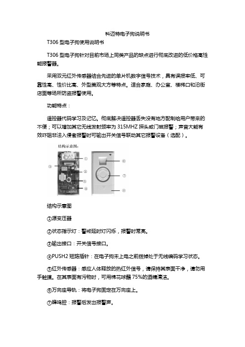
结构示意图①源变压器②状态指示灯:警戒延时灯闪烁,报警时常亮。
③输出接口:开关信号接口。
④PUSH2短路插针:在电子狗未上电之前拨掉处于无线编码学习状态。
⑤红外传感器:感应人体释放的热红外信号,请保持其表面干净,请勿用手触摸。
在其表面有污物时,可用棉花球蘸75%的酒精清洁。
⑥万向座导轨:将电子狗固定在万向座上。
⑦蜂鸣腔:报警后发出报警声。
⑧电池盒:将电池盖打开,安装电池盒内部的标识将9V叠层电池装入。
安装工艺要求:由于电子狗在人体相对于镜片横向运动时红外探测灵敏度最高,而纵向运动灵敏度较差,所以安装时应注意探测器和水平面的夹角和高度,这对防护区域有很大的影响。
安装高度与角度如下图所示。
安装使应避免电子狗靠近冷热源,如冷热出风口、空调出风口、电暖器、冷气机等,避免直对门窗:一电子狗对所防护的范围应可直视,不能有障碍物;电子狗应与墙面成10-30度的夹角,此时探测距离最远,实际安装时根据情况调整安装角度。
将万向座固定在探测器安装在欲安装的位置,安装高度为2米(如下图所示),将探测器固定在万向座上。
参照探测器覆盖区域图,调整万向支架以达到最佳的探测效果。
插上探测器电源插头,探测器上电工作。
使用方法:1、插上电后本机发出一声“嘀”提示声,指示灯闪烁。
如果不进行任何操作,30秒后自动进入“布防”状态。
2、遥控器布撤防和紧急报警①布防:按遥控器上的键,本机两声“嘀,嘀”提示音,本机立即处于布防延时状态,并且指示闪烁,30秒后“嘀,嘀”两声提示音,指示灯息灭后此时本机进入布防状态。
altera产品分析

例如EPM3032ATC44-10N 一片价格大概在 1.4$但是EPM3032ATC44-4N就需要大概2.4$
EPM3064ATC44-10N价格就需要2.5$ EPM3064ATC100-10N价格就要到3.1$。 总结下就是速度越快价格越贵 宏单元越多价格越高。 封装的引脚越多价格也越高。 这个系列最便宜的大概1.4$最高
MAX7000系列 料号举例说明
EPM7128SQC160-15F EPM7 代表是MAX7000系列产品 128 代表有128个宏单元 S 是7000S系列,5V供电的产品 QC160 代表它的封装是PQFP 160条引脚。 15 代表他的芯片速度是15NM
MAX7000系列产品分类比较多。因为不同 电压的算一个分类。我们例举一些产品类 别
MAXII系列和以上讲的3个系列都有些不区 别。前面说的CPLD功能强不强是由它的宏 单元决定的。但是在MAXII系列来说它是结 合了CPLD和FPGA的新产品。它的基本结构 是逻辑单元(FPGA性能指标之一)。
料号举例分析
EPM240T100C5N EPM 代表是MAXII系列 240代表逻辑单元数 T100代表封装和引脚TQFP100条引脚 5N代表是4.7NM的速度
EPM3512AFC256-10就要大概到54$
MAX7000对比MAX3000来说呢。可以当做 MAX3000系列的升级版本。完善了产品线, 对于低端的各种需求都可以更好的满足。
对于MAX7000来说又分为3个系列就是 MAX7000S(5V)、MAX7000AE(3.3V)以及 MAX7000B(2.5V)。目前应用多的就是 MAX7000AE了。
Altera(阿尔特拉)是一家技术势力很强的公 司。是在CPLD和FPGA有着一定的技术领先 的公司。它主要的产品和优势产品就是在
CPLD拉电流及灌电流

© October 2008Altera Corporation Implementing LED Drivers in MAX and MAX II DevicesAN-286-2.3© October 2008Implementing LED Drivers in MAXand MAX II DevicesIntroductionDiscrete LED driver chips are common on many system boards. Altera ®MAX ®II,MAX 7000B, MAX 7000A, MAX 3000A, and MAX 7000S devices offer unique capabilities that allow you to integrate single or multiple LED driver chips into a single device. This application note explains how to implement LED drivers in MAX and MAX II devices.Commercial LED Driver ChipsMany LEDs, such as the seven-segment display, are common-anode LEDs. The LEDs anode connects to V CC and each cathode connects to an output pin of the current-sinking LED driver chip. The driver chip sinks the DC current required to drive the display, and the LED turns on when the driver chip's output pins drive low. Current-regulating circuits are implemented inside the LED driver chips.Current-sinking LED drivers are more common than current-sourcing drivers are. Table 1 lists some common LED driver chips manufactured by Texas Instruments, NationalSemiconductor, and Toshiba. The manufacturer data sheets provide additional information about LED driver chips.Table 1.Current-Sinking LED Driver ChipsPage2Implementing LED Drivers in MAX and MAX II DevicesImplementing LED Drivers in MAX and MAX II DevicesWhen using a MAX or MAX II device as an LED driver chip, place a current-limitingresistor between the cathode side of the LEDs diode and the MAX or MAX II deviceI/O. The LEDs anode is tied to V CC, and is turned on when the MAX or MAX IIdevice I/O drive low.The most important aspect of an LED driver chip is the amount of current it has tosink. Many LED applications call for a current sink specification of 5 to 15mA.Because MAX II, MAX7000B, MAX7000A, MAX3000A, and MAX7000S devices cansink up to 50mA per pin, these MAX and MAX II device families can directlyintegrate commercial current-sinking LED driver chips.Table2 shows the maximum sink current per pin for MAX and MAX II devices.Table2.Maximum Sink Current for MAX and MAX II DevicesNote to Table2:(1)25mA is the absolute maximum rating for the sink current per pin in the MAX II device. Device operation at the absolute maximum ratings forextended periods of time may have adverse affects on the device. For the absolute maximum ratings of the MAX II device family, refer to the DC and Switching Characteristics chapter of the MAX II Handbook .Although a single pin from a MAX7000B device can sink up to 50mA of DC current,each GNDIO group can concurrently sink up to 200mA of current due to the supportof advanced I/O standards.Table3 shows the maximum source current for a set of I/O pins between any twoVCCIO pads or maximum sink current between any two GNDIO pads (regardless ofthe I/O bank) in MAX and MAX II devices.Table3.Maximum Source Current for Each VCCIO Group and Maximum Sink Current for Each GNDIO Group in MAX and MAX II DevicesFor example, the EPM240 device has six GNDIO pads, which provide six I/O regionsthat can sink up to 130mΑ. If you need to sink 15mA for the outputs, you can haveeight outputs per region. With the six regions of I/O between GNDIO pads, there are48 possible outputs, each sinking 15mA.Implementing LED Drivers in MAX and MAX II Devices© October 2008Altera Corporationf For more information about GNDIO grouping, refer to the MAX II Device Pin-OutFiles, and the MAX 7000B Device Pin-Out Files. These files are on the Pin-Outs page ofthe Literature section of the Altera website ().Implementing LED Driver ChipsFigure1 shows an example of an application circuit with the Toshiba TB62701ANLED, its 16-bit constant current LED driver with shift registers and latch functions.The 16 outputs of the circuit sink current for two seven-segment displays. You canimplement the LED driver chip in the circuitry using only one MAX or MAX II device,provided the device has enough register and pin capabilities to replace thefunctionality of the entire LED driver chip.Figure1.Application Circuit Example Using the Toshiba TB62701AN LED Driver ChipFigure2 shows a block diagram of the Toshiba TB62701AN LED driver chip. TheAltera LED driver reference design has the same architecture as the TB62701AN. Itconsists of three main categories:■16-bit serial shift registers■16-bit latches■An array of AND gatesThe data from serial-in that determines which LED to be driven is shifted serially intothe 16-bit shift registers for every low-to-high transition on the clock signal. With ahigh-to-low transition on the latch signal, the 16-bit data, which stores the 16-bit shiftregisters, is latched into 16-bit latches to drive the LED when the enable signals drivelow.© October 2008Altera Corporation Implementing LED Drivers in MAX and MAX II DevicesFigure2.Block Diagram of the Toshiba TB62701AN LED Driver ChipThe Altera LED driver reference design only emulates the functioning of the ToshibaTB62701AN. To implement the external resistor (R-EXT) and the current-regulatingcircuit, place an individual current-limiting resistor between the cathode side of theLEDs diodes and the I/O pins of the MAX or MAX II device.Figure3 shows the implementation of the LED driver using a MAX or MAX II device. Figure3.Implementing the LED Driver Using a MAX or MAX II DeviceImplementing LED Drivers in MAX and MAX II Devices© October 2008Altera CorporationThe right hand side of Figure3 shows the connection between discrete LEDs and theI/O pins of a MAX or MAX II device, while the left hand side shows the connectionbetween a seven-segment LED and the MAX or MAX II device. The output pins of theMAX or MAX II device connected to the LEDs are driven low to turn on the LEDs.1To download the LED drivers reference design, refer to the design files listed with AN286:Implementing LED Drivers in MAX and MAX II Devices, on the Literaturesection of the Altera web site ().Design ImplementationYou can target the LED drivers reference design in MAX II (EPM240T100C3) orMAX3000A (EPM3064ATC44) devices using the Quartus®II software. The designutilization in MAX II and MAX3000A devices is shown in Table4 and Table5.Table4.EPM240 LED Drivers Design UtilizationTable5.EPM3064A LED Drivers Design UtilizationDesign VerificationYou can achieve design verification for the LED driver by using the Quartus IIsoftware. MAX II and MAX3000A design verification occurs in both functional andtiming simulations. Figure4 shows the timing simulation of the LED drivers.© October 2008Altera Corporation Implementing LED Drivers in MAX and MAX II DevicesPage 6AdvantagesImplementing LED Drivers in MAX and MAX II Devices © October 2008Altera CorporationAs shown in Figure 4, the LED driver is first configured so that the parallel_out drives an output value of 1010101010101010. In the final configuration, the parallel_out output value is 1111111100000000.AdvantagesThe major advantage of implementing LED drivers with MAX or MAX II devices is that MAX or MAX II devices can also integrate other user logic using theirprogrammable logic. If you have to implement user logic on the same board as the LED driver, additional devices are required if you use a commercial LED driver chip. However, if a MAX or MAX II device is used, additional chips would not be required, saving valuable board space and reducing the overall system cost.ConclusionAltera’s MAX and MAX II devices not only provide solutions to the communications and industrial fields, but also offer simple solutions to integrate commodity products such as LED drivers. MAX and MAX II devices can integrate LED drivers and provide user logic, which saves on board space and reduces overall system cost.Referenced DocumentThis application note references the following documents:■DC and Switching Characteristics chapter of the MAX II Handbook■MAX II Device Pin-Out Files on the Pin-Outs page of the Literature section of the Altera website ( )■MAX 7000B Device Pin-Out Files on the Pin-Outs page of the Literature section of the Altera website ( ).Figure 4.LED Driver Timing Simulation in the Quartus II SoftwareNotes to Figure 4:(1)The high-to-low transition of the latch signal latches the serially-shifted input to drive the LED.(2)The low signal enables output to drive the LED.101 Innovation Drive San Jose, CA 95134Revision HistoryRevision HistoryTable 6shows the revision history for this FrameMaker template.Table 6.Template Revision History。
AN5006-10A软件配置表

否
否
data_R3_12_02_00.gz
data_R3_12_02_00.Z
正式更改
是
data_R3_12_02_00.Z是本地升级的CPU版本
data_R3_12_02_00.gz是网管升级CPU版本
R3_A1_02_00_1P.bin
正式更改
是
用于AN5516 OLT下的网管软件在线升级,为Boot、App、Pers、Web、CPU的合并版本。其中R3_A1_02_00_1P.bin用于10A的单PON口升级。
由Teknovus公司编译并保存
正式更改
是
5116、5516 OLT下配合固件。
pers4315_C241_10A_f支持单PON设备。
WebFs4315_f支持本地web的版本。
正式更改
是
pers4315_C241_10A_f
正式更改
否
WebFs4315_f
正式更改
否
Pers4315_p
正式更改
工具文件
Personality Editor R220.rar
否
2
R2134239-A1H-28B
EPM3064ATC44-10
QUARTUS Ⅱ
否
否
用JTAG电缆下载
3
R2134239-A1H-07C
S29GL128P90TFCR10
C语言
Tornado2.2
备注
1.本归档软件只是作为AN5006-10设备(ODM生产)备份用,不用作车间生产:
审 核:
中试验证:
标准化:
批 准:
年 月 日
年 月 日
年 月 日
- 1、下载文档前请自行甄别文档内容的完整性,平台不提供额外的编辑、内容补充、找答案等附加服务。
- 2、"仅部分预览"的文档,不可在线预览部分如存在完整性等问题,可反馈申请退款(可完整预览的文档不适用该条件!)。
- 3、如文档侵犯您的权益,请联系客服反馈,我们会尽快为您处理(人工客服工作时间:9:00-18:30)。
Table 1. MAX 3000A Device Features
Feature
Usable gates Macrocells Logic array blocks Maximum user I/O pins tPD (ns) tSU (ns) tCO1 (ns) fCNT (MHz)
EPM3032A
32 product terms per macrocell ■ Programmable security bit for protection of proprietary designs ■ Enhanced architectural features, including:
– 6 or 10 pin– or logic–driven output enable signals – Two global clock signals with optional inversion – Enhanced interconnect resources for improved routability – Programmable output slew–rate control ■ Software design support and automatic place–and–route provided by Altera’s development systems for Windows–based PCs and Sun SPARCstations, and HP 9000 Series 700/800 workstations ■ Additional design entry and simulation support provided by EDIF 2 0 0 and 3 0 0 netlist files, library of parameterized modules (LPM), Verilog HDL, VHDL, and other interfaces to popular EDA tools from third–party manufacturers such as Cadence, Exemplar Logic, Mentor Graphics, OrCAD, Synopsys, Synplicity, and VeriBest ■ Programming support with the Altera master programming unit (MPU), MasterBlasterTM communications cable, ByteBlasterMVTM parallel port download cable, BitBlasterTM serial download cable as well as programming hardware from third–party manufacturers and any in–circuit tester that supports JamTM Standard Test and Programming Language (STAPL) Files (.jam), Jam STAPL Byte-Code Files (.jbc), or Serial Vector Format Files (.svf)
■ 3.3-V in-system programmability (ISP) through the built–in IEEE Std. 1149.1 Joint Test Action Group (JTAG) interface with advanced pin-locking capability – ISP circuitry compliant with IEEE Std. 1532
MAX 3000A devices are low–cost, high–performance devices based on the Altera MAX architecture. Fabricated with advanced CMOS technology, the EEPROM–based MAX 3000A devices operate with a 3.3-V supply voltage and provide 600 to 10,000 usable gates, ISP, pin-to-pin delays as fast as 4.5 ns, and counter speeds of up to 227.3 MHz. MAX 3000A devices in the –4, –5, –6, –7, and –10 speed grades are compatible with the timing requirements of the PCI Special Interest Group (PCI SIG) PCI Local Bus Specification, Revision 2.2. See Table 2.
General Description
■ PCI compatible ■ Bus–friendly architecture including programmable slew–rate control ■ Open–drain output option ■ Programmable macrocell flipflops with individual clear, preset,
clock, and clock enable controls ■ Programmable power–saving mode for a power reduction of over
50% in each macrocell ■ Configurable expander product–term distribution, allowing up to
■ Built–in boundary-scan test (BST) circuitry compliant with IEEE Std. 1149.1-1990
■ Enhanced ISP features: – Enhanced ISP algorithm for faster programming – ISP_Done bit to ensure complete programming – Pull-up resistor on I/O pins during in–system programming
2
AlMAX 3000A Programmable Logic Device Family Data Sheet
Table 2. MAX 3000A Speed Grades
Device
Speed Grade
–4
–5
–6
–7
–10
Table 3. MAX 3000A Maximum User I/O Pins Note (1)
Device
EPM3032A EPM3064A EPM3128A EPM3256A EPM3512A
44–Pin PLCC
34 34
44–Pin TQFP
34 34
100–Pin 144–Pin 208–Pin 256-Pin TQFP TQFP PQFP FineLine BGA
MAX 3000A devices use CMOS EEPROM cells to implement logic functions. The user–configurable MAX 3000A architecture accommodates a variety of independent combinatorial and sequential logic functions. The devices can be reprogrammed for quick and efficient iterations during design development and debugging cycles, and can be programmed and erased up to 100 times.
600 32 2 34
4.5 2.9 3.0 227.3
EPM3064A
1,250 64 4 66
4.5 2.8 3.1 222.2
Altera Corporation
DS-MAX3000A-3.5
EPM3128A
2,500 128
8 98
5.0 3.3 3.4 192.3
EPM3256A
5,000 256 16 161
元器件交易网
®
June 2006, ver. 3.5
MAX 3000A
Programmable Logic Device Family
Data Sheet
Features...
■ High–performance, low–cost CMOS EEPROM–based programmable logic devices (PLDs) built on a MAX® architecture (see Table 1)
while I/O pins are compatible with 5.0–V, 3.3–V, and 2.5–V logic levels ■ Pin counts ranging from 44 to 256 in a variety of thin quad flat pack (TQFP), plastic quad flat pack (PQFP), plastic J–lead chip carrier (PLCC), and FineLine BGATM packages ■ Hot–socketing support ■ Programmable interconnect array (PIA) continuous routing structure for fast, predictable performance ■ Industrial temperature range