LM3710YQMM-232中文资料
和利时LM可编程控制器硬件手册

第1章从硬件体系结构、编程软件、快速应用等各个方面对LM小型PLC作了概述性介绍。
第2、3章主要针对CPU模块、扩展模块的技术规格、端子定义与接线示意图及等效电路进行 了详细阐述。
目录
第 1 章 概述 .......................................................................................................... 1
1.1 概述................................................................................................................................................... 1 1.2 硬件体系结构................................................................................................................................... 1
本手册仅供商业用户阅读、查询,在未得到北京和利时系统工程股份有限公司特别授权的 情况下,无论出于何种原因和目的,均不得用任何电子或机械方法,以任何形式复制和传递本 手册的内容。否则本公司将依法追究法律责任。
我们已核对本手册中的内容、图表与所述硬件设备相符,但误差难以避免,并不能保证完 全一致,还恳请广大用户批评指正。同时,我们会定期对手册的内容、图表进行检查、修改和 维护,恕不另行通知。
AS3710-BQFP;中文规格书,Datasheet资料
AS3710High Current Power Management Unit for Portable DevicesP ro d uc t B ri ef1 General DescriptionThe AS3710 is a compact System PMU with integrated battery charger and back light driver.The device offers advanced power management func-tions. All necessary ICs and peripherals in a battery powered mobile device are supplied by the AS3710. It features 3 DCDC buck converters as well as 8 low noise LDOs. The different regulated supply voltages are pro-grammable via the serial control interface. 4MHz opera-tion with 1uH coils are reducing cost and PCB space.The three step-up converter generate voltages fore.g.the backlight, classD amplifier, USB host support or LCD display supply. Both constant voltage (for e.g. OLED supply) as well as constant current (white LED backlight) operations with three current sinks are possi-ble. An internal voltage protection is limiting the output voltage in the case of external component failures.AS3710 contains a linear or switching mode Li-Ion bat-tery charger with constant current and constant voltage. The maximum charging current is 1.5A. An integrated battery switch and an optional external switch are sepa-rating the battery during charging or whenever an exter-nal power supply is present. With this switch it is also possible to operate with no or deeply discharged batter-ies. A programmable current limit can be used to control the maximum current used from a USB supply. Addi-tional features are a 30V OV protection and battery tem-perature supervision.The single supply voltage may vary from 2.7V to 5.5V.2 Key FeaturesPower ManagementVoltage Generation⏹ 3 DCDC step down regulators-DVM (0.6V-3.3V;1x 1.2-1.5A, 2x 0.7-1A)-50uA quiescent current-selectable switching frequency (2, 3 or 4MHz)-2A with combined DCDC 2 & 3⏹ 2 analog low noise LDOs, 6 digital LDOs-2x 1.2-3-3V, 6x 0.9-3.3V; 150-300mA-30uA quiescent current (low power mode)⏹ 1 ultra low power always on LDO 2.5V, 10mA ⏹ power supply supervision⏹ 4sec and 8sec emergency shut-down ⏹ stand-by functionHV Backlight Driver⏹ 3x step up with external transistor⏹ voltage control mode and over-voltage protection ⏹ 3 programmable current sinks (max. 40mA)⏹ e.g. 500mA@5V; 40mA@50V⏹ possible external PWM dimming input (DLS, CABC)Battery Charger⏹ prog. trickle charging (25-220mA)⏹ prog. constant current charging (up to 1500mA)⏹ prog. constant voltage charging (3.9V-4.25V)⏹ charger time-out and temperature supervision ⏹ selectable current limitation for USB mode⏹ integrated battery switch & ideal diode (linear mode)⏹ external battery switch control (switching mode)⏹ external 30V OV protectionGeneralSupervisor⏹ automatic battery monitoring with interrupt genera-tion and selectable warning level⏹ automatic temperature monitoring with interruptgeneration and selectable warning and shutdown levelsReal Time Clock⏹ ultra low power 32kHz oscillator ⏹ sec and minute counter, auto wake-up ⏹ selectable alarm (seconds or minutes)⏹ 32kHz clock output to peripheral ⏹ <1uA total power consumption4 General Purpose IOs⏹ 10bit general purpose ADC input ⏹ wake-up/sleep and DVM input ⏹ PWM (DLS, CABAC) dimming input⏹ status output for: charger, low battery, power goodand step-up overcurrent⏹ Q32k clock output ⏹ interrupt output ⏹ PWM output⏹ step-up feedback inputProduct BriefOTP programmable BOOT Sequence ⏹ programmable regulator default voltages ⏹ programmable start-up sequence General Purpose ADC⏹ 10bit resolution⏹ several internal / external sources-VUSB, VSUP, CHGIN, VBAT-GPIOx, CURRx-XOUT32K, SENSEN_SU1-chip temperatureFigure 1. AS3710 Block Diagram Control Interface⏹ I2C control lines, including watchdog⏹ Power-Up input⏹ bidirectional reset, with selectable delay⏹ ultra low power standby modePower-On Reset CircuitPackagingQFN56 7x7mm 0.4mm pitchApplicationPortable Media Players, Portable Navigation Devices,E-Books, Mobile Internet Devices, Tablet PCsProduct Brief - Ke y F e at u re sCopyrightCopyright © 20110.20, austriamicrosystems AG, Schloss Premstaetten, 8141 Unterpremstaetten, Austria-Europe. Trademarks Registered ®. All rights reserved. The material herein may not be reproduced, adapted, merged, trans-lated, stored, or used without the prior written consent of the copyright owner.All products and companies mentioned are trademarks or registered trademarks of their respective companies. DisclaimerDevices sold by austriamicrosystems AG are covered by the warranty and patent indemnification provisions appearing in its Term of Sale. austriamicrosystems AG makes no warranty, express, statutory, implied, or by description regarding the information set forth herein or regarding the freedom of the described devices from patent infringement. austria-microsystems AG reserves the right to change specifications and prices at any time and without notice. Therefore, prior to designing this product into a system, it is necessary to check with austriamicrosystems AG for current informa-tion. This product is intended for use in normal commercial applications. Applications requiring extended temperature range, unusual environmental requirements, or high reliability applications, such as military, medical life-support or life-sustaining equipment are specifically not recommended without additional processing by austriamicrosystems AG for each application. For shipments of less than 100 parts the manufacturing flow might show deviations from the standard production flow, such as test flow or test location.The information furnished here by austriamicrosystems AG is believed to be correct and accurate. However, austriamicrosystems AG shall not be liable to recipient or any third party for any damages, including but not limited to personal injury, property damage, loss of profits, loss of use, interruption of business or indirect, special, incidental or consequential damages, of any kind, in connection with or arising out of the furnishing, performance or use of the tech-nical data herein. No obligation or liability to recipient or any third party shall arise or flow out of austriamicrosystems AG rendering of technical or other services.Contact InformationHeadquartersaustriamicrosystems AGA-8141 Schloss Premstaetten, AustriaTel: +43 (0) 3136 500 0Fax: +43 (0) 3136 525 01For Sales Offices, Distributors and Representatives, please visit:/contact分销商库存信息: AMSAS3710-BQFP。
美信芯片中文数据资料
iButton 1024位EEPROM
DS1982
iButton 1K位只添加
DS1990A
iButton序列号
DS1990R, DS1990R-F3, DS1990R-F5
序列号iButton
DS1991
iButton多密钥
DS2129
LVD SCSI 27线调节器
DS2401
硅序列号
具有以太网和CAN接口的网络微控制器
DS8102
双通道Σ-Δ调制器与编码器
DS8113
智能卡接口
DS8113-KIT
DS8113 EMV评估板
DS8313, DS8314
智能卡接口
DS89C430, DS89C440, DS89C450
超高速闪存微控制器
DS89C450-KIT
DS89C450评估套件
12位、多通道ADC/DAC,带有FIFO、温度传感器和GPIO端口
MAX1224, MAX1225
1.5Msps、单电源、低功耗、真差分、12位ADC
MAX1258EVC16, MAX1258EVKIT
MAX1057、MAX1058、MAX1257和MAX1258评估板/评估系统
MAX1274, MAX1275
MAX1034, MAX1035
8/4通道、±VREF多量程输入、串行14位ADC
MAX1072, MAX1075
1.8Msps、单电源、低功耗、真差分、10位ADC
MAX1076, MAX1078
1.8Msps、单电源、低功耗、真差分、10位ADC,内置电压基准
MAX11014, MAX11015
DS9490B, DS9490R
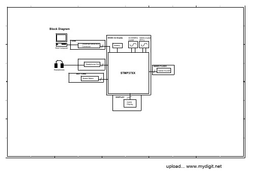
Sigmatel STMP3710方案MP3电路原理图
PREV
B
NEXT
VOL+
VOL-
LCD_CS LCD_RS LCD_RESET LCD_WR LCD_BUSY LCD_RD PWM0 PWM1 PWM2 PWM3 PWM4
28 41 42 43 27 44 91 87 83 84 82
LCD_CS LCD_RS LCD_RESET LCD_WR LCD_RD VDDIO_P
"Menu" & USB Recovery Mode
SW2 R3 1K PSWITCH SW PUSHBUTTON R4 100K 10%
VDDXTAL
GND 73 68 67 VDDXTAL REFP VAG
C
VDDXTAL
"Power/Play/ Pause Button"
C29 0.1uF
C30 0.1uF GND
Y2 32.768kHz 30ppm C36 XpF C37 XpF
RTC_XTALI RTC_XTALO
I2C_SDA I2C_SCL ROTARYB ROTARYA
80 81 25 24
R18 R19
0/NC 0/NC
I2C_SDA I2C_SCL
D18 LED
D17 LED
D10 LED
D12 LED
The 24 MHz crystal should be located close to the STMP37XX. Consult crystal manufacturer datasheet for recommended load capacitor values (typically 10-18pF). Cload = [ (C26*C27) / (C26+C27) ] + Cstray where Cstray = stray PCB capacitance, typically 4 - 6 pF Note: For Microsoft DRM applications use a 30 ppm crystal. NOTE: The crystal load capacitors C26 and C27, should be resized appropriately when STFM1000 is connected to the crystal circuit. Note that STFM1000 TB2 has 1-2 pF of internal capacitance.
MAX232中文资料
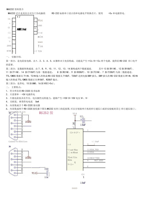
RS252 接C2+ 8 Cl* >n ci * Tl wit Tliw:上]m Rloat T2«it T2in R2inQV+ § v-1宁]OuF3 |11 EDA_TXD 12 EDA10 MCU^TXD 9 MC7_RXD £Cl I1DGKD• JCh1、* 2旦Cl 3 AMXlAd14C2+ 4C2-V- ''b20UIR?IN 8―-JVccGNDr i<-uiminWldUlTinT2NMAX232资料简介MAX232芯片是美信公司专门为电脑的RS-232标准串口设计的单电源电平转换芯片,使用 +5v 单电源供电。
一、 引脚介绍:第一部分:是电荷泵电路。
由1、2、3、4、5、6脚和4只电容构成。
功能是产生 +12v 和-12v 两个电源,提供给 RS-232 串口电平的需要。
第二部分:是数据转换通道。
由7、8、9、10、11、12、13、14脚构成两个数据通道。
其中13脚(R1IN)、12脚(R1OUT)、11 脚(T1IN)、14 脚(T1OUT)为第一数据通道。
8 脚(R2IN)、9 脚(R2OUT)、10 脚(T2IN)、7 脚(T2OUT)为第二数据通道。
TTL/CMOS 数据从T1IN 、T2IN 输入转换成 RS-232数据从T1OUT 、T2OUT 送到电脑 DB9插头;DB9插头的RS-232 数据从R1IN 、R2IN输入转换成 TTL/CMOS 数据后从 R1OUT 、R2OUT 输出。
第三部分:是供电。
15脚GND 、16脚VCC(+5v)。
二、 主要特点:1、 符合所有的RS-232C 技术标准2、 只需要单一 +5V 电源供电3、 片载电荷泵具有升压、电压极性反转能力,能够产生 +10V 和-10V 电压V+、V-4、 功耗低,典型供电电流 5mA5、 内部集成2个RS-232C 驱动器6、 内部集成两个 RS-232C 接收器下图为 MX232双串口的连接图,可以分别接单片机的串行通信口或者实验板的其它 串行通信接口 :Coimtcl To EDA CoreV5.0C13Connect To At 灿袅」三、max232应用电路,注意电容接法。
37103510系列37113511系列

光纤通讯传输系统用户手册Infinova目录注意事项 (1)产品描述 (2)订购信息 (3)安装 (3)电源 (4)发射机面板 (6)迷你发射机面板 (7)接收机面板 (8)典型系统连接图 (9)网管功能 (10)浪涌保护 (11)注意事项本产品应由专业的技术人员安装。
非专业人员请勿擅自安装操作。
如果在产品的安装过程中需要相关信息或服务,请和当地供应商联系,或者请拨打Infinova客户服务专线:1-732-355-9100,51 Stouts Lane, Monmouth Junction, NJ 08852 U.S.A。
注意:在返送任何产品进行维修前,请务必索取返修授权号码和填写货运通知单。
在该保证书中我们的责任只限于对我们的产品进行维修或替换,条件是产品在规定的额定值和应用范围内使用,及产品按照标准的工程准则使用,并且产品经过我们的检验证明是存在缺陷的。
由于意外,误用,滥用,疏忽,不合法的应用或安装,不合法的操作或维修,连接到不正确的电源电压或已改变的材料,或在非Infinova授权的维修中心进行维修的任何Infinova产品不在此保证书之列。
由美国Infinova公司提供的信息准确可靠。
但是,对于信息的使用,或对于由信息的使用可能导致的对第三方其它权利的任何侵害,Infinova一概不承担责任。
Infinova 公司的任何专利或专利权均不以暗示或其它方式颁发许可证。
警告:本产品应严加保护,防火,防震,谨防雨淋,谨防在潮湿环境中工作!通电状态下请勿向光学端口内观看,以免损伤眼睛!产品描述描述3710/3711和3510/3511系列光端机是在一根光纤上传输数字编码复合视频信号的高质量高可靠性光纤传输系统。
模块兼容PAL 、SECAM 和NTSC 视频信号。
即插即用的设计确保安装简便,无需电气或光学调节。
每台发射机或接收机都配置有状态指示灯,用于指示系统的运行状况。
该系列光端机提供独立式,插卡式和迷你型发射机三款供选择。
USB总线接口芯片CH371中文手册
USB总线接口芯片CH371中文手册(第二版)南京沁恒电子有限公司TEL: 025-*******FAX: 025-*******CH371是一个USB总线的通用接口芯片。
在本地端,CH371具有8位数据总线和读、写、片选控制线以及中断输出,可以方便地挂接到单片机、DSP、MCU等控制器的系统总线上;在计算机系统中,CH371的配套软件提供了简洁易用的操作接口,与本地端的单片机通讯就如同读写硬盘中的文件。
CH371屏蔽了USB通讯中的所有协议,在计算机应用层与本地端控制器之间提供端对端的连接。
基于CH371,不需要了解任何USB协议或者固件程序甚至驱动程序,就可以轻松地将并口、串口的产品升级到USB接口。
2、特点●屏蔽USB协议,在计算机应用层与本地端之间提供端对端的连接。
●两种通讯模式:单向数据流模式、请求加应答模式,支持伪中断。
●自动完成USB配置过程,完全不需要本地端控制器作任何处理。
●标准的USB V1.1接口,即插即用,D+引脚内置上拉电阻。
●内置4个端点,支持USB的控制传输、批量传输、中断传输。
●通用Windows驱动程序,提供设备级接口和应用层接口。
●通用的本地8位数据总线,4线控制:读选通、写选通、片选输入、中断输出。
●占用16个地址,可选直接地址方式或者复用地址方式。
●内置输入输出缓冲区,以中断方式通知本地端控制器传输数据。
●内置硬件实现的I2C主接口,应用层可以直接读写外挂的I2C从设备。
●在主控方式下可以提供16根输入信号线或者12根独立控制的输出信号线。
●内置上电复位,提供高电平有效复位输出和低电平有效复位输出。
●内置可选的看门狗电路Watch-Dog,为本地端控制器提供监控。
●可选多种封装:DIP28、SOP28、DIP24、CHIP。
●底层协议说明以及整体方案请索取相关资料(需签署技术保密协议)。
封装形式宽度引脚间距说明SOP28 7.62mm 300mil 1.27mm 50mil 标准的28脚贴片DIP28 15.24mm 600mil 2.54mm 100mil 标准的28脚双列直插DIP24S 7.62mm 300mil 2.54mm 100mil 标准的窄24脚双列直插4、引脚28脚封装的引脚号24脚封装的引脚号引脚名称类型引脚说明28 24 VCC 电源正电源12 9 GND 电源接地14 11 XI 输入晶体振荡的输入端,带偏置电阻13 10 XO 输出晶体振荡的反相输出端10 7 D+ 双向USB D+数据线,内置上拉电阻可控11 8 D- 双向USB D-数据线9 6 OFF 输入关闭D+上拉电阻,高有效,带下拉22~15 19~12 D7~D0 双向8位双向数据总线,带上拉,直接输入和独立控制输出4 4 RD# 输入读选通输入,低有效,带上拉,同时用于看门狗的清除输入3 3 WR# 输入写选通输入,低有效,带上拉27 23 CS# 输入片选输入,低有效,带下拉2 2 ALE 输入地址锁存使能,高有效,带上拉,下降沿锁存数据总线的复用地址1 1 INT# 输出中断输出,传输成功,低有效5~85部分支持A3~A0 双向4位地址线输入,带上拉,直接输入和独立控制输出24 21 SCL 输出I2C接口的时钟线23 20 SDA 双向I2C接口的数据线,开漏输出带上拉25 22 RST 输出上电复位和看门狗复位,高有效26 不支持RST# 输出上电复位和看门狗复位,低有效5.1. 一般说明本手册中的数据,以B结尾的为二进制数,以H结尾的为十六进制数,否则为十进制数,标注为x的位表示该位可以是任意值。
西门子产品型号详细说明

西门⼦产品型号详细说明详细说明S7-200系列定货号注释CPU6ES7 211-0AA23-0XB0 CPU221 DC/DC/DC,6输⼊/4输出6ES7 211-0BA23-0XB0 CPU221 继电器输出,6输⼊/4输出6ES7 212-1AB23-0XB8 CPU222 DC/DC/DC,8输⼊/6输出6ES7 212-1BB23-0XB8 CPU222 继电器输出,8输⼊/6输出6ES7 214-1AD23-0XB8 CPU224 DC/DC/DC,14输⼊/10输出6ES7 214-1BD23-0XB8 CPU224 继电器输出,14输⼊/10输出6ES7 214-2AD23-0XB8 CPU224XP DC/DC/DC,14DI/10DO,2AI/1AO6ES7 214-2BD23-0XB8 CPU224XP 继电器输出,14DI/10DO,2AI/1AO6ES7 216-2AD23-0XB8 CPU226 DC/DC/DC,24输⼊/16输出6ES7 216-2BD23-0XB8 CPU226 继电器输出,24输⼊/16输出扩展模块6ES7 221-1BH22-0XA8 EM221 16⼊ 24VDC,开关量6ES7 221-1BF22-0XA8 EM221 8⼊ 24VDC,开关量6ES7 221-1EF22-0XA0 EM221 8⼊ 120/230VAC,开关量6ES7 222-1BF22-0XA8 EM222 8出 24VDC,开关量6ES7 222-1EF22-0XA0 EM222 8出 120V/230VAC,0.5A 开关量6ES7 222-1HF22-0XA8 EM222 8出继电器6ES7 222-1BD22-0XA0 EM222 4出 24VDC 固态-MOSFET6ES7 222-1HD22-0XA0 EM222 4出继电器⼲触点6ES7 223-1BF22-0XA8 EM223 4⼊/4出 24VDC,开关量6ES7 223-1HF22-0XA8 EM223 4⼊ 24VDC/4出继电器6ES7 223-1BH22-0XA8 EM223 8⼊/8出 24VDC,开关量6ES7 223-1PH22-0XA8 EM223 8⼊ 24VDC/8出继电器6ES7 223-1BL22-0XA8 EM223 16⼊/16出 24VDC,开关量6ES7 223-1PL22-0XA8 EM223 16⼊ 24VDC/16出继电器6ES7 223-1BM22-0XA8 EM223 32⼊/32出 24VDC,开关量6ES7 223-1PM22-0XA8 EM223 32⼊ 24VDC/32出继电器6ES7 231-0HC22-0XA8 EM231 4⼊*12位精度,模拟量6ES7 231-7PB22-0XA8 EM231 2⼊*热电阻,模拟量6ES7 231-7PD22-0XA8 EM231 4⼊*热电偶,模拟量6ES7 232-0HB22-0XA8 EM232 2出*12位精度,模拟量6ES7 235-0KD22-0XA8 EM235 4⼊/1出*12位精度,模拟量6ES7 277-0AA22-0XA0 EM277 PROFIBUS-DP接⼝模块6GK7 243-2AX01-0XA0 CP243-2 AS-i接⼝模块6ES7 253-1AA22-0XA0 EM253 位控模块6ES7 241-1AA22-0XA0 EM241 调制解调器模块6GK7 243-1EX00-0XE0 CP243-1 ⼯业以太⽹模块6GK7 243-1GX00-0XE0 CP243-1IT ⼯业以太⽹模块附件6ES7 291-8GF23-0XA0 MC291,新CPU22x存储器盒,64K6ES7 297-1AA23-0XA0 CC292,CPU22x时钟/⽇期电池盒6ES7 291-8BA20-0XA0 BC293,CPU22x电池盒6ES7 290-6AA20-0XA0 扩展电缆,I/O扩展,0.8⽶,CPU22x/EM6ES7 901-3CB30-0XA0 编程/通讯电缆,PC/PPI,带光电隔离,5-开关,5m6ES7 901-3DB30-0XA0 编程/通讯电缆,PC/PPI,带光电隔离,USB接⼝,5-开关6ES7 292-1AD20-0AA0 CPU22x/EM端⼦连接器块,7个端⼦,可拆卸6ES7 292-1AE20-0AA0 CPU22x/EM端⼦连接器块,12个端⼦,可拆卸6ES7 292-1AG20-0AA0 CPU22x/EM连接器块,18个端⼦,可拆卸6AV6 640-0AA00-0AX0 TD400C⽂本显⽰器6EP1 332-1SH31 专为S7-200 设计电源,24V/3.5A 可并联5个S7-300系列定货号注释电源模板6ES7 307-1BA00-0AA0 电源模块(2A)6ES7 307-1EA00-0AA0 电源模块(5A)6ES7 307-1KA01-0AA0 电源模块(10A)CPU6ES7 312-1AE13-0AB0 CPU312,32K内存6ES7 312-5BE03-0AB0 CPU312C,32K内存 10DI/6DO6ES7 313-5BF03-0AB0 CPU313C,64K内存 24DI/16DO / 4AI/2AO6ES7 313-6BF03-0AB0 CPU313C-2PTP,64K内存 16DI/16DO6ES7 313-6CF03-0AB0 CPU313C-2DP,64K内存 16DI/16DO6ES7 314-1AG13-0AB0 CPU314,96K内存6ES7 314-6BG03-0AB0 CPU314C-2PTP 96K内存 24DI/16DO / 4AI/2AO6ES7 314-6CG03-0AB0 CPU314C-2DP 96K内存 24DI/16DO / 4AI/2AO6ES7 315-2AG10-0AB0 CPU315-2DP, 128K内存6ES7 315-2EH13-0AB0 CPU315-2 PN/DP, 256K内存6ES7 317-2AJ10-0AB0 CPU317-2DP,512K内存6ES7 317-2EK13-0AB0 CPU317-2 PN/DP,1MB内存6ES7 318-3EL00-0AB0 CPU319-3 PN/DP,1.4M内存内存卡6ES7 953-8LF20-0AA0 SIMATIC Micro内存卡 64kByte(MMC)6ES7 953-8LG11-0AA0 SIMATIC Micro内存卡128KByte(MMC)6ES7 953-8LJ20-0AA0 SIMATIC Micro内存卡512KByte(MMC)6ES7 953-8LL20-0AA0 SIMATIC Micro内存卡2MByte(MMC)6ES7 953-8LM20-0AA0 SIMATIC Micro内存卡4MByte(MMC)6ES7 953-8LP20-0AA0 SIMATIC Micro内存卡8MByte(MMC)开关量模板6ES7 321-1BH02-0AA0 开⼊模块(16点,24VDC)6ES7 321-1BH10-0AA0 开⼊模块(16点,24VDC)6ES7 321-1BH50-0AA0 开⼊模块(16点,24VDC,源输⼊)6ES7 321-1BL00-0AA0 开⼊模块(32点,24VDC)6ES7 321-7BH01-0AB0 开⼊模块(16点,24VDC,诊断能⼒)6ES7 321-1EL00-0AA0 开⼊模块(32点,120VAC)6ES7 321-1FF01-0AA0 开⼊模块(8点,120/230VAC)6ES7 321-1FF10-0AA0 开⼊模块(8点,120/230VAC)与公共电位单独连接6ES7 321-1FH00-0AA0 开⼊模块(16点,120/230VAC)6ES7 321-1CH00-0AA0 开⼊模块(16点,24/48VDC)6ES7 321-1CH20-0AA0 开⼊模块(16点,48/125VDC)6ES7 322-1BH01-0AA0 开出模块(16点,24VDC)6ES7 322-1BH10-0AA0 开出模块(16点,24VDC)⾼速6ES7 322-1CF00-0AA0 开出模块(8点,48-125VDC)6ES7 322-8BF00-0AB0 开出模块(8点,24VDC)诊断能⼒6ES7 322-5GH00-0AB0 开出模块(16点,24VDC,独⽴接点,故障保护)6ES7 322-1BL00-0AA0 开出模块(32点,24VDC)6ES7 322-1FL00-0AA0 开出模块(32点,120VAC/230VAC)6ES7 322-1BF01-0AA0 开出模块(8点,24VDC,2A)6ES7 322-1FF01-0AA0 开出模块(8点,120V/230VAC)6ES7 322-5FF00-0AB0 开出模块(8点,120V/230VAC,独⽴接点)6ES7 322-1HF01-0AA0 开出模块(8点,继电器,2A)6ES7 322-1HF10-0AA0 开出模块(8点,继电器,5A,独⽴接点)6ES7 322-1HH01-0AA0 开出模块(16点,继电器)6ES7 322-5HF00-0AB0 开出模块(8点,继电器,5A,故障保护)6ES7 322-1FH00-0AA0 开出模块(16点,120V/230VAC)6ES7 323-1BH01-0AA0 8点输⼊,24VDC;8点输出,24VDC模块6ES7 323-1BL00-0AA0 16点输⼊,24VDC;16点输出,24VDC模块模拟量模板6ES7 331-7KF02-0AB0 模拟量输⼊模块(8路,多种信号)6ES7 331-7KB02-0AB0 模拟量输⼊模块(2路,多种信号)6ES7 331-7NF00-0AB0 模拟量输⼊模块(8路,15位精度)6ES7 331-7NF10-0AB0 模拟量输⼊模块(8路,15位精度)4通道模式6ES7 331-7HF01-0AB0 模拟量输⼊模块(8路,14位精度,快速)6ES7 331-1KF01-0AB0 模拟量输⼊模块(8路, 13位精度)6ES7 331-7PF01-0AB0 8路模拟量输⼊,16位,热电阻6ES7 331-7PF11-0AB0 8路模拟量输⼊,16位,热电偶6ES7 332-5HD01-0AB0 模拟输出模块(4路)6ES7 332-5HB01-0AB0 模拟输出模块(2路)6ES7 332-5HF00-0AB0 模拟输出模块(8路)6ES7 332-7ND02-0AB0 模拟量输出模块(4路,15位精度)6ES7 334-0KE00-0AB0 模拟量输⼊(4路RTD)/模拟量输出(2路)6ES7 334-0CE01-0AA0 模拟量输⼊(4路)/模拟量输出(2路)附件6ES7 365-0BA01-0AA0 IM365接⼝模块6ES7 360-3AA01-0AA0 IM360接⼝模块6ES7 361-3CA01-0AA0 IM361接⼝模块6ES7 368-3BB01-0AA0 连接电缆 (1⽶)6ES7 368-3BC51-0AA0 连接电缆 (2.5⽶)6ES7 368-3BF01-0AA0 连接电缆 (5⽶)6ES7 368-3CB01-0AA0 连接电缆 (10⽶)6ES7 390-1AE80-0AA0 导轨(480mm)6ES7 390-1AF30-0AA0 导轨(530mm)6ES7 390-1AJ30-0AA0 导轨(830mm)6ES7 390-1BC00-0AA0 导轨(2000mm)6ES7 392-1AJ00-0AA0 20针前连接器6ES7 392-1AM00-0AA0 40针前连接器功能模板6ES7 350-1AH03-0AE0 FM350-1 计数器功能模块6ES7 350-2AH00-0AE0 FM350-2 计数器功能模块6ES7 351-1AH01-0AE0 FM351 定位功能模块6ES7 352-1AH02-0AE0 FM352 电⼦凸轮控制器+组态包光盘6ES7 355-0VH10-0AE0 FM355C 闭环控制模块6ES7 355-1VH10-0AE0 FM355S 闭环控制系统6ES7 355-2CH00-0AE0 FM355-2C 闭环控制模块6ES7 355-2SH00-0AE0 FM355-2S 闭环控制模块6ES7 338-4BC01-0AB0 SM338绝对位置输⼊模块6ES7 352-5AH00-0AE0 FM352-5⾼速布尔处理器6ES7 352-5AH00-7XG0 FM352-5功能软件包通讯模板6ES7 340-1AH02-0AE0 CP340 通讯处理器(RS232)6ES7 340-1BH02-0AE0 CP340 通讯处理器(20mA/TTY)6ES7 340-1CH02-0AE0 CP340 通讯处理器(RS485/RS422)6ES7 341-1AH01-0AE0 CP341 通讯处理器(RS232)6ES7 341-1BH01-0AE0 CP341 通讯处理器(20mA/TTY)6ES7 341-1CH01-0AE0 CP341 通讯处理器(RS485/RS422)6ES7 870-1AA01-0YA0 可装载驱动 MODBUS RTU 主站6ES7 870-1AB01-0YA0 可装载驱动 MODBUS RTU 从站6ES7 902-1AB00-0AA0 RS232电缆 5m6ES7 902-1AC00-0AA0 RS232电缆 10m6ES7 902-1AD00-0AA0 RS232电缆 15m6ES7 902-2AB00-0AA0 20mA/TTY电缆 5m6ES7 902-2AC00-0AA0 20mA/TTY电缆 10m6ES7 902-2AG00-0AA0 20mA/TTY电缆 50m6ES7 902-3AB00-0AA0 RS485/RS422电缆 5m6ES7 902-3AC00-0AA0 RS485/RS422电缆 10m6ES7 902-3AG00-0AA0 RS485/RS422电缆 50m6GK7 342-5DA02-0XE0 CP342-5通讯模块6GK7 342-5DF00-0XE0 CP342-5 光纤通讯模块6GK7 343-5FA01-0XE0 CP343-5通讯模块6GK7 343-1EX30-0XE0 CP343-1 以太⽹通讯模块6GK7 343-1EX21-0XE0 CP343-1 以太⽹通讯模块6GK7 343-1CX00-0XE0 CP343-1 以太⽹通讯模块6GK7 343-1CX10-0XE0 CP343-1 以太⽹通讯模块6GK7 343-1GX20-0XE0 CP343-1 IT 以太⽹通讯模块6GK7 343-1GX21-0XE0 CP343-1 IT 以太⽹通讯模块(⽀持PROFINET) 6GK7 343-1HX00-0XE0 CP343-1PN PROFINET以太⽹通讯模块6GK7 343-2AH00-0XA0 CP343-2 AS-Interface常⽤配件及附件对应型号:6XV1-830-0EH10 紫⾊电缆 2芯屏蔽(总线电缆或PROFIBUS电缆)。
- 1、下载文档前请自行甄别文档内容的完整性,平台不提供额外的编辑、内容补充、找答案等附加服务。
- 2、"仅部分预览"的文档,不可在线预览部分如存在完整性等问题,可反馈申请退款(可完整预览的文档不适用该条件!)。
- 3、如文档侵犯您的权益,请联系客服反馈,我们会尽快为您处理(人工客服工作时间:9:00-18:30)。
LM3710/LM3711Microprocessor Supervisory Circuits with Power Fail Input,Low Line Output,Manual Reset and Watchdog TimerGeneral DescriptionThe LM3710/LM3711series of microprocessor supervisory circuits provide the maximum flexibility for monitoring power supplies and battery controlled functions in systems without backup batteries.The LM3710/LM3711series are available in MSOP-10and 9-bump micro SMD packages.Built-in features include the following:Reset:Reset is asserted during power-up,power-down,and brownout conditions.RESET is guaranteed down to V CC of 1.0V.Manual Reset Input:An input that asserts reset when pulled low.Power-Fail Input:A 1.225V threshold detector for power fail warning,or to monitor a power supply other than V CC .Low Line Output:This early power failure warning indicator goes low when the supply voltage drops to a value which is 2%higher than the reset threshold voltage.Watchdog Timer:The WDI (Watchdog Input)monitors one of the µP’s output lines for activity.If no output transition occurs during the watchdog timeout period,reset is activated.Featuresn Standard Reset Threshold voltage:3.08Vn Custom Reset Threshold voltages:For other voltages between 2.2V and 5.0V in 10mV increments,contact National Semiconductor Corp.n No external components required n Manual-Reset inputn RESET (LM3710)or RESET (LM3711)outputs n Precision supply voltage monitorn Factory programmable Reset and Watchdog Timeout Delaysn Separate Power Fail comparatorn Available in micro SMD package for minimum footprint n ±0.5%Reset threshold accuracy at room temperature n ±2%Reset threshold accuracy over temperature extremesn Reset assertion down to 1V V CC (RESET option only)n 28µA V CC supply currentApplicationsn Embedded Controllers and Processors n Intelligent Instruments n Automotive SystemsnCritical µP Power MonitoringTypical Application20011803January 2005LM3710/LM3711Microprocessor Supervisory Circuits with Power Fail Input,Low Line Output,Manual Reset and Watchdog Timer©2005National Semiconductor Corporation Connection DiagramMSOP-10Top View(looking from the coating side)micro SMD 9Bump PackageBPA092001180220011801Pin DescriptionsPin Functionmicro SMD MSOP A12MR Manual-Reset input.When MR is less than V MRT (Manual Reset Threshold)RESET/RESET is engaged.B11V CC Power Supply input.C110RESETReset Logic Output.Pulses low for t RP (Reset Timeout Period)when triggered,and stays low whenever V CC is below the reset threshold or when MR is below V MRT .It remains low for t RP after either V CC rises above the reset threshold,or after MR input rises above V MRT (LM3710only).RESETReset Logic Output.RESET is the inverse of RESET (LM3711only).C28PFO Power-Fail Logic Output.When PFI is below V PFT ,PFO goes low;otherwise,PFO remains high.C37LLOLow-Line Logic Output.Early Power-Fail warning output.Low when V CC falls below V LLOT (Low-Line Output Threshold).This output can be used to generate an NMI (Non-Maskable Interrupt)to provide an early warning of imminent power-failure.B35GND Ground reference for all signals.A34WDI Watchdog Input Transition Monitor:If no transition activity occurs for a period exceeding t WD (Watchdog Timeout Period),reset is engaged.A23PFI Power-Fail Comparator Input.When PFI is less than V PFT (Power-Fail Reset Threshold),the PFO goes low;otherwise,PFO remains high.B26,9NCNo Connect.Test input used at factory only.Leave floating.L M 3710/L M 3711 2LM3710/LM3711 Block Diagram3Ordering Information20011804*For other voltages between 2.2V and 5.0V,please contact National Semiconductor sales office.LM3710/LM3711Part Number Output Reset Timeout Period Watchdog Timeout Period Package Package Marking MSOPmicro SMD LM3710XKBP-232totem-pole 28ms 102ms x %%I19LM3710XKBPX-232totem-pole 28ms 102ms x %%I19LM3710XKBP-463totem-pole 28ms 102ms x %%I21LM3710XKBPX-463totem-pole 28ms 102ms x%%I21LM3710XKMM-232totem-pole 28ms 102ms x R72B LM3710XKMMX-232totem-pole 28ms 102ms x R72B LM3710XKMM-463totem-pole 28ms 102ms x R74B LM3710XKMMX-463totem-pole 28ms 102ms x R74B LM3710XNMM-450totem-pole 1.4ms 1600ms x R84B LM3710XNMMX-450totem-pole 1.4ms 1600ms x R84B LM3710XNMM-470totem-pole 1.4ms 1600ms x R83B LM3710XNMMX-470totem-pole 1.4ms 1600ms xR83B LM3710XQBP-308totem-pole 200ms 1600ms x %%IA LM3710XQBPX-308totem-pole 200ms 1600ms x%%IA LM3710YQMM-232open-drain 200ms 1600ms x R77B LM3710YQMMX-232open-drain 200ms 1600ms xR77B LM3711XKBP-232totem-pole 28ms 102ms x %%I20LM3711XKBPX-232totem-pole 28ms 102ms x %%I20LM3711XKBP-463totem-pole 28ms 102ms x %%I22LM3711XKBPX-463totem-pole 28ms 102ms x%%I22LM3711XKMM-232totem-pole 28ms 102ms x R73B LM3711XKMMX-232totem-pole 28ms 102ms x R73B LM3711XKMM-463totem-pole 28ms 102ms x R75B LM3711XKMMX-463totem-pole 28ms 102ms x R75B LM3710XQMM-308totem-pole200ms1600msxR37BL M 3710/L M 37114Ordering Information(Continued)LM3710/LM3711(Continued)Part Number OutputResetTimeoutPeriodWatchdogTimeoutPeriodPackagePackageMarkingMSOPmicroSMDLM3710XQMMX-308totem-pole200ms1600ms x R37B LM3711XQBP-308totem-pole200ms1600ms x%%IB LM3711XQBPX-308totem-pole200ms1600ms x%%IB LM3711XQMM-308totem-pole200ms1600ms x R38B LM3711XQMMX-308totem-pole200ms1600ms x R38B %%is the datecode and will vary with time.Table Of FunctionsPart Number ActiveLowResetActiveHighResetOutput(X=totem-pole)(Y=open-drain)ResetTimeoutPeriodWatchdogTimeoutPeriodManualResetPower FailComparatorLowLineOutputLM3710x X,Y*Customized Customized x x xLM3711x X Customized Customized x x x*=available upon request.Contact NationalLM3710/LM37115Absolute Maximum Ratings (Note 1)If Military/Aerospace specified devices are required,please contact the National Semiconductor Sales Office/Distributors for availability and specifications.Supply Voltage (V CC )−0.3V to 6.0VAll Other Inputs −0.3V to V CC +0.3VESD Ratings (Note 2)Human Body Model Machine Model1.5kV 150VPower Dissipation (Note 3)Operating Ratings (Note 1)Temperature Range−40˚C ≤T J ≤85˚CLM3710/LM3711Series Electrical CharacteristicsLimits in the standard typeface are for T J =25˚C and limits in boldface type apply over full operating range.Unless otherwise specified:V CC =+2.2V to 5.5V.Symbol Parameter ConditionsMin TypMax UnitsPOWER SUPPLYV CC Operating Voltage Range:V CC LM3710 1.0 5.5V LM37111.25.5I CCV CC Supply CurrentAll inputs =V CC ;all outputs floating2850µARESET THRESHOLD V RSTReset ThresholdV CC falling−0.5−2V RST+0.5+2%V CC falling:T A =0˚C to 70˚C−1.5+1.5V RSTH Reset Threshold Hysteresis 0.0032•V RSTmV t RPReset Timeout PeriodReset Timeout Period =E,J,N,S Reset Timeout Period =F,K,P,T Reset Timeout Period =G,L,Q,U ResetTimeoutPeriod=H,M,R,V1201401120 1.42820016002402802240mst RDV CC to Reset Delay V CC falling at 1mV/µs20µsRESET (LM3711)V OLRESETV CC >2.25V,I SINK =900µA 0.3VV CC >2.7V,I SINK =1.2mA 0.3V CC >4.5V,I SINK =3.2mA0.4V OHRESETV CC >1.2V,I SOURCE =50µA 0.8V CC VV CC >1.8V,I SOURCE =150µA 0.8V CC V CC >2.25V,I SOURCE =300µA 0.8V CC V CC >2.7V,I SOURCE =500µA 0.8V CC V CC >4.5V,I SOURCE =800µAV CC −1.5VI LKGOutput Leakage Current V RESET =5.5V1.0µA RESET (LM3710)V OLRESETV CC >1.0V,I SINK =50µA 0.3VV CC >1.2V,I SINK =100µA 0.3V CC >2.25V,I SINK =900µA 0.3V CC >2.7V,I SINK =1.2mA 0.3V CC >4.5V,I SINK =3.2mA0.4V OHRESETV CC >2.25V,I SOURCE =300µA 0.8V CC V CC >2.7V,I SOURCE =500µA 0.8V CC V CC >4.5V,I SOURCE =800µAV CC −1.5VL M 3710/L M 3711 6LM3710/LM3711Series Electrical Characteristics(Continued)Limits in the standard typeface are for T J =25˚C and limits in boldface type apply over full operating range.Unless otherwise specified:V CC =+2.2V to 5.5V.Symbol ParameterConditionsMin TypMax Units WDI WDI Watchdog Input Current −1+1µAWDI T Watchdog Input Threshold 0.2•V CC 1.2250.8•V CC Vt WDWatchdogTimeout PeriodWatchdog Timeout Period =E,F,G,H Watchdog Timeout Period =J,K,L,M Watchdog Timeout Period =N,P,Q,R WatchdogTimeoutPeriod=S,T,U,V4.371112017900 6.21021600256009.3153240038400msPFI/MR V PFT PFI Input Threshold 1.2001.2251.250VV MRT MR Input Threshold MR,Low 0.8V MR,High2.0V PFTH /V MRTH PFI/MR Threshold Hysteresis PFI/MR falling:V CC =V RSTMAXto 5.5V0.0032•V RSTmV I PFI Input Current (PFI only)−7575nA R MR MR Pull-up Resistance 355675k Ωt MD MR to Reset Delay12µS t MR MR Pulse Width25µSPFO,LLO V OLPFO,LLO Output VoltageV CC >2.25V,I SINK =900µA 0.3VV CC >2.7V,I SINK =1.2mA 0.3V CC >4.5V,I SINK =3.2mA0.4V OHV CC >2.25V,I SOURCE =300µA 0.8V CC V CC >2.7V,I SOURCE =500µA 0.8V CC V CC >4.5V,I SOURCE =800µAV CC −1.5VLLO OUTPUT V LLOTLLO Output Threshold(V LLO −V RST ,V CC falling) 1.01•V RST1.02•V RST1.03•V RSTVV LLOTH Low-Line Comparator Hysteresis 0.0032•V RSTmVt CDLow-LineComparator DelayV CC falling at 1mV/µs20µsLM3710/LM37117LM3710/LM3711Series Electrical Characteristics(Continued)Note 1:Absolute Maximum Ratings indicate limits beyond which damage to the device may occur.Operating Ratings indicate conditions for which the device is intended to be functional,but do not guarantee specific performance limits.For guaranteed specifications and test conditions,see the Electrical Characteristics.The guaranteed specifications apply only for the test conditions listed.Some performance characteristics may degrade when the device is not operated under the listed conditions.Note 2:The Human Body model is a 100pF capacitor discharged through a 1.5k Ωresistor into each pin.The machine model is a 200pF capacitor discharged directly into each pin.Note 3:The maximum allowable power dissipation is a function of the maximum junction temperature,T J (MAX),the junction-to-ambient thermal resistance,θJ-A ,and the ambient temperature,T A .The maximum allowable power dissipation at any ambient temperture is calculated using:Where the value of θJ-A for the MSOP-10package is 195˚C/W in a typical PC board mounting and the micro SMD package is 220˚C/W.L M 3710/L M 3711 8Typical Performance CharacteristicsSupply Current vs Supply Voltage3.3V Supply Current vs Temperature2001181520011811Normalized Reset Threshold Voltage vs TemperatureReset Timeout Period vs V CC2001181220011832Reset Timeout Period vs TemperatureMax.Transient Duration vs Reset Comparator Overdrive(V CC =3.3V)2001181020011816LM3710/LM37119Typical Performance Characteristics(Continued)Watchdog Timeout Period vs Temperature(t WD programmed as 6.2ms)Low-Line Comparator Propagation Delay vs Temperature2001181320011814L M 3710/L M 3711 10Circuit InformationRESET OUTPUTThe Reset input of a µP initializes the device into a known state.The LM3710/LM3711microprocessor supervisory cir-cuits assert a forced reset output to prevent code execution errors during power-up,power-down,and brownout condi-tions.RESET is guaranteed valid for V CC >1V.Once V CC ex-ceeds the reset threshold,an internal timer maintains the output for the reset timeout period.After this interval,reset goes high.The LM3710offers an active-low RESET;The LM3711offers an active-high RESET.Any time V CC drops below the reset threshold (such as during a brownout),the reset activates.When V CC again rises above the reset threshold,the internal timer starts.Reset holds until V CC exceeds the reset threshold for longer than the reset timeout period.After this time,reset releases.The Manual Reset input (MR)will initiate a forced reset also.See the Manual Reset Input section.RESET THRESHOLDThe LM3710/LM3711family is available with a reset voltage of 3.08V.Other reset thresholds in the 2.20V to 5.0V range,in steps of 10mV,are available;contact National Semicon-ductor for details.MANUAL RESET INPUT (MR)Many µP-based products require a manual reset capability,allowing the operator to initiate a reset.The MR input is fully debounced and provides an internal 56k Ωpull-up.When the MR input is pulled below V MRT (1.225V)for more than 25µs,reset is asserted after a typical delay of 12µs.Reset remains active as long as MR is held low,and releases after the reset timeout period expires after MR rises above V MRT .Use MR with digital logic to assert or to daisy chain supervisory circuits.It may be used as another low-line comparator by adding a buffer.POWER-FAIL COMPARATOR (PFI/PFO)The PFI is compared to a 1.225V internal reference,V PFT .If PFI is less than V PFT ,the Power Fail Output PFO drops low.The power-fail comparator signals a falling power supply,and is driven typically by an external voltage divider that senses either the unregulated supply or another system supply voltage.The voltage divider generally is chosen so the voltage at PFI drops below V PFT several milliseconds before the main supply voltage drops below the reset thresh-old,providing advanced warning of a brownout.The voltage threshold is set by R 1and R 2and is calculated as follows:Note this comparator is completely separate from the rest of the circuitry,and may be employed for other functions as needed.LOW-LINE OUTPUT (LLO)The low-line output comparator is typically used to provide a non-maskable interrupt to a µP when V CC begins falling.LLO monitors V CC and goes low when V CC falls below V LLOT (typically 1.02•V RST )with hysteresis of 0.0032•V RST .WATCHDOG TIMER INPUT (WDI)The watchdog timer input monitors one of the microproces-sor’s output lines for activity.Each time a transition occurs on this monitored line,the watchdog counter is reset.However,if no transition occurs and the timeout period is reached,the LM3710/LM3711assumes that the microprocessor has locked up and the reset output is activated.WDI is a high impedance input.SPECIAL PRECAUTIONS FOR THE MICRO SMD PACKAGEAs with most integrated circuits,the LM3710and LM3711are sensitive to exposure from visible and infrared (IR)light radiation.Unlike a plastic encapsulated IC,the micro SMD package has very limited shielding from light,and some sensitivity to light reflected from the surface of the PC board or long wavelength IR entering the die from the side may be experienced.This light could have an unpredictable affect on the electrical performance of the IC.Care should be taken to shield the device from direct exposure to bright visible or IR light during operation.MICRO SMD MOUNTINGThe micro SMD package requires specific mounting tech-niques which are detailed in National Semiconductor Appli-cation Note AN-1112.Referring to the section Surface Mount Technology (SMT)Assembly Considerations ,it should be noted that the pad style which must be used with the 9-pin package is the NSMD (non-solder mask defined)type.For best results during assembly,alignment ordinals on the PC board may be used to facilitate placement of the micro SMD device.LM3710/LM371111Timing Diagrams20011828FIGURE 1.LM3710/LM3711Reset Time with MR and WDI20011829FIGURE 2.LLO Output20011830FIGURE 3.PFI Comparator Timing DiagramL M 3710/L M 3711 12Typical Application Circuits20011818FIGURE 4.Monitoring Two Critical Supplies And Dataline20011819FIGURE 5.Monitoring Two Supplies plus Manual Reset And DatalineLM3710/LM371113Typical Application Circuits(Continued)20011820FIGURE 6.Monitoring Dual Supplies plus External Fault Input And Dataline20011821Note:MR input with its 1.225V nominal threshold,may monitor an additional supply voltage.An internal 56k Ωpull-up resistor is included on this input.FIGURE 7.Microprocessor Supervisor with Early Warning DetectorL M 3710/L M 3711 14LM3710/LM3711 Typical Application Circuits(Continued)20011840FIGURE8.LM3710Long Period oscillator15Physical Dimensionsinches (millimeters)unless otherwise noted10Lead MSOP Package NS Package Number MUB10AL M 3710/L M 3711 16LM3710/LM3711 Physical Dimensions inches(millimeters)unless otherwise noted(Continued)NOTES:UNLESS OTHERWISE SPECIFIED1.EPOXY COATING2.63Sn/37Pb EUTECTIC BUMP3.RECOMMEND NON-SOLDER MASK DEFINED LANDING PAD.4.PIN1IS ESTABLISHED BY LOWER LEFT CORNER WITH RESPECT TO TEXT ORIENTATION.REMAINING PINS ARE NUMBERED COUNTERCLOCKWISE.5.XXX IN DRAWING NUMBER REPRESENTS PACKAGE SIZE VARIATION WHERE X1IS PACKAGE WIDTH,X2IS PACKAGE LENGTH AND X3ISPACKAGE HEIGHT.6.NO JEDEC REGISTRATION AS OF AUG.1999.9bump micro SMD PackageNS Package Number BPA09FFBThe dimensions of X1,X2and X3are given belowX1=1.412mmX2=1.412mmX3=0.850mm17NotesNational does not assume any responsibility for use of any circuitry described,no circuit patent licenses are implied and National reserves the right at any time without notice to change said circuitry and specifications.For the most current product information visit us at .LIFE SUPPORT POLICYNATIONAL’S PRODUCTS ARE NOT AUTHORIZED FOR USE AS CRITICAL COMPONENTS IN LIFE SUPPORT DEVICES OR SYSTEMS WITHOUT THE EXPRESS WRITTEN APPROVAL OF THE PRESIDENT AND GENERAL COUNSEL OF NATIONAL SEMICONDUCTOR CORPORATION.As used herein:1.Life support devices or systems are devices or systems which,(a)are intended for surgical implant into the body,or (b)support or sustain life,and whose failure to perform when properly used in accordance with instructions for use provided in the labeling,can be reasonably expected to result in a significant injury to the user.2.A critical component is any component of a life support device or system whose failure to perform can be reasonably expected to cause the failure of the life support device or system,or to affect its safety or effectiveness.BANNED SUBSTANCE COMPLIANCENational Semiconductor certifies that the products and packing materials meet the provisions of the Customer Products Stewardship Specification (CSP-9-111C2)and the Banned Substances and Materials of Interest Specification (CSP-9-111S2)and contain no ‘‘Banned Substances’’as defined in CSP-9-111S2.National Semiconductor Americas Customer Support CenterEmail:new.feedback@ Tel:1-800-272-9959National SemiconductorEurope Customer Support CenterFax:+49(0)180-5308586Email:europe.support@Deutsch Tel:+49(0)6995086208English Tel:+44(0)8702402171Français Tel:+33(0)141918790National Semiconductor Asia Pacific Customer Support CenterEmail:ap.support@National SemiconductorJapan Customer Support Center Fax:81-3-5639-7507Email:jpn.feedback@ Tel:81-3-5639-7560L M 3710/L M 3711M i c r o p r o c e s s o r S u p e r v i s o r y C i r c u i t s w i t h P o w e r F a i l I n p u t ,L o w L i n e O u t p u t ,M a n u a l R e s e t a n d W a t c h d o g T i m e r。