UTC3414
UTC ASQR-01

11/21/03Page 1 of 12WARNINGThis document is the property of United T echnologies Corporation (UTC). You may not possess, use, copy or disclose this document or any information in it, for any purpose, including without limitation to design, manufacture, or repair parts, or obtain FAA or other government approval to do so, without UTC’s express written permission. Neither receipt nor possession of this document alone, from any source, constitutes such permission. Possession, use, copying or disclosure by anyone without UTC’s express written permission is not authorized and may result in criminal and/or civil liability.PURPOSE & SCOPE1.This specification defines supplier quality requirements as agreed upon by the following businessentities as members of the ASQR Common Specification Team herein referred to as “member”:Aftermarket Operations AOHamilton Sundstrand HSPratt & Whitney PWPratt & Whitney Canada PWCSikorsky Aircraft SACUTC Fuel Cells UTCFC2.This document applies to suppliers and all members of their supply chain who furnish product,material or services to any of the above members.3.Each member or their representatives and their customers including Government/regulatoryagencies, shall have the right of entry into a supplier’s facility or that of their subcontractors, access to quality records, quality system documentation, and the right to verify product and conduct audits.4.Changes to any paragraph in this document will be annotated by an asterisk (*) to the left of theaffected paragraph.5.References5.1ANSI/NCSL Z540–1Calibration Laboratories and Measuring & Test Equipment –General Requirements5.2ANSI/NCSL Z540–2U.S. Guide to the Expression of Uncertainty in Measurement 5.3ASQR–01 Form 3,Supplier Request for Information5.4ASQR–01 Form 4Quality Verification Checklist5.5ASQR – 09.1Flight Safety Parts Program5.6ASQR – 15.1Handling, Storage, Packaging, Preservation and Delivery5.7ASQR – 20.1Supplier Sampling Requirement5.8ISO 10012Quality Assurance Requirements for Measuring Equipment 5.9ISO 17025General Requirements for the Competence of Testing andCalibration Laboratories11/21/03Page 2 of 125.10RTCA/DO–178Software Considerations in Airborne Systems & EquipmentCertification5.11SAE AIR 5359Requirements for Registration of Quality Systems to AS9000or AS91005.12SAE AS 9100Quality Systems – Aerospace – Model for Quality Assurance inDesign, Development, Production, Installation and Servicing5.13SAE AS 9102Aerospace First Article Inspection Requirement5.14UTCQR – 09.1Process Certification Requirements6.Forms6.1ASQR–01 Form 3Supplier Request for Information (SRI)6.2ASQR–01 Form 4Quality Verification Checklist6.3AS 9102 Form 1First Article Inspection – Part Number Accountability6.4AS 9102 Form 2First Article Inspection – Product Accountability6.5AS 9102 Form 3First Article Inspection – Characteristic Accountability7.Nature of ChangesDocument was completely reformatted including appendices to incorporate the eight element structure defined in AS9100:2000. All requirements that are now covered in AS9100 were removed. Significant changes to the document include:F Cancellation of Appendices 1 through 3F Additional audit inspection requirementsF Eye exam requirements defined for two inspection criteriaF Registration to AS/EN/JIS Q 9100:2000 required by June 200411/21/03Page 3 of 12SECTION 11.Application1.1This document employs, as a foundation, SAE Aerospace Standard (AS)9100 Revision A whichincorporates International Standards Organization (ISO) 9001:2000 requirements and is supplemented by both common and unique business member requirements as defined herein.Suppliers and all members of their supply chain, must be compliant to AS9100 and all applicable common and unique requirements.1.2Suppliers who receive a Purchase Order from a UTC member company must be registered toAS/EN/JIS Q 9100 by June 30, 2004. In order to be compliant to this requirement, the Registration Accreditation Board (RAB) or an international equivalent must accredit the other party performing the registration. Additionally, the certificate of registration must specify that the registration activity was based on the requirements contained in the Aerospace Information Report – SAE AIR 5359. The supplier is responsible to provide the AS9100 Certificate of Registration to each UTC Member that issued a Purchase Order. The supplier is also responsible to provide each member with notification of any changes in the registration within 24 hours of receiving notification of the change.1.3Section II identifies common requirements in addition to the AS9100 standard. Deviations fromSection II requirements apply only to the member granting exception.1.4Section III identifies unique member requirements in addition to AS9100 and common requirements.Certain unique requirements may direct suppliers to use a specific UTC member document in place of an ASQR common document.1.5Supplier shall refer to the Specification Revision List date or the specification revisions identified onthe Purchase Order to determine the revision of the specification that applies. Requests for member–specific specifications that are needed shall be requested from the applicable member’s Procurement department.1.6It is the responsibility of the supplier to ensure that they are working to the latest version ofspecifications referenced within this document as well as Purchase Order requirements.Page 4 of 1211/21/031.7It is the responsibility of the supplier to obtain copies of non–UTC documents specified by this ASQR.These documents include, but may not be limited to, the following:DOCUMENT AVAILABLE FROMISO STANDARDS 1. Canadian SourceStandards Council of Canada350 Sparks StreetOttawa, OntarioK1R 7S8, Canada2. American SourceAmerican National Standards Institute11 West 42nd StreetNew York, New York 10036 U.S.A.3. European SourceInternational Organization for StandardizationCase Oistake 56CH–1211 Geneve 20SwitzerlandSAE SPECIFICATIONS Society of Automotive Engineers400 Commonwealth DriveWarrendale, PA 15096–0001, U.S.A.ANSI SPECIFICATIONS American Society for Quality611 East Wisconsin AvenueMilwaukee, WI 53201–3005, USARTCA/DO–178Radio Technical Commission for Aeronautics PublicationsRTCA SecretariatSuite 500, 1425 K Street N.W.Washington, D.C., 20005, USARegistration Accreditation Board(RAB)Registrar Accreditation Board 600 N. Plankinton Ave. Milwaukee, WI 5320311/21/03Page 5 of 12SECTION II – Additional Common Requirements1.ScopeNo additional requirements2.Normative ReferenceNo additional requirements3.Terms and DefinitionsNo additional requirements4.Quality Management System4.1Changes that may affect quality must be documented and communicated to the applicablemember(s) Quality Assurance Representative prior to effectivity of the change.EXAMPLE OF CHANGESOwnershipManufacturing locationProcess or inspection techniques4.2Each member has the individual right to disapprove a supplier’s Quality System as well as the QualitySystem of their subcontractors.4.3All communications between the supplier and the UTC member, Quality Systems Manual andProcedures as well as any process documentation which requires approval or source qualification by the UTC member must be written in the English language. In cases where the supplier maintains copies in their native language as well as in English and there is a conflict, the English language document shall take precedence.4.4Control of Quality Records4.4.1Retain quality records and make them available for the applicable retention period specifiedbelow. Electronic imaging/microfilming of records in lieu of storing actual inspection records ispermissible.F40 years from time of manufacture for flight safety, Space Shuttle fuel cells/main engine components, critical/major rotor parts (turbine and compressor disks, hubs, shafts, freeturbine couplings and turbine disk side plates) and any other articles which also require heatcode and suffix number identification; serialized major engine (cast/fabricated) cases (inlet,fan, compressor, intermediate, diffuser, combustion, turbine and exhaust cases) and mainshaft bearing supports, which are not integral to a major caseF10 years for all other parts except aftermarket and off–the–shelf/industry partsF8 years for aftermarket partsF 4 years for off–the–shelf/industry standard parts (i.e. AN, AS, MS, JAN, etc.)11/21/03Page 6 of 124.4.2Examples of records to be retained are, but not limited to:F Procurement documents (supplier placed orders)F Receiving inspection Records (e.g., test reports and material certifications)F Manufacturing/fabrication records (e.g. planning sheets, routers, etc.)F Process control records (used as acceptance criteria)F First article inspection reportsF In process/final inspection & test recordsF Radiographs, technique sheets and related acceptance reportsF Records of nonconforming material dispositionF Records of deliverable and nondeliverable software4.4.3Supplier shall retain radiographs for flight safety, critical/major rotor parts (turbine andcompressor disks, hubs, shafts, free turbine couplings and turbine disk side plates), SpaceShuttle fuel cells/main engine components and other articles which also require heat code andsuffix number identification as well as serialized major engine (cast/fabricated) cases, (i.e., inletfan, compressor, intermediate, diffuser, combustion, turbine and exhaust cases), and main shaftbearing supports which are not integral to a major case and engine components traceable byEngineering Drawing/Quality Assurance Data required serial numbers for 40 years.4.4.4Radiographs for parts where serial number traceability to the radiographs is maintained shall beretained for 10 years. Radiographs for those parts where serial number traceability to theradiographs is not maintained shall be retained for 10 years only if no other inspection record isretained that documents completion and final acceptance of radiographic inspection.4.4.5All quality records (non–electronic) shall be documented in ink or other permanent marking.Corrections to work instructions or documents must be recorded, dated and signed in ink or otherpermanent marking method with the original data being legible and retrievable after the change.4.4.6All electronic records must be controlled, retained, and retrievable per the same requirementsidentified for hard copy records. For electronic records that are transferred from computer files,the storage media must be capable of maintaining the data integrity for the full retention period.5.Management ResponsibilityNo additional requirements11/21/03Page 7 of 126.Resource Management6.1Unless otherwise specified, procedures shall be implemented to ensure that eye examinations,including visual acuity and color vision, as applicable, are administered to all individuals performing visual inspection by a medically qualified/trained person.6.1.1Individuals performing visual inspections on welds or nondestructive test (NDT) inspection shallhave the following vision in at least one eye, either corrected or uncorrected:Near Vision:Jaegar Type 1 or equivalentColor Vision:Must be able to distinguish and differentiate be-tween the colors used in the inspection, processactivity or NDT method performed. Testing forcolor vision is required one time only.6.1.2Individuals performing normal visual inspection (i.e. calibration, non–weld, inprocess, layout,dimensional) shall have the following vision in at least one eye, either corrected or uncorrected:Near Vision:Stellen14/18 or better (20/25 or better), JaegarType 2 at 14 inches or greater, Ortho–Rater 8 orequivalentColor Vision:Must be able to distinguish and differentiate be-tween the colors used in the method for whichcertification is required, process being performedor inspection activity. T esting for color vision isrequired one time only.6.1.3For individuals who do not meet the vision requirements in paragraph 6.1.2, supplier supervisionshall review each individual’s job assignment to determine if this assignment can be effectivelyperformed and to ensure these individuals do not perform inspection tasks where these visionrequirements are necessary in determining product conformance. The review by supervisionshall be documented and available for review upon request by a UTC member.6.1.4Eye exam intervals shall not exceed one year, and records shall be retained for each individual.7.Product Realization7.1Contract Review7.1.1Upon receipt of a UTC Member Purchase Order requiring Government Contract QualityAssurance (GCQA), promptly notify the Government Representative who services your facility,or, if there is none, the Government Inspection office nearest to your facility.7.1.2Verbal agreements or instructions are not allowed.11/21/03Page 8 of 127.2The use of directed sources does not relieve the responsibility for subcontractor control (i.e., anapproved source for Non–Destructive T esting, Plating, Coating, etc.).7.3Provide UTC members Supplier Quality Assurance with a World Wide Web internet e–mail addressbelonging to the supplier (not a private e–mail account) to permit communications with the suppliers quality department. The e–mail address and any changes shall be sent to the applicable UTC Member Supplier Quality Assurance (SQA) organization.7.4Where a member owns the design of an article purchased from a supplier (first–tier) who furthersubcontracts all or portions of that work to other subcontractors (second–tier), the first–tier supplier’s Purchase Order must state that the articles are for applicable member’s “end use” and must be controlled per applicable Purchase Order requirements.7.5Product identified with member acceptance symbols can only be shipped to the member or amember–approved destination.7.6Supplier Request for Information (SRI), ASQR–01 Form 3, shall be submitted to applicableProcurement personnel and may be used for items such as:F An anomaly noted in a drawing or specification that could result in a nonconformanceF Lack of clarity or definition in a drawing or specificationF A request for an alternate method to a quality system requirement. Any alternate methodsto a quality system requirement must receive approval from the applicable UTC Memberprior to incorporation.Note:SRIs are not used for processing product nonconformances.7.7Return all documents, records, gaging, stamps, or other customer supplied product upon writtennotification from UTC member or when business with the UTC member has ceased.7.8The use of an operator certification program or other special manufacturing methodologies (e.g.manufacturing controlling features, die/mold control, method of manufacturing, etc.) must be approved by the appropriate member via ASQR–01 SRI process.7.9Non–Deliverable Software:For software used in the manufacturing and inspection & testing of deliverable hardware or in the qualification or acceptance of deliverable software or hardware, procedures are required for implementation of the following:(a)Define the purpose or function of the software and how software requirements areinitiated, documented and approved.(b)Identify coding guidelines (i.e.: naming conventions, comments etc.) documentationand approval required for release test.(c)Define the process, documentation and approvals used to ensure requirements aremet. Ensure software cannot be modified without authorization.11/21/03Page 9 of 12(d)Define the process documentation and approvals required for release to use.Provide objective evidence that the software performs its required function prior touse. (Objective evidence requires recording and retaining variable data.)Inspection, review and approval of software responsible for finished part featuresmust be performed by someone acting in an acknowledged product integrity role.Part specific software used to verify quantitative values requires an independentmethod of validation, and correlation of the two sets of results. (Acceptablecorrelation requires the difference to be within 10% of the tolerance for eachcharacteristic. Differences greater than 10% but not exceeding 25% can beacceptable with documented justification. Differences greater than 25% are notacceptable).(e)Define the process and approvals required to control software and relateddocumentation, including revisions and identification for traceability purposes.(f)Define the process used to approve/accept software into various libraries, controlaccess and provide for backup and recovery. Master versions must be located ina secure location.(g)Identify the method for storage, handling and release of software to the user.(h)Define the process for identifying problems, analysis for problem cause,implementation and verification of corrective action.7.10Deliverable Software:7.10.1For software embedded in commercial deliverable hardware, maintain a quality system thatmeets the requirements of RTCA/DO–178.7.10.2Create a Software Quality Assurance Plan (SQAP) that will be reviewed and approved as definedby the Purchase Order.7.10.3Submit a Software Quality Assurance (SQA) Plan for review and approval by the applicablemember. All revisions must be submitted for review and approval.7.10.4The plan shall provide:(a) A description of the SQA environment, including scope, organizational responsibilitiesand interfaces, standards, procedures, tools and methods.(b) A statement of the SQA authority, responsibility and independence, including theapproval authority for software products.11/21/03Page 10 of 12(c)The SQA activities that are to be performed for each software life cycle process andthroughout the product development including,(1)SQA methods, for example, reviews, audits, reporting, inspections andmonitoring of the software life cycle processes.(2)Activities related to the problem reporting, tracking and corrective actionsystem.(3) A description of the method used to ensure disposition and retention of anyremaining SQA open action items and change requests, and completion of allsoftware development tasks at the conclusion of the program.(d)Identification of the plans used to establish the software development process, thesoftware verification process and the software configuration management process.(e) A definition of the records to be produced by the SQA process.(f) A method to ensure that master versions of such software are maintained in asecure location to prevent unauthorized modifications.7.11Certain processes that may affect the structural or functional integrity of parts or assemblies andwhere the results of these processes may not be fully verified by subsequent inspection are designated as special processes. When specified on the drawing or Purchase Order, suppliers must use only sources approved by the specific member company to perform these special processes (each special process supplier must obtain initial approval from each specific member company).7.12Suppliers must provide raw materials test reports / certification results / laboratory analysisrequirements (e.g., tensile strength, stress rupture, hardness, chemical composition, etc.), as defined by the Product definition and/or the Purchase Order.7.13Flight Safety PartsThe requirements and definition for Flight Safety Parts are contained in ASQR–09.1 and applies when invoked by Purchase Order.7.14Process CertificationSuppliers shall implement Process Certification per the requirements contained in UTCQR–09.1 7.15Control of Inspection, Measuring and Test Equipment7.15.1Calibration Systems shall meet the applicable requirements of ANSI/NCSL Z540–1. TheANSI/NCSL Z540 Handbook shall be used as the interpretive guide. Calibration systems thatmeet the requirements of ISO 10012 or ISO 17025 are also acceptable.11/21/03Page 11 of 127.15.2Where the supplier chooses to use a calibration interval analysis to maintain the reliability ofM&TE, the system shall meet a 95% reliability target for M&TE in–tolerance at the end of theirinterval schedule.7.15.3The supplier shall generally select measuring and test equipment (M&TE) with an accuracy ratioof 10 to 1 (product tolerance to M&TE tolerance) however accuracy ratios as low as 4 to 1 areacceptable unless otherwise specified. Use of M&TE with accuracy ratios less than 4 to 1 are notpermitted unless a detailed measurement uncertainty analysis in accordance with ANCI/NCLZ540–2 indicates an uncertainty ratio of 1.5 to 1 or better and the measurement process ismaintained under statistical quality control.7.15.4Significant Out–of–Tolerance conditions are defined as any M&TE out–of–tolerance conditionexceeding 25% of the product tolerance. These conditions require documented review of impacton quality and notification to the effected UTC member.7.16When specifically required by Purchase Order, the Supplier shall provide a ASQR–01 Form 4(Quality Verification Checklist).7.17Handling, Storage, Packaging, Preservation and DeliveryThe requirements for Handling, Storage, Packaging, Preservation and Delivery are contained in ASQR–15.1.8.Measurement, Analysis and Improvement8.1First Article Inspections (FAI) shall be performed in accordance with SAE AS 9102 – Initial Issuedated 08/2000.8.1.1The Supplier holding the UTC Member Purchase Order is responsible for assuring completion ofthe FAI Report for all finished part characteristics generated by Sub–tier Suppliers. UTCMembers reserve the right to perform onsite sub–tier FAI audits to confirm conformance with partrequirements. At any time, a UTC Member may request a complete FAI to be performed in lieu ofa partial (delta) FAI.8.2Audit Inspections8.2.1In addition to the First Article Inspection, follow on audit inspections are to be performed annuallyon 100% of the characteristics on one part for each part number produced.8.2.2All audit inspection results are to be recorded on a SAE AS 9102 Form(s).8.2.3If the supplier can demonstrate that the process for producing the product has a Cpk of 1.33 orgreater, then the requirements of paragraph 8.2 are waived.11/21/03Page 12 of 128.3When functional performance/test data is required, include the following minimum requirements:F test specification number, revision status, amendment number and addendumF part number/serial number and rev. letter of material/component being testedF test paragraph, required reading, actual reading (use positive statement, e.g., “No Leakage”if actual reading is not quantifiable).F date test was performedF operator identificationF inspection approval signature/stampF blank entries that are not applicable shall be noted “N/A”8.4Ensure that related characteristics which may be affected by rework or repair operations areidentified and re–inspected after these operations are performed.8.5Control of Nonconforming Material8.5.1The cognizant member must be informed immediately (not to exceed 24 hours or the nextbusiness day) of suspect nonconforming product shipped regardless of destination. Method ofnotification is determined per applicable UTC member requirements.8.5.2Articles deemed scrap must be clearly identified and rendered unusable within 30 days of finaldisposition unless otherwise instructed in writing by the applicable UTC Member.8.5.3Suppliers shall coordinate all reports of nonconformances for UTC member supplied material inaccordance with the applicable UTC member’s requirements.8.5.4In addition to paragraphs 8.5.1, 8.5.2, and 8.5.3, suppliers must comply with the applicable UTCmember’s unique requirements identified either by Purchase Order or within Section III.8.6Corrective and Preventive Action8.6.1When requested to provide corrective action, prepare a report documenting the occurrence,findings, and assessment of the affected product and submit to the applicable UTC member.Provide objective evidence of relentless root cause analysis and implementation of preventiveaction that eliminates risk of reoccurrence.8.6.2To ensure effectiveness of the corrective action, suppliers shall perform 100% inspection of thedeviated characteristics for the next (3) three consecutive shipments.8.7I nternal Quality AuditsAudits of the entire Quality Management System must be conducted annually.8.8Statistical TechniquesProvide for inspection of articles/characteristics per ASQR–20.1.* * * End of Document * * *。
UT3403中文资料

UNISONIC TECHNOLOGIES CO., LTDUT3403Power MOSFETP-CHANNELENHANCEMENT MODEDESCRIPTIONThe UTC UT3403 is P-channel enhancement mode Power MOSFET, designed with high density cell,with fast switching speed, low on-resistance, excellent thermal and electrical capabilities, operation with low gate voltages.This device is suitable for use as a load switch or in PWM applications.SYMBOL2.Gate*Pb-free plating product number: UT3403LORDERING INFORMATIONOrdering Number Pin AssignmentNormal Lead Free Plating Package 1 2 3 PackingUT3403-AE3-R UT3403L-AE3-R SOT-23 S G D TapeReelMARKINGABSOLUTE MAXIMUM RATINGS (T A = 25 , unless otherwise specified)PARAMETER SYMBOL RATING UNITSDrain-Source Voltage V DSS -30 VGate-Source Voltage V GSS ± 12 VContinuous Drain Current (Note 3) I D -2.6 APulsed Drain Current (Note1) I DM -20 A Power Dissipation P D 1.4 WJunction Temperature T J +150 Storage Temperature T STG -55 ~ +150 Note: Absolute maximum ratings are those values beyond which the device could be permanently damaged.Absolute maximum ratings are stress ratings only and functional device operation is not implied.THERMAL DATAPARAMETER SYMBOL MIN TYP MAX UNIT Junction-to-Ambient θJA 100 125 °C/WELECTRICAL CHARACTERISTICS (T J =25°C, unless otherwise noted) PARAMETERSYMBOL TEST CONDITIONS MIN TYP MAX UNITOFF CHARACTERISTICSDrain-Source Breakdown Voltage BV DSSI D =-250µA, V GS =0V -30 V Drain-Source Leakage Current I DSS V DS =-24V, V GS =0V -1 µAGate-Source Leakage Current I GSS V DS =0V, V GS =±12V ±100nA ON CHARACTERISTICS Gate Threshold VoltageV GS(TH)V DS =V GS , I D =-250µA -0.6 -1 -1.4 VV GS =-10V, I D =-2.6A 102 130m ΩV GS =-4.5V, I D =-2A 128 180m ΩDrain-Source On-State Resistance (Note 2) R DS(ON)V GS =-2.5V, I D =-1A 187 260m ΩDYNAMIC PARAMETERSInput Capacitance C ISS 409 500pFOutput Capacitance C OSS 55 pFReverse Transfer Capacitance C RSSV GS =0V, V DS =-15V, f=1MHz 42 pF SWITCHING PARAMETERS Turn-ON Delay Time (Note 2) t D(ON) 5.3 8 ns Turn-ON Rise Time t R 4.4 9 ns Turn-OFF Delay Time t D(OFF) 31.5 45 nsTurn-OFF Fall Time t F V GS =-10V, V DS =-15VR L =6Ω, R G =3Ω 8 16 ns Total Gate Charge (Note 2) Q G 4.4 5.3nCGate-Source Charge Q GS 0.8 nCGate-Drain Charge Q GDV GS =-4.5V, V DS =-15V,I D =-2.5A1.32 nC SOURCE- DRAIN DIODE RATINGS AND CHARACTERISTICS Drain-Source Diode Forward Voltage(Note2) V SD V GS =0V, I S =-1A -0.85 -1 V Maximum Continuous Drain-Source DiodeForward CurrentI S -2 AReverse Recovery Time t RR 15.8 19 nsReverse Recovery Charge Q RR I F =-2.5A, dI/dt=100A/µs8 12 nC Note: 1. Pulse width limited by T J(MAX)2. Pulse width ≤300us, duty cycle ≤2%.3. Surface mounted on 1 in 2 copper pad of FR4 boardTYPICAL CHARACTERISTICSDrainCurrent,-ID(A)Drain Current,-I D(A)Drain to Source Voltage,-V DS(V) 250200150100500123456On-Resistance vs. Drain Current andGate Voltage6000510********Capacitance CharacteristicsDraintoSourceOn-Resistance,RDS(ON)(mΩ)Gate to Source Voltage,-V GS(V)DraintoSourceOn-Resistance,RDS(ON)(mΩ)300250200150100500246810On-Resistance vs. Gate-Source Voltage0.0 1.21.00.80.60.40.2Body-Diode CharacteristicsBody Diode Forward Voltage,-V SD(V)TYPICAL CHARACTERISTICS(Cont.)G a t e t o S o u r c e V o l t a g e ,-V G S (V )UTC assumes no responsibility for equipment failures that result from using products at values thatwhole or in part is prohibited without the prior written consent of the copyright owner. The information presented in this document does not form part of any quotation or contract, is believed to be accurate。
LR1812 友顺UTC 电子元器件芯片

UNISONIC TECHNOLOGIES CO., LTDLR1812Preliminary CMOS IC1.0A FAST ULTRA LOWDROPOUT LINEARREGULATOR WITH REVERSECURRENT PROTECTION⏹DESCRIPTIONThe UTC LR1812 operate from a +1.5V ~ +6V input supply asfast ultra low-dropout linear regulators. Wide output voltage rangeoptions are available. The fast response characteristic to makeUTC LR1812 suitable for low voltage microprocessor application.The low quiescent current operation and low dropout qualitycaused by the CMOS process.The UTC LR1812 has low dropout voltage. The ground pincurrent is typically 60uA.Output Voltage Precision: Multiple output voltage options areavailable and ranging from 1.2V ~ 5.0V at room temperature with aguaranteed accuracy of ±1.5%, and ±3.0% when varying line andload.With the reverse current protection function of a drivertransistor, the reverse current flow is prohibited when VOUTvoltage is higher than V IN voltage. For an example, when a batteryis connected to the V OUT pin, battery current will not flow back tothe UTC LR1812The output voltage types of UTC LR1812-xx are fixed one inthe IC.⏹FEATURES*Low Dropout Voltage*The Guaranteed Output Current is 1A DC*Output Voltage Accuracy ± 1.5%*Over temperature Protection And Over current Protection*Reverse Current Protection⏹ORDERING INFORMATIONOrdering NumberPackage Packing Lead Free Halogen FreeLR1812L-xx-AB3-C-R LR1812G-xx-AB3-C-R SOT-89 TapeReelLR1812L-xx-AF5-R LR1812G-xx-AF5-R SOT-25TapeReelLR1812L-xx-SH2-R LR1812G-xx-SH2-R HSOP-8TapeReel⏹MARKING INFORMATION⏹PIN CONFIGURATION⏹PIN DESCRIPTIONPIN NO.PIN NAME DESCRIPTION SOT-89 SOT-25HSOP-8(Fixed)124GNDGND218V IN Inputvoltage33 2ON/OFFON/OFF select pin, when connected to the ground thechip in operating normally.- 4 3, 5,6,7 NC No connection-51V OUT OutputvoltageNote: The NC pin is electrically open.The NC pin can be connected to V IN or GND.BLOCK DIAGRAMFixed Output VoltageV OUT ON/OFFGND⏹ABSOLUTE MAXIMUM RATINGSPARAMETER SYMBOL RATINGS UNIT Input Voltage V IN7V Shutdown Input Voltage V IN(SHDN)-0.3 ~ V IN V Maximum Operating Current (DC) 1 A Power Dissipation (Note 3) P D InternallyLimitedJunction Temperature T J+125°C Storage Temperature T STG-65 ~ +150°C Note: Absolute maximum ratings are those values beyond which the device could be permanently damaged.Absolute maximum ratings are stress ratings only and functional device operation is not implied.⏹THERMAL DATAPARAMETER SYMBOL RATINGS UNITJunction to Ambient SOT-89θJA180°C/WSOT-25255°C/WHSOP-8143°C/WJunction to Case SOT-89θJC50°C/WSOT-2564°C/WHSOP-845°C/W⏹ELECTRICAL CHARACTERISTICS(T J = 25°C, unless otherwise specified.)For LR1812-xxPARAMETER SYMBOL TESTCONDITIONS MINTYPMAX UNIT Input Voltage V IN 1.5 6 VOutput Voltage (Note 3) V OUT(E)V IN=V OUT(S)+1VI OUT=100mA1.0V≤V OUT(S)<1.5VV OUT(S)-0.015V OUT(S)V OUT(S)+0.015V1.5V≤V OUT(S)≤3.5VV OUT(S)x 0.99V OUT(S)V OUT(S)x 1.01VOutput Voltage Line Regulation△V OUT1/(△V IN×V OUT) V OUT(S)+0.5V≤V IN≤5.5V,I OUT=100mA0.050.2%/VOutput Voltage LoadRegulation△V OUT2V IN=V OUT(S)+1V,1mA≤I OUT≤300mA -20-3 20 mVDropout Voltage(Note 4) V drop I OUT=300mA1.2V≤V OUT(S)<1.5V 0.34 0.45V1.5V≤V OUT(S)<2.6V 0.10 0.182.6V≤V OUT(S)≤5.0V 0.07 0.12I OUT=1000mA1.2V≤V OUT(S)<1.5V 0.701.5V≤V OUT(S)<2.0V 0.402.0V≤V OUT(S)<2.6V 0.322.6V≤V OUT(S)≤5.0V 0.23Output Current(Note 5) I OUT V IN≥V OUT(S)+1V 1000(Note7)mAGround Pin Current In Normal Operation Mode I SS1V IN=V OUT(S)+1V, ON/OFF pin=ON, NoLoad50 60 110 uAGround Pin Current In Power-off Mode I SS2V IN=V OUT(S)+1V, ON/OFF pin=OFF,No Load0.3 1.0 uAShort Circuit Current I SC V IN=V OUT(S)+1V, ON/OFF pin=ON,V OUT=0V0.5 AOutput Voltage Temperature Coefficient(Note 6)△V OUT/(△T A×V OUT)V IN=V OUT(S)+1V,I OUT=100mA,-40°C ≤ T A≤+85°C±100 ppm/°CELECTRICAL CHARACTERISTICS (Cont.)PARAMETERSYMBOL TEST CONDITIONS MIN TYP MAX UNIT ON/OFF Pin Input Voltage “H” V SH V IN =V OUT(S)+1V, R L =1.0K ΩDeterminied by V OUT output level 1.5VON/OFF Pin Input Voltage “L”V SL 0.3ON/OFF Pin Input Current “H” I SH V IN =V OUT(S)+1V,V ON/OFF = 5.5V -0.1 0.1 uA ON/OFF Pin Input Current “L”I SL V IN =V OUT(S)+1V,V ON/OFF =0V -0.1 0.1 uA Reverse Current(Note 8) I REV V IN =0V, V OUT = 6.0V 0.1 1.5 uA V OUT Pin Sink Current (Note 9) I REVS V IN =5.0V, V OUT = 6.0V0.1 1.5 uA Ripple Rejection|RR|V IN =V OUT(S)+1V,f=1khz,△V rip =0.5Vrms,I OUT =100mA1.2V ≤V OUT(S)<3.0V 65dB 3.0V ≤V OUT(S) ≤3.5V 60 3.5V ≤V OUT(S) ≤5.0V55Thermal Shutdown detectiontemperatureT SD Junction temperature 150°CThermal Shutdown releasetemperatureT SR Junction temperature 120°CNotes: 1. The UTC LR1812 output must be diode-clamped to ground. If used in a dual-supply system where theregulator load is returned to a negative supply.2.Devices must be derated based on package thermal resistance at elevated temperatures.3.V OUT(S): Specified output voltage V OUT(E): Actual output voltageOutput voltage when fixing I OUT (=100ma) and inputting V OUT(S)+1.0V4.Vdrop=V IN1-(V OUT3×0.98)V OUT3 is the output voltage when V IN =V OUT(S)+1.0V and I OUT =300mA, 1000mA.5.The output current at which the output voltage becomes 95% of V OUT(E) after gradually increasing theoutput current.6.The change in temperature [mV/°C] is calculated using the following equation.()//1000OUT OUTOUT S A A OUT V V mV C V V ppm C T T V ∆∆︒=⨯︒÷⎡⎤⎡⎤⎡⎤⎣⎦⎣⎦⎣⎦∆∆⨯ 7.The output current can be at least this value.Due to restrictions on the package power dissipation, this value may not be satisfied. Attention should be paid to the power dissipation of the package when the output current is large.This specification is guaranteed by design.8.Reverse current (I REV ) flows from V OUT to V IN .9.V OUT pin sink current (I REVS ) flows from V OUT to GND.TYPICAL APPLICATION CIRCUIT Fixed Output Voltage(1)ON/OFF pins must be pulled high through a 10kΩ pull-up resistor.(2)Generally a series regulator may cause oscillation, depending on the selection of external parts. The followingconditions are recommended for this IC. However, be sure to perform sufficient evaluation under the actual usage conditions for selection, including evaluation of temperature characteristics.Input capacitor (C IN): 2.2μF or moreOutput capacitor (C L): 2.2μF or more。
UTC Integrity Synchronized Temporal Horn-Strobe 消防

© 2011 UTC Fire & Security. All rights reserved. 1 / 6 P/N 3100376 • REV 6.0 • ISS 06MAY11DescriptionThe Integrity Synchronized Temporal Horn-Strobe is a fire alarm notification appliance designed for indoor or outdoor walls and ceilings. (The 15 cd strobe is for indoor use only.) For model numbers, see Table 1; for accessories see Table 2.Table 1: ModelsDescription Numbers 15 cd horn-strobe, red [1] 757-5A-T XLS757-5A- INT-5AT2452THS-15-R 15 cd horn-strobe, white [1] 757-5A-TW XLS757-5A-TW INT-5ATW2452THS-15-W 30 cd horn-strobe, red 757-3A-T XLS757-3A-T INT-3AT2452THS-30-R 30 cd horn-strobe, white 757-3A-TW XLS757-3A-TW INT-3ATW2452THS-30-W 75 cd horn-strobe, red [2] 757-4A-T XLS757-4A-T INT-4AT2452THS-75-R 75 cd horn-strobe, white [2] 757-4A-TW XLS757-4A-TW INT-4ATW2452THS-75-W 15/75 cd horn-strobe, red 757-7A-T XLS757-7A-T INT-7AT2452THS-15/75-R 15/75 cd horn-strobe, white 757-7A-TW XLS757-7A-TW INT-7ATW2452THS-15/75-W 110 cd horn-strobe, red 757-8A-T XLS757-8A-T INT-8AT2452THS-110-R 110 cd horn-strobe, white 757-8A-TW XLS757-8A-TWINT-8ATW2452THS-110-W[1] For indoor use only [2] Not ULC Listed Table 2: AccessoriesDescription Numbers Surface box, red, indoor 757A-SB XLS757A-SB INT-SB2459-SMB-R Surface box, white, indoor 757A-SBW XLS757A-SBW INT-SBW 2459-SMB-W Weatherproof box, red, outdoor757A-WB XLS757A-WB INT-WB2459-WPB-R Weatherproof box, white, outdoor757A-WBW XLS757A-WBWINT-WBW 2459-WPB-W Bidirectional mounting frame, red, indoor 757A-BDF XLS757A-BDFINT-BDF 2459-BDF-RBidirectional mounting frame, white, indoor 757A-BDFW XLS757A-BDFW INT-BDFW 2459-BDF-WThe strobe operates on any existing two-wire signal circuit. There are jumpers for selecting either a temporal or steady tone, and high or low volume. See Figure 4 for the jumper locations.The strobe features an enhanced synchronization circuit to comply with the latest requirements of UL 1971 Signaling Devices for the Hearing Impaired and CAN/ULC-S526 Visible Signal Devices for Fire Alarm Systems, Including Accessories. Synchronized operation requires a separately installed synchronization control module. See Table 3 for a list of compatible synchronization modules.Table 3: Compatible synchronized modelsDescription Numbers Auto-Sync Output Module SIGA-CC1S SIGA-MCC1S Genesis Signal Master - Remote MountADTG1M-RM XLSG1M-RM G1M-RM BPS-6(10)AMG1M-RM EG1M-RM ZG1M-RM APS-6(10)AInstallationWARNING: Electrocution hazard. To avoid personal injury or death from electrocution, remove all sources of power and allow stored energy to discharge before installing or removing equipment. Notes •Electrical supervision requires the wire run to be broken at each terminal. Do not loop the signaling circuit field wires around the terminals.•To ensure flash synchronization, do not install thisenhanced strobe (identified by a red cd rating on the front of the unit) in the same field of view as older models (identified by a black cd rating on the front of the unit).Install this product in accordance with applicable requirements in the latest editions of NFPA 72, National Fire Alarm andSignaling Code, and CSA C22.1 the Canadian Electrical Code, Part 1, Section 32, CAN/ULC-S524 Installation of Fire Alarm Systems and in accordance with the local authority having jurisdiction.Integrity Synchronized Temporal Horn-Strobe Installation SheetTo install the temporal horn-strobe:1. Select and install a suitable electrical box. See “Mountingthe electrical box” on page 3 for details.Note: Outdoor installations require a weatherproofbackbox.2. Set the horn volume and tone. See “Selecting the volumeand tone” on page 3 for details.3. Bring the signal circuit field wiring into the electrical box.4. Position the mounting plate on the electrical box with thehook flange up and facing outward as shown in Figure 1.Fasten the plate using screws provided with the electrical box.5. Connect the signal circuit field wiring. For the unit tofunction properly, observe polarity.To connect the horn and strobe on the same circuit, see Figure 2. To connect the horn and strobe on differentcircuits, see Figure 3.For additional wiring details, see the installationinstructions for the signaling modules or circuits used inthe fire alarm control panel. 6. After completing the connections, attach the unit to themounting plate, as noted below.a. The grille has tabs (at the top of the inner face) thatengage with the hook flange on the mounting plate.Angle the bottom of the grille out slightly, and slide theunit into place so that the tabs engage the flange.b. Seat the grille by pressing the bottom in.c. Fasten the bottom of the grille to the mounting plateby tightening the captive locking screw.7. Apply power and activate the unit to verify that it isoperating properly.Figure 1: Mounting diagram(1) Gasket(2) Weatherproof box(3) Standard box(4) Knockouts for 1/2 in. (13 mm) or 3/4 in. (19 mm) conduit top,bottom, back (5) Surface mount box(6) Mounting plate (supplied)(7) #8-32 screw(8) Captive locking screw(9) Hook flange2 / 6 P/N 3100376 • REV 6.0 • ISS 06MAY11P/N 3100376 • REV 6.0 • ISS 06MAY11 3 / 6Figure 2: Typical one-circuit wiring diagram (1)(2)NAC +NAC +NAC –NAC –Polarity is shown in the active state.(1) From UL/ULC Listed fire alarm control panel signal circuit.(2) To next device or end of line resistor for Class B. Return to controlpanel for Class A connection. Figure 3: Typical two-circuit wiring diagram(1)(2)NAC1 +NAC1 +NAC2 +NAC2 +NAC1 –NAC1 –NAC2 –NAC2 –Polarity is shown in the active state.(1) From UL/ULC Listed fire alarm control panel signal circuit.(2) To next device or end of line resistor for Class B. Return to controlpanel for Class A connection.Mounting the electrical box Figure 1 shows mounting details for: •Standard box. When using a 4 in. square box, use an extension ring for additional wiring space, if needed. If using a double-gang electrical box that is 2-1/2 in.(64 mm) deep, locate the conduit only at the rear of the box.• Weatherproof box. Peel off the adhesive backing from the gasket and adhere to the box. •Surface mount box.Selecting the volume and toneThe horn has a jumper for selecting a high or low volume output level. The default is high volume. To set the output to low volume, remove the output jumper from the circuit board on the rear of the unit. See Figure 4 below.The horn has a jumper for selecting either a temporal or steady tone. The default is temporal tone. To set the output to steady tone, remove the tone jumper from the circuit board on the rear of the unit.Tip: Save the jumper by sliding it onto a single pin.Figure 4: Jumper setup and terminal block(1)(2)Item In Out (1)High outputLow output(2) Temporal tone Steady (continuous)toneMaintenanceNote: Do not change the factory-applied finishes.This unit is shipped from the factory as an assembled unit; it contains no user-serviceable parts and should not be disassembled.Perform a visual inspection and an operational test twice a year or as directed by the local authority having jurisdiction.SpecificationsOperating voltage16 to 33 VDC, 16 to 33 VFWRStrobe operating current See Table 4 Horn operating current See Table 5Sound output See Table 6 and Table 7 Light outputSee Table 10Horn temporal pattern 0.5 s on, 0.5 s off, 0.5 s on, 0.5 s off, 0.5 s on, 1.5 s off, repeat cycle Wire size12 to 18 AWG (0.75 to 2.50 mm²) Compatible electrical boxes2-1/2 in. (64 mm) deep double-gang, 4 in. square box 2-1/8 in. (54 mm) deep, Surface or bidirectional mounting box per Table 2Operating temperature Indoor UL outdoor ULC outdoor32 to 120°F (0 to 49°C) −35 to 150°F (−37 to 66°C) −40 to 150°F (−40 to 66°C) Relative humidity Indoor Outdoor93% noncondensing 98% noncondensing4 / 6 P/N 3100376 • REV 6.0 • ISS 06MAY11Table 4: Maximum strobe operating current (A RMS) Voltage15 cd30 cd75 cd [1] 15/75 cd110 cdVDC 0.109 0.130 0.263 0.162 0.329 VFWR 0.150 0.189 0.333 0.210 0.420 [1] See Table 10.Table 5: Maximum horn operating current Voltage UL [1] ULC [2] 16 to 33 VDC 85 mA 213 mA 16 to 33 VFWR105 mA254 mA[1] The strobe must be connected to a continuous voltage. The horn must be connected to a continuous voltage when it is set to sound a temporal tone; it may be connected to either a pulsed or continuous voltage when set to sound a steady tone.[2] Horn and strobe currents are additive when connected in parallel. Table 6: Reverberant room sound output (dBA) [1]Method Temporal Low High ContinuousLow High UL464 at 16 VDC 73 80 77 83 ULI at 24 VDC 77 83 82 86 ULI at 33 VDC78858288[1] Sound level output at 10 ft. (3.05m)Table 7: ULC anechoic room, average peak sound output (dBA)[1]Low HighContinuousLow High16 to 33 VDC 93 98 86 91 16 to 33 VFWR981019093[1] Sound level output at 10 ft. (3.05m)Meets or exceeds CAN/ULC-S525-07, 85 dBA minimum anechoic at 3 meters, all settingsTable 8: Audible directional characteristics, horizontal axis Angle (degree)dBA90 0 (ref) 75 and 105 −3 70 and 110 −6[1] Strobe is verticalTable 9: Audible directional characteristics, vertical axis Angle (degree)dBA 90 0 (ref) 60 and 120 −3 45 and 135−6[1] Strobe is horizontalTable 10: Light output (cd) Model UL 1971UL 1638CAN/ULC-S526-07 15 cd 15 indoor wall mount only 15 indoor use only 15 30 cd 30 wall 15 ceiling 30 9.0 [1] 30 60 cd 60 wall 30 ceiling 6037.8 [1] 75 cd 75 wall 60 ceiling 7548.2 [1]15/75 cd 15 wall 15 ceiling 7517.7 [1] 15(75 on-axis)110 cd110 wall 60 ceiling110 70.7 [1]120[1] Tested at −31°F (−35°C)Figure 5: UL 1971 minimum light output (% of rating vs. angle)1099887766554433221111223344556677889910-80-85-90(2)(3)(4)(1)(1) Angle(2) Percentage of related output(3) Vertical (4) Horizontal ceilingRegulatory informationManufacturer Edwards, A Division of UTC Fire & SecurityAmericas Corporation, Inc.8985 Town Center Parkway, Bradenton, FL34202, USAYear of manufacture The first two digits of the date code (located on the product identification label) are the year of manufacture.UL rating Regulated 24 DC, regulated 24 FWR [1] EnvironmentalclassIndoor, outdoorSynchronization Meets UL 1971 requirements. Maximum allowedresistance between any two devices is 20 Ω.Refer to specifications for the synchronizationcontrol module, this strobe, and the control panelto determine allowed wire resistance.North American standards Meets: CAN/ULC-S525-07, CAN/ULC -S526-07, UL 464, UL 1638 and UL 1971Follow: NFPA 72 and CAN/ULC-S524FCC compliance This equipment has been tested and found tocomply with the limits for a Class A digital device,pursuant to Part 15 of the FCC rules andregulations.[1] This device was tested to the regulated 24 DC/FWR operatingvoltage limits of 16 V and 33 V.Contact informationFor contact information, see .P/N 3100376 • REV 6.0 • ISS 06MAY11 5 / 66 / 6 P/N 3100376 • REV 6.0 • ISS 06MAY11。
UZ1085 友顺UTC 电子元器件芯片

Dropout Voltage
VD △VREF%=1%, lOUT=3A
Current Limit
ILIMIT (VIN-VOUT)=2V
Minimum Load Current
IO(MIN) 1.5V≤ (VIN-VOUT) ≤12V
Quiescent Current
IQ VIN=12V
Ripple Rejection
UZ1085G-xx-TN3-R
TO-252 A/G
O
I
UZ1085L-xx-TQ2-T
UZ1085G-xx-TQ2-T
TO-263 A/G
O
I
UZ1085L-xx-TQ2-R
UZ1085G-xx-TQ2-R
TO-263 A/G
O
I
UZ1085L-xx-TQ3-T
UZ1085G-xx-TQ3-T
TO-263-3 A/G
MARKING
UTC UZ1085 XX 1
L: Lead Free G: Halogen Free
Date Code
VIN
+ 1.25V VREF
Thermal Current
Limit
Limit
VOUT
For Fixed Voltage
GND
UNISONIC TECHNOLOGIES CO., LTD
UNISONIC TECHNOLOGIES CO., LTD
3 of 7
QW-R102-013.J
UZ1085
LINEAR INTEGRATED CIRCUIT
ELECTRICAL CHARACTERISTICS (TA=25°C, COUT=22μF, unless otherwise specified.)
TA31142

UTC TA31142LINEAR INTEGRATED CIRCUITUTC UNISONIC TECHNOLOGIES CO., LTD.1QW-R103-015,ALOW POWER IF RECEIVER ICDESCRIPTIONThe UTC TA31142 is a low power IF receiver ICand is suitable for use as the second IF downconverter in double-conversion paging systems. It is well-suited for POCSAG paging applications and incorporates a 2-level FSK demodulator consisting of a quadrature FM demodulator, on-chip bit-rate filter, and 1-bit comparator. An on-chip 1V regulator is provided for convenient biasing of off-chip circuitry.FEATURES*Extremely low power operation with power-down feature*Built-in crystal oscillator for mixer local oscillator *Mixer input frequency: 10-50 MHz *Quadrature detector *On-chip bit-rate filter *Audio output*1-bit comparator with open collector output *1V regulator*1.1V low battery alarmPIN CONFIGURATIONSOSCIN 12345678910OSCOUT MIXOUT VCC IFIN DEC FSKREF QUAD IFOUT AFOUTLPFIN 11121314151617181920LPFOUT BS CHARGE FSKOUT ALM REGCON VSS REGOUT MIXINUTC TA31142LINEAR INTEGRATED CIRCUITUTC UNISONIC TECHNOLOGIES CO., LTD.2QW-R103-015,ANUMBER SYMBOLDESCRIPTIONNUMBER SYMBOLDESCRIPTION1 OSCIN Oscillator input (base) 11 LPFIN LPF operational amplifier input2 OSCOUT Oscillator output (emitter) 12 LPFOUT LPF operational amplifier output3 MIXOUT Mixer output (2K Ω outputimpedance)13BS Two-state logic input to controlreceiver power up/down. (BS=high=normal operation; BS=low=stand-by mode)4 VCC Nominal 1.4V supply14 CHARGE Two-state logic input to controlcharge-discharge circuit. (CHARGE=high=fast charge; CHARGE=low=slow charge)5 IFINIF amplifier input (2K Ω input impedance)15 FSKOUT Open collector NRZ comparatoroutput (requires pull-up resistor)6 DEC IF amplifier de-coupling capacitorconnection16 ALM Open collector low battery alarmoutput (requires pull-up resistor)7 FSKREF 1-bit comparator reference input(requires external capacitor)17 BEGCON 1.0V regulator control output forconnection to external PNP base8 IFOUT IF amplifier output18 REGOUT 1.0V regulator input forconnection to external PNP collector9 QUAD Quadrature FM demodulator input 19 VSS Ground10 AFOUTQuadrature FM demodulator output20 MIXIN Mixer input (5K Ω inputimpedance)ABSOLUTE MAXIMUM RATINGS (Vss=0V )PARAMETER SYMBOLVALUE UNITSupply VoltageVcc Vss-0.3 to Vss+3.5 V Operating temperature range T OPR -30 to 85 °C Storage temperature range T STG -55 to 150°C Soldering temperature rangeT SLD 255 °CSoldering time ranget SLD 10sRECOMMENDED OPERATING CONDITIONS (Vss=0V)PARAMETER SYMBOLVALUEUNITMin. Typ. Max. Supply voltage range Vcc 1.1 1.35 1.6 V MIXIN input frequency f MIXIN 50 MHz Operating temperature T A -10 25 60 °CUTC TA31142LINEAR INTEGRATED CIRCUITUTC UNISONIC TECHNOLOGIES CO., LTD.3QW-R103-015,AELECTRICAL CHARACTERISTICS (Ta=25°C , Vcc=1.4V,Vss=0V, BS=high unless otherwise noted)PARAMETER SYMBOLTEST CONDITIONS MINTYP MAX UNITQuiescent current consumption Icc,total 1.1 1.6 mAStandby current consumption Icc,modby V BS =0V 5 µA Mixer conversion gain Gc Measured after 455 KHz ceramic filter9 12.5 16 dBMixer output intermodulation intercept pointOIP3 -10 dBm Mixer input resistance R in,MIX 5 k Ω Mixer output resistance R out,MIX 2 k Ω IF amplifier input resistance R in,IF 2 k Ω S/N ratio I SNI -53 dBm at MIXIN 63 dB S/N ratio 2 SN2 -53 dBm at IFIN 63 dB S/N ratio 3SN3 -91 dBm at IFIN 25 dB Demodulation output level VOD -53 dBm at IF|N 45 mVrms AM rejection ratio AMR -53 dBm at IFIN AM=30% 50 dB FSK output duty ratioDR 40 50 60 % Low battery alarm threshold voltageV ALM 1.05 1.1 1.15 V Regulator output voltageV REGOUT 430Ω load resistor 0.95 1.0 1.05 V Charging / discharging current I CH V FSKREF =0V, V LPFOUT =0.18V 35 70 110 µA ALM logic HIGH output current I OH,ALM 2 µA ALM logic LOW output voltage I OL,ALM 0.4 V FSKOUT logic HIGH output currentI OH.FSK.OUT 2 µA FSKOUT logic LOW output vlotageV OL,PSK, OUT0.4 VUTC TA31142LINEAR INTEGRATED CIRCUIT FUNCTIONAL DESCRIPTIONThe UTC TA31142 IF receiver IC incorporates a mixer, crystal-based local oscillator, IF amplifier, quadrature FM demodulator, bit-rate filter, and 1–bit comparator and is capable of demodulating 2-level FSK input signals. In addition, 1.0V regulator and 1.1V low battery alarm functions are provided.POWER-DOWN FUNCTIONThe entire receiver IC may be powered up and down through the control of the BS input (pin13). During power down operation, the quiescent current consumption of the IC drops to approximately 0µA. The high input impedance of the BS pin allows for direct interfacing with the CMOS output of an off-chip micro controller.CHARGE / DISCHARGE CIRCUITRYThe function of the charge / discharge circuitry is for both fast and slow charging / discharging of the capacitor used for storing the voltage reference level of the FSKREF pin. The CHARGE input (pin14) should be enabled (CHARGE=high=fast charge) immediately after transition of the receiver IC from power-down to normal operation in order to reduce the charging / discharging time for coarse adjustment of the FSKREF voltage to the appropriate dc level (i.e. dc level of LPFOUT pin) and consequently to minimize the erroneous output of the 1-bit comparator. During actual data reception, the CHARGE pin should be set to low (CHARGE=low=slow charge) for fine adjustment of the FSKREF voltage.1-bit COMPARATORThe integrated 1-bit comparator operates as a data slicer and “squares up” the bit-rate filtered output from the quadrature demodulator. The decision threshold voltage level for the 1-bit comparator is stored on an external capacitor connected to the FSKREF pin.REGULATORThe on-chip 1.0V regulator requires a suitable off-chip PNP transistor to achievc regulation. The external PNP transistor should have an hFE>200 for V CE>=0.1V.LOW BATTERY ALARMThe low battery alarm output, ALM, is normally low, but rises to 1.1V (=VCC) when the VCC voltage falls below approximately 1.1V.UTC UNISONIC TECHNOLOGIES CO., LTD. 4QW-R103-015,AUTC TA31142 LINEAR INTEGRATED CIRCUITUTC UNISONIC TECHNOLOGIES CO., LTD.5QW-R103-015,ATYPICAL CHARACTERISTICSUTC TA31142LINEAR INTEGRATED CIRCUITUTC UNISONIC TECHNOLOGIES CO., LTD.6QW-R103-015,ATEST CIRCUIT。
BM 半导体产品选用指南

BM 半导体产品选用指南( 中 文 版 ---- 技 术 篇 )引言: 作为电源管理的IC 设计公司, 我们瞄准LCD 市场和网络通讯市场的需求, 给客户提供完整的电源管理解决方案, 让客户安心, 省心的享受电子终端产品的设计和制造乐趣. 本文为技术简介, 献给工程师朋友, 最开始的合理的设计定型对整机的性能和整机的成本具有决定性影响, 设计完之后采购要大比例的杀价降成本有点迟了, 通常只有牺牲的是品质和性能了, 所以设计选型的时候是最重要的, 所以以此为出发点, 写此文供您参考!1. LDO2. DC/DC3. 其他4. 包装规范LDO由于在各种电子产品中,主控制或相关芯片需要各种各样的供电电压,各种电压转换芯片应运而生。
线性稳压器(由内部的调整电路来完成, 内部没有开关振荡电路)有如下四种:1. 78 系列(或317)。
绝大多数电源管理的芯片产厂家都有,他们的应用广泛,用量大, 价格便宜,缺点是静态电流大,10mA左右,输入输出压差高。
例如7805 需要+7.5V 输入才能稳定的输出5V,电流超过0.75A 时, 芯片需要很大的散热器。
TO252 的贴片7805 是我们的特色。
我们的型号是BM7805AS,是标准1A的,市面上CJ78M05都是0.5A还不到.但是价格敏感,所以特地为数字高频头的5V供电做了一颗0.7A的BM78D05,+18V耐压. 2. BIPOLAR LDO (双极型低压差稳压器)。
是为了降低78系列的输入输出压差而发展的。
一般的这种IC 的压差为1.1V~1.2V 左右,静态电流为8-9 mA左右。
按电流分有如下几种(BM 半导体的):A.BM1117 1A 的输出, 输出有可调的(ADJ),输出从1.25V 基准输出电压起调。
还有输出固定的5.0V , 3.3V , 2.5V , 1.8V 等。
不同于其他公司的产品,BM1117 的输入电压最高可以达+18V ,有些台湾和内地设计的1117 为了价格竞争, 输入电压最大只有+8V, 输出电流只有800mA,当遇到电压突波时,可能会烧毁,给最终的产品(如DVD 和DVB 等)埋下返修率高的隐患。
UTCTL1451中文资料
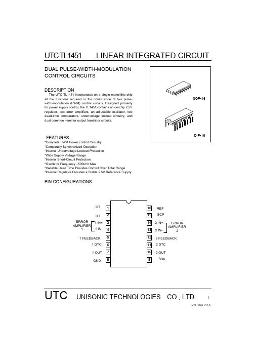
UTC TL1451LINEAR INTEGRATED CIRCUITUTC UNISONIC TECHNOLOGIES CO., LTD.1QW-R103-011,ADUAL PULSE-WIDTH-MODULATION CONTROL CIRCUITSDESCRIPTIONThe UTC TL1451 incorporates on a single monolithic chipall the functions required in the construction of two pulse-width-modulation (PWM) control circuits. Designed primarily for power supply control, the TL1451 contains an on-chip 2.5V regulator, two error amplifiers, an adjustable oscillator, two dead-time comparators, undervoltage lockout circuitry, and dual common –emitter output transistor circuits.FEATURES*Complete PWM Power control Circuitry *Completely Synchronized Operation*Internal Undervoltage Lockout Protection *Wide Supply Voltage Range *Internal Short-Circuit Protection *Oscillator Frequency …500kHz Max*Variable Dead Time Provides Control Over Total Range *Internal Regulator Provides a Stable 2.5V Reference SupplyPIN CONFIGURATIONSCT RT1 IN+1 IN-1 FEEDBACK1 DTC 1 OUT GNDVcc2 OUT 2 DTC 2 IN-SCPREF 2 IN+2 FEEDBACK ERROR AMPLIFIER1ERROR AMPLIFIER212345678910111213141516UTC TL1451LINEAR INTEGRATED CIRCUIT BLOCK DIAGRAMUTC UNISONIC TECHNOLOGIES CO., LTD.2QW-R103-011,AUTC TL1451LINEAR INTEGRATED CIRCUITUTC UNISONIC TECHNOLOGIES CO., LTD.3QW-R103-011,AABSOLUTE MAXIMUM RATINGS (Unless otherwise noted all is over operating free air temperaturerange)PARAMETERSYMBOL VALUE UNIT Supply VoltageV CC 51V Amplifier Input Voltage V I 20V Collector Output Voltage V O 51V Collector Output CurrentI O21mA Power Dissipation : TA ≤25°C DIP SOP1000500mWOperating free-air Temperature Range T A -20 TO 85°C Storage Temperature RangeTstg -65 TO 150°C Lead Temperature 1.6mm from Case for 10Sec.Tcase 260°CRECOMMENDED OPERATING CONDITIONSPARAMETERSYMBOLVALUEUNIT MINMAX Supply VoltageVcc 3.650V Amplifier Input Voltage Vi 1.051.45V Collector Output VoltageVo 50V Collector Output Current(each Transistor)Io 20mA Current into Feedback Terminal 45µA Feedback Resistor R F 100k ΩTiming Capacitor C T 15015000pF Timing Resistor R T 5.1100k ΩOscillator frequency1500kHz Operating Free-Air TemperatureT A-2085°CELECTRICAL CHARACTERISTICS(Over recommended operating free-air temperature range,V CC =6V,f=200kHz,TA=25°C ,Unless otherwise specified)PARAMETER TEST CONDITIONS MIN TYP MAX UNITReference SectionOutput VoltageIo=1mA2.42.5 2.6VOutput Voltage Change with Temperature T A =-20°C to 25°C T A =25°C to 85°C -0.1-0.2±1%±1%Input Voltage Regulation Vcc=3.6V to 40V 212.5mV Output Voltage Regulation Io=0.1mA to 1mA17.5mV Short-Circuit Output CurrentVo=031030mA Undervoltage Lockout Section Upper Threshold Voltage (Vcc) 2.72V Lower Threshold Voltage (Vcc) 2.6V Hysteresis (Vcc)80120mV Reset Threshold voltage (Vcc)Io(ref)=0.1mA, T A =25°C1.5 1.9V Short-Circuit Protection Control Section Input Threshold Voltage(SCP)TA=25°C0.650.70.75VUTC TL1451LINEAR INTEGRATED CIRCUITUTC UNISONIC TECHNOLOGIES CO., LTD.4QW-R103-011,APARAMETERTEST CONDITIONS MIN TYP MAX UNIT Standby Voltage(SCP)No pullup 140185230mV Latched Input Voltage (SCP)No pullup 60120mV Input (source) CurrentVI=0.7V,T A =25°C-10-15-20µA Comparator Threshold Voltage (FEEDBACK)1.18V Oscillator SectionFrequencyC T =330pF, R T =10k Ω200kHzStandard deviation of frequency C T =330pF, R T =10k Ω10%Frequency Change with VoltageVcc=3.6V to 40V 1%Frequency Change with TemperatureTA=-20°C to 25°C TA=25°C to 85°C-0.4%-0.2%±2%±2%Dead-Time Control SectionInput bias Current (DTC)1µA Latch mode (source) Current (DTC)TA=25°C -80-145µA Latched Input Voltage (DTC)Io=40µA 2.3V Input threshold Voltage at f=10kHz (DTC)Zero duty cycle Maximum duty cycle 1.22.051.452.25VError-Amplifier Section Input Offset Voltage Vo (FEEDBACK)=1.25V ±6mV Input Offset Current Vo (FEEDBACK)=1.25V ±100nA Input Bias currentVo (FEEDBACK)=1.25V160500nA Common-Mode Input Voltage Range Vcc=3.6V to 40V1.05 to 1.45V Open-loop Voltage Amplification R F =200k Ω7080dB Unity-gain Bandwidth1.5MHz Common-mode Rejection Ratio 6080dB Positive Output Voltage Swing Vref-0.1VNegative Output Voltage Swing 1V Output (sink) Current (FEEDBACK)V ID =-0.1V,Vo=1.25V 0.5 1.6mA Output (source) Current (FEEDBACK)V ID =-0.1V,Vo=1.25V-45-70µA Output SectionCollector off-state Current Vo=50V 10µA Output Saturation Voltage Io=10mA 1.22V Short-Circuit Output CurrentVo=6V 90mA PWM Comparator Section Input Threshold Voltage at f=10kHz (FEEDBACK)Zero duty cycle Maximum duty cycle1.22.051.45 2.25VTOTAL DEVICEStandby Supply Current Off-state 1.3 1.8mA Average Supply CurrentR T =10k Ω1.72.4mAUTC TL1451LINEAR INTEGRATED CIRCUITUTC UNISONIC TECHNOLOGIES CO., LTD.5QW-R103-011,ATEST CIRCUITTIMING DIAGRAM。
- 1、下载文档前请自行甄别文档内容的完整性,平台不提供额外的编辑、内容补充、找答案等附加服务。
- 2、"仅部分预览"的文档,不可在线预览部分如存在完整性等问题,可反馈申请退款(可完整预览的文档不适用该条件!)。
- 3、如文档侵犯您的权益,请联系客服反馈,我们会尽快为您处理(人工客服工作时间:9:00-18:30)。
VALUE 15V (or +-7.5)
15 -0.3 ~ +15
UNIT V V V
Power Dissipation Operating Temperature Storage Temperature
市 PD Topr Tstg
300 -20 to +75 -40 to +125
mW °C °C
Ib
MIN TYP MAX UNIT
2
5
mV
5
100
nA
100 500
nA
Large Signal Voltage Gain Input Common Voltage Range
Av VICM
RL=2KΩ
88 100
dB
V+-2
V
Maximum Output Voltage Swing VOM1
RL>=2kΩ,V+=5V
Q14
技Q15 Q20
C2
Q27
R7
V-
科OUTPUT
安
达 ABSOLUTE MAXIMUM RATINGS(Ta=25°C )
PARAMETER
SYMBOL
Supply Voltage Differential Input Voltage Input Voltage
众V+(V+/V-) VID VI
司 公 限 有 技 科 安 达 众 市 圳 深
电话:(0755)27858667 27858661 传真:(0755)27858707 4
UTC 3414
LINEAR INTEGRATED CIRCUIT
司 公 限 有 技 科 安 达 众 市 圳 深
电话:(0755)27858667 27858661 传真:(0755)27858707 5
UTC 3414
LINEAR INTEGRATED CIRCUIT
SINGLE-SUPPLY DUAL HIGH CURRENT OPERATIONAL AMPLIFIER
DESCRIPTION
SOP-8
The UTC 3414 integrated circuit is a high gain, high output current, high output voltage swing dual operational amplifier capable of driving 70mA.
3.5
V
1
电话:(0755)27858667 27858661 传真:(0755)27858707 2
UTC 3414
LINEAR INTEGRATED CIRCUIT
PARAMETER
SYMBOL
TEST CONDITIONS
MIN TYP MAX UNIT
Maximum Output Voltage Swing VOM2
Io=70mA,V+=5V
3.2
V
2
Common Mode Rejection Ratio CMR
80
90
dB
Supply Voltage Rejection Ratio SVR
80
90
dB
Operating Current
Icc
RL=∝
3
4
5
mA
Slew Rate
SR
1.0
V/µs
Unity Gain Bandwidth
司
FEATURES
*Single Supply *Operating Voltage *High Output Current *Slew Rate *Bipolar Technology
(+3V~+15V) (70mA) (1.0V/µs typ.)
公DIP-8
限
有
TSSOP-8
PIN CONFIGURATIONS
圳 ELECTRICAL CHARACTERISTICS(Ta=25°C, V+=8.6V)
深PARAMETER
Input Offset Voltage Input Offset Current
SYMBOL VIO IIO
TEST CONDITIONS Rs=0Ω
Input Bias Current
技
科
安
达 OUT 1 1
众 IN 1(-) 2
A
8
V+
7 OUT 2
市IN 1(+) 3
B
6 IN 2(-)
圳 GND 4
5 INБайду номын сангаас2(+)
深
电话:(0755)27858667 27858661 传真:(0755)27858707 1
UTC 3414
LINEAR INTEGRATED CIRCUIT
BLOCK DIAGRAM
V+
Q22-A
Q21
Q22-B
Q23 Q24
Q31 Q25
Q22-D
-INPUT +INPUT
Q3 Q4
Q1
Q7 Q9
Q22-C
Q5 Q6
C1 Q2
Q8
Q10
Q11
Q16
司 Q12 R2
Q18 Q30 Q17
公 R3
Q13 R4
有限 R1
R5 Q18 Q26
Q33 R6
Q29 Q32 Q34
GB
Operating Voltage Range
V+
司 1.3
MHz
15
V
公
限
有
技
科
安
达
众
市
圳
深
电话:(0755)27858667 27858661 传真:(0755)27858707 3
UTC 3414
LINEAR INTEGRATED CIRCUIT
TYPICAL CHARACTERISTICS
UTC 3414
LINEAR INTEGRATED CIRCUIT
司 公 限 有 技 科 安 达 众 市 圳 深
UTC assumes no responsibility for equipment failures that result from using products at values that exceed, even momentarily, rated values (such as maximum ratings, operating condition ranges, or other parameters) listed in products specifications of any and all UTC products described or contained herein. UTC products are not designed for use in life support appliances, devices or systems where malfunction of these products can be reasonably expected to result in personal injury. Reproduction in whole or in part is prohibited without the prior written consent of the copyright owner. The information presented in this document does not form part of any quotation or contract, is believed to be accurate and reliable and may be changed without notice.
电话:(0755)27858667 27858661 传真:(0755)27858707 6