Q62702-A1047中文资料
Q62702-F1062中文资料
Gma
IC = 15 mA, VCE = 8 V, ZS = ZSopt ZL = ZLopt f = 900 MHz f = 1.8 GHz
Transducer gain |S21e|2 11.5 6 13.5 8 -
IC = 15 mA, VCE = 8 V, ZS =ZL= 50 Ω f = 900 MHz f = 1.8 GHz
Package Equivalent Circuit: LBI = LBO = LEI = LEO = LCI = LCO = CBE = CCB = CCE = 84 165 0.85 0.51 0.69 0.61 0 0.49 nH nH nH nH nH nH fF fF fF
Valid up to 6 GHz For examples and ready to use parameters please contact your local Siemens distributor or sales office to obtain a Siemens CD-ROM or see Internet: http://www.siemens.de/Semiconductor/products/35/35.htm
0.90551 12.196 1.2703 0.79584 0.66749 0.32167 0.21451 922.07 0.3 0.75 1.11 300
fA mA Ω V fF V eV K
0.016123 A 0.019729 A
0.024709 fA
0.013277 mA
All parameters are ready to use, no scalling is necessary. Extracted on behalf of SIEMENS Small Signal Semiconductors by: Institut für Mobil-und Satellitenfunktechnik (IMST) © 1996 SIEMENS AG
BFP196中文资料

Semiconductor Group
3
Dec-13-1996
元器件交易网
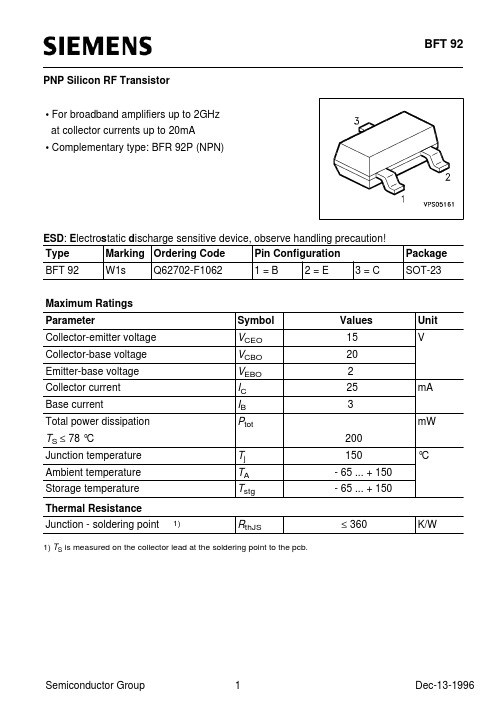
BFP 196
SPICE Parameters (Gummel-Poon Model, Berkeley-SPICE 2G.6 Syntax) : Transistor Chip Data IS = 1.7264 fA VAF = NE = VAR = NC = RBM = CJE = TF = ITF = VJC = TR = MJS = XTI = 20 1.1766 3.8128 0.88299 1 13.325 23.994 1.9775 0.73057 2.2413 0 3 V V Ω fF ps mA V ns -
F = 1.5 dB at 900MHz
ESD: Electrostatic discharge sensitive device, observe handling precaution! Type Marking Ordering Code Pin Configuration BFP 196 RIs Q62702-F1320 1=C 2=E 3=B 4=E
BFP 196
Electrical Characteristics at TA = 25°C, unless otherwise specified. Parameter Symbol min. AC Characteristics Transition frequency Values typ. max. Unit
(3rd order, Output, ZS=ZL=50Ω)
f = Parameter
18
VCE = Parameter, f = 900MHz
BC846PN中文资料
RthJS
10 1
10 -1 -6 10
10
-5
10
-4
10
-3
10
-2
s
10
0
10 0 -6 10
10
-5
10
-4
10
-3
10
-2
s
10
0
tp
tp
Semiconductor Group Semiconductor Group
44
Hale Waihona Puke Sep-07-1998 1998-11-01
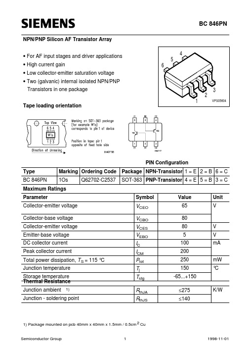
BC 846PN
Collector-base capacität CCB = f (V CBO) Emitter-base capacität CEB = f (VEBO)
0.5
h 22e
10 -1
0
10 -1
5
10 0
mA
10 1
0
10
20
V
30
ΙC
Semiconductor Group Semiconductor Group 66
VCE
Sep-07-1998 1998-11-01
Unit
fT Ccb Ceb h11e h12e h21e h22e
-
MHz pF
I C = 20 mA, VCE = 5 V, f = 100 MHz
Collector-base capacitance
VCB = 10 V, f = 1 MHz
Emitter-base capacitance
VEB = 0.5 V, f = 1 MHz
DC current gain 1)
I C = 10 µA, VCE = 5 V I C = 2 mA, V CE = 5 V
SFH757中文资料
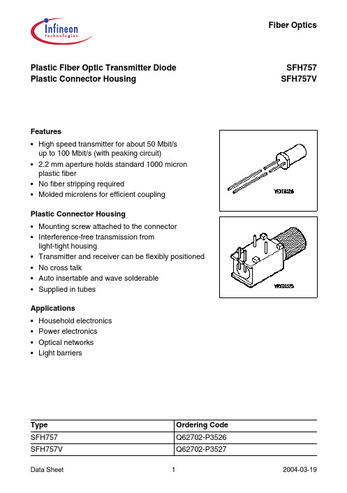
Type Ordering Code SFH757Q62702-P3526SFH757VQ62702-P3527Plastic Fiber Optic Transmitter Diode Plastic Connector HousingSFH757SFH757VFiber OpticsFeatures•High speed transmitter for about 50Mbit/s up to 100Mbit/s (with peaking circuit)• 2.2mm aperture holds standard 1000 micron plastic fiber•No fiber stripping required•Molded microlens for efficient coupling Plastic Connector Housing•Mounting screw attached to the connector •Interference-free transmission from light-tight housing•Transmitter and receiver can be flexibly positioned •No cross talk•Auto insertable and wave solderable •Supplied in tubes Applications •Household electronics •Power electronics •Optical networks •LightbarriersTechnical DataAbsolute Maximum RatingsParameter Symbol Limit Values Unitmin.max. Operating Temperature Range T OP–40+80°C Storage Temperature Range T STG–40+100°C Junction Temperature T J100°CSoldering Temperature(2mm from case bottom, t≤ 5s)TS260°CReverse Voltage V R3V Forward Current I F50mA Surge Current (t≤ 10µs, D=0)I FSM1A Power Dissipation P tot120mW Thermal Resistance, Junction/Air R thJA450K/WCharacteristics (T A = 25°C)Parameter Symbol Value Unit Peak WavelengthλPeak650nm Spectral Bandwidth∆λ25nmSwitching Times (R L = 50Ω, I F = 50mA) 10% …90%90% … 10%tRtF15 (< 17)18 (< 20)nsCapacitance (f = 1MHz, V R = 0V)C O30pF Forward Voltage (I F = 50mA)V F 2.1 (≤ 2.8)VOutput Power Coupled into Plastic Fiber (I F = 10mA)1)ΦIN150(≥ 100)µWTemperature Coefficient ΦIN TCΦ–0.4%/K Temperature Coefficient V F TC V–3mV/K Temperature Coefficient λPeak TCλ0.16nm/K1)The output power coupled into plastic fiber is measured with a large area detector at the end of a short lengthof fiber (about 30cm). This value must not be used for calculating the power budget for a fiber optic system with a long fiber because the numerical aperture of plastic fibers decreases on the first meters. Therefore the fiber seems to have a higher attenuation over the first few meters compared with the specified value.Relative Spectral Emission I rel = f (λ)Relative Output Power I e /I e(50 mA) = f (I F ) single pulse, duration = 20 µsForward Current I F = f (V F ) single pulse, duration = 20 µsMaximum Permissible Forward Current IF = f (T A ), R thJA= 450 K/WPermissible Pulse Handling CapabilityI F = f(t P), duty cycle D = parameter,TA= 25°CSFH757SFH757VPackage Outlines Package OutlinesFigure1Figure2Edition 2004-03-19Published by Infineon Technologies AG,St.-Martin-Strasse 53,81669 München, Germany© Infineon Technologies AG 2004.All Rights Reserved.Attention please!The information herein is given to describe certain components and shall not be considered as a guarantee of characteristics.Terms of delivery and rights to technical change reserved.We hereby disclaim any and all warranties, including but not limited to warranties of non-infringement, regarding circuits, descriptions and charts stated rmationFor further information on technology, delivery terms and conditions and prices please contact your nearest Infineon Technologies Office ( ).WarningsDue to technical requirements components may contain dangerous substances. For information on the types in question please contact your nearest Infineon Technologies Office.Infineon Technologies Components may only be used in life-support devices or systems with the express written approval of Infineon Technologies, if a failure of such components can reasonably be expected to cause the failure of that life-support device or system, or to affect the safety or effectiveness of that device or system. Life support devices or systems are intended to be implanted in the human body, or to support and/or maintain and sustain and/or protect human life. If they fail, it is reasonable to assume that the health of the user or other persons may SFH757SFH757V Revision History:2004-03-19DS1Previous Version:2002-03-14。
Q62702-G0067中文资料
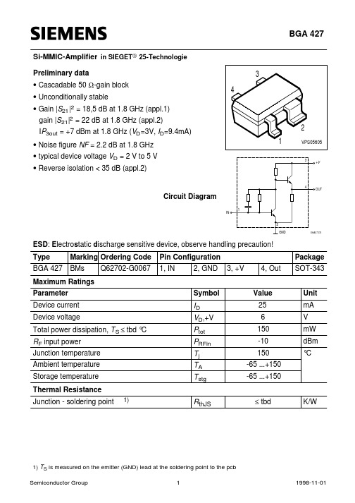
in SIEGET ® 25-Technologie Si-MMIC-Amplifier VPS056054213Preliminary data• Cascadable 50 Ω-gain block • Unconditionally stable• Gain |S 21|2 = 18,5 dB at 1.8 GHz (appl.1) gain |S 21|2 = 22 dB at 1.8 GHz (appl.2) I P 3out = +7 dBm at 1.8 GHz (V D =3V, I D =9.4mA)• Noise figure NF = 2.2 dB at 1.8 GHz • typical device voltage V D = 2 V to 5 V • Reverse isolation < 35 dB (appl.2)VCircuit DiagramESD : E lectro s tatic d ischarge sensitive device, observe handling precaution!Type Marking Ordering Code PackagePin Configuration Q62702-G00671, INBGA 4272, GND 3, +V4, Out SOT-343BMsMaximum Ratings SymbolValue ParameterUnit Device current I D mA 25Device voltage6V V D ,+V P tot 150mW Total power dissipation, T S ≤ tbd °CdBm R F input power P RFin -10Junction temperature T j 150°CAmbient temperature -65 ...+150T A Storage temperatureT stg-65 ...+150Thermal Resistance ≤ tbdK/WJunction - soldering point 1)R thJS1) T S is measured on the emitter (GND) lead at the soldering point to the pcbElectrical Characteristics at T A = 25 °C, unless otherwise specified.Parameter Symbol UnitValuestyp.max.min.AC characteristics V D = 3 V, Z o = 50W, Testfixture Appl..1|S 21|2 - - -Insertion power gain f = 0.1 GHz f = 1 GHz f = 1.8 GHz 27 22 28.5 - - -dBReverse isolation f = 1.8 GHz S12-22-Noise figure f = 0.1 GHz f = 1 GHz f = 1.8 GHz- - - - - - 1.9 2 2.2NFIntercept point at the output f = 1.8 GHzIP 3out -+ 7 -dBm Return loss input f = 1.8 GHzRL in ->12-dB Return loss output f = 1.8 GHzRL out->9-Typical configurationAppl.2Appl.1EHA07379100 pF100 pF1 nFRF OUTRF INGND+VBGA 427100 pFNote: 1) Large-value capacitors should be connected from pin 3 to ground right at the device to provide a low impedance path! (appl.1)2) The use of plated through holes right at pin 2 is essential for pc-board-applications. Thin boards are recommended to minimize the parasitic inductance to ground!S-Parameters at T A = 25 °C, (Testfixture, Appl.1)fS 11S 21S 12S 22GHzMAGANGMAGANGMAGANGMAGANG-0.0022 0.0046 0.0104 0.0169 0.0194 0.0225 0.0385 0.0479 0.0517 0.0549 0.0709 0.089250.7 71.8 83.8 94.8 97.3 98.3 99.7 99.3 98.9 98.8 97.1 96.90.1 0.2 0.5 0.8 0.9 1 1.5 1.8 1.9 2 2.5 3-38.3 -16 -20.8 -56.9 -69.1 -80.6 -133.5 -156.1 -162.8 -167.7 172.8 153.3164.9 158.9 135.2 115.4 109.4 104 84.9 77 74.7 72.3 63 5524.821 24.606 22.236 18.258 17.152 15.786 10.923 9.029 8.486 8.015 6.2595.1030.1382 0.1179 0.1697 0.1824 0.1782 0.176 0.1827 0.1969 0.2021 0.2116 0.2437 0.2580.6435 0.6278 0.54 0.4453 0.4326 0.4129 0.3852 0.3917 0.3946 0.3991 0.4202 0.4477174.8 166.9 147.3 140.2 139.4 138.1 139.6 139.3 138.8 138.3 134.6 131Spice-model BGA 427OUTT1T501T2T501R 114.5k ΩR 2280ΩR 3 2.4k ΩR 4170ΩC 1 2.3pF C P10.2pF 0.2pF C P2C P30.6pFC P40.1pF C P50.1pF C’-E’-diode T1Transistor Chip Data T1 (Berkley-SPICE 2G.6 Syntax) :IS =0.21024aA V 39.251VAF =NE = 1.7763-V VAR =34.368NC = 1.3152-ΩRBM = 1.3491CJE = 3.7265fF ps 4.5899TF =ITF = 1.3364mA V 0.99532VJC =TR = 1.4935ns -MJS =0XTI =3-NF =1.0405-ISE =fA 15.7610.96647-NR =ISC =0.037223fA 0.21215mA IRB =RC =Ω0.126910.37747-MJE =VTF =V 0.1976296.941fF CJC =XCJC =0.08161-0.75V VJS =EG = 1.11eV 300KTNOMBF =83.23-A 0.16493IKF =BR =10.526-A IKR =0.25052RB =15ΩRE = 1.9289VJE =0.70367V -XTF =0.3641PTF =0deg -0.48652MJC =CJS =0fF -XTB =0FC =0.99469-C’-E’-Diode Data (Berkley-SPICE 2G.6 Syntax) :RS =20ΩIS =2fA -1.02N =All parameters are ready to use, no scalling is necessaryPackage Equivalent Circuit:Extracted on behalf of SIEMENS Small Signal Semiconductors by Institut für Mobil-und Satellitentechnik (IMST)© 1996 SIEMENS AGFor examples and ready to use parameters please contact your local Siemens distributor or sales o ffice to obtain a Siemens CD-ROM or see Internet: http://www.siemens.de/Semiconductor/products/35/35.htmInsertion power gain |S 21|2 = f (f )V D , I D = parameter1|S 21|2Noise figure NF = f (f )V D ,I D= parameter1NFIntercept point at the outputIP 3out = f (f )V D,I D = parameter1dBmI P 3o u t。
Q62702-G44资料
Siemens Aktiengesellschaft
pg. 1/7
17.09.96 HL EH PD21/Gü
元器件交易网
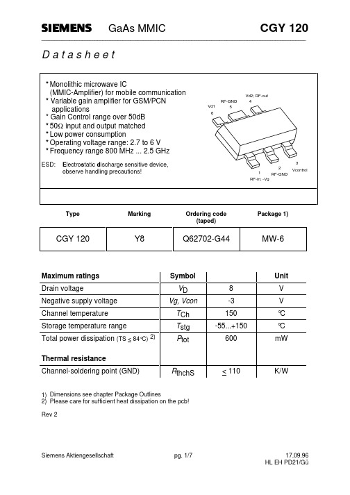
GaAs MMIC
Electrical characteristics TA = 25°C f = 900 MHz Characteristics Power Gain Vd=3V; I=45mA; Vcon=2V Vd=5V; I=70mA; Vcon=2V Input return loss Vd=3V; I=45mA; Vcon=2V Vd=5V; I=70mA; Vcon=2V Output return loss Vd=3V; I=45mA; Vcon=2V Vd=5V; I=70mA; Vcon=2V Gain Control Range
C1 , C2 Siemens B37490-K5120-J62 R1 Siemens B54102-A1471-J60 L1 Coilcraft 0805CS-270XMBC C4 Siemens B37940-K5220-J62 R2 Siemens B53102-A1511-J60 L2 Coilcraft 0805CS-220XMBC C3 , C5 Siemens B37940-K5681-J62 For optimized device performance, Vg has to be adapted (Vg ≈ -1V...0V) to I ≈ 45mA at Vd-supply under condition Vcontrol=+2V.
dG P1dB
1dBm gain compression Vd=3V; I=45mA; Vcon=2V Vd=5V; I=70mA; Vcon=2V
BAS125-04W中文资料

Electrical Characteristics at TA=25°C, unless otherwise specified Parameter Symbol min. DC characteristics Reverse current Values typ. max. Unit
IR
385 530 800 150 200
Semiconductor Group
5
Dec-20-1996
BAS 125-04W... (IF per diode)
100 mA
IF
80
TS
70 60 50 40 30 20 10 0 0 20 40 60 80 100 120 °C 150 TA ,TS
TA
Permissible Pulse Load RTHJS = f(tp)
BAS 125-04W...
BAS 125W
100 mA
IF
80 70 60 50 40 30 20 10 0 0 20 40 60 80 100
TS
TA
120 °C 150 TA ,TS
Permissible Pulse Load RTHJS = f(tp)
BAS 125W
10 3
Permissible Pulse Load IFmax/IFDC = f(tp)
nA
VR = 20 V VR = 25 V
Forward voltage
VF
400 650 900
mV
IF = 1 mA IF = 10 mA IF = 35 mA
AC Characteristics Diode capacitance
CT
16 1.1
SFH214中文资料

Neu:Silizium-PIN-Fotodiode mit sehr kurzer Schaltzeit New:Silicon PIN Photodiode with Very ShortSwitching TimeTyp Type Bestellnummer Ordering CodeSFH 214Q62702-P922SFH 214 FAQ62702-P1672SFH 214SFH 214 FAMaße in mm, wenn nicht anders angegeben/Dimensions in mm, unless otherwise specified.f e o f 6652f e o 06652Wesentliche Merkmaleq Speziell geeignet für Anwendungen im Bereich von 400 nm bis 1100 nm(SFH 214) und bei 880 nm (SFH 214 FA)q Kurze Schaltzeit (typ. 5 ns)q 5 mm-Plastikbauform im LED-Gehäuse q Auch gegurtet lieferbarAnwendungenq Industrieelektronikq “Messen/Steuern/Regeln”q Schnelle Lichtschranken für Gleich- und Wechsellichtbetrieb q LWL Featuresq Especially suitable for applications from 400 nm to 1100 nm (SFH 214) and of 880 nm (SFH 214 FA)q Short switching time (typ. 5 ns)q 5 mm LED plastic package q Also available on tapeApplicationsq Industrial electronicsq For control and drive circuits q Photointerruptersq Fiber optic transmission systemsGrenzwerteMaximum Ratings Bezeichnung DescriptionSymbol SymbolWert Value Einheit Unit Betriebs- und LagertemperaturOperating and storage temperature range T op ;T stg – 55...+ 100°C Löttemperatur (Lötstelle 2 mm vom Gehäuse entfernt bei Lötzeit t ≤ 3 s)Soldering temperature in 2 mm distance from case bottom (t ≤ 3 s)T S300°CSperrspannung Reverse voltage V R 50V VerlustleistungTotal power dissipationP tot100mWKennwerte (T A = 25°C)Characteristics Bezeichnung DescriptionSymbol SymbolWert ValueEinheit UnitSFH 214SFH 214 FAFotoempfindlichkeit Spectral sensitivityV R = 5 V, Normlicht/standard light A,T = 2856 K,V R = 5 V,λ = 870 nm,E e = 1 mW/cm 2S S45 (≥ 30)––25 (≥ 20)nA/Ix µA Wellenlänge der max. Fotoempfindlichkeit Wavelength of max. sensitivityλS max 850900nm Spektraler Bereich der Fotoempfindlichkeit S = 10 % von S maxSpectral range of sensitivity S = 10 % of S maxλ400...1100750 (1100)nmBestrahlungsempfindliche Fläche Radiant sensitive areaA 11mm 2Abmessung der bestrahlungsempfindlichen FlächeDimensions of radiant sensitive area L ×B L ×W 1×11×1mm ×mmAbstand Chipoberfläche zu Gehäuseober-flächeDistance chip front to case surfaceH3.4...4.0 3.4...4.0mmHalbwinkel Half angleϕ±40±40Grad deg.Dunkelstrom,V R = 20 V Dark currentI R 1 (≤ 5) 1 (≤ 5)nA Spektrale Fotoempfindlichkeit,λ = 850 nm Spectral sensitivityS λ0.620.59A/W Quantenausbeute,λ = 850 nm Quantum yieldη0.890.86Electrons Photon Leerlaufspannung Open-circuit voltageE v = 1000 Ix, Normlicht/standard light A,T = 2856 KE e = 0.5 mW/cm 2,λ = 870 nmV O V O380 (≥ 300)––340 (≥ 290)mV mVKurzschlußstrom Short-circuit currentE v = 1000 Ix, Normlicht/standard light A,T = 2856 KE e = 0.5 mW/cm 2,λ = 870 nmI SC I SC 42––12µA µA Anstiegs- und Abfallzeit des Fotostromes Rise and fall time of the photocurrentR L = 50Ω;V R = 20 V;λ = 850 nm;I p = 800µA t r ,t f55nsDurchlaßspannung,I F = 80 mA,E = 0Forward voltageV F 1.3 1.3V Kapazität,V R = 0 V,f = 1 MHz,E = 0CapacitanceC 01111pF Temperaturkoeffizient von V O Temperature coefficient of V O TC V – 2.6– 2.6mV/K Temperaturkoeffizient von I SC Temperature coefficient of I SC Normlicht/standard light A λ = 870 nmTC I0.18––0.2%/KRauschäquivalente Strahlungsleistung Noise equivalent power V R = 10 V,λ = 850 nmNEP2.9×10– 14 2.9×10– 14W √Hz Nachweisgrenze,V R = 20 V,λ = 850 nm Detection limitD*3.5×10¹² 3.5×1012cm ·√Hz WKennwerte (T A = 25°C)Characteristics (cont’d)Bezeichnung Description Symbol SymbolWert ValueEinheit UnitSFH 214SFH 214 FARelative spectral sensitivity SFH 214S rel =f (λ)Photocurrent I P =f (E e ),V R = 5 V Open-circuit voltage V O =f (E e )SFH 214 FARelative spectral sensitivity SFH 214 FA S rel =f (λ)Total power dissipation P tot =f (T A)Photocurrent I P =f (E v ),V R = 5 V Open-circuit voltage V O =f (E v )SFH 214Dark current I R =f (V R ),E= 0Directional characteristics S rel =f (ϕ)。