UDM40LSESXR5LTX中文资料
LM4040_05中文资料
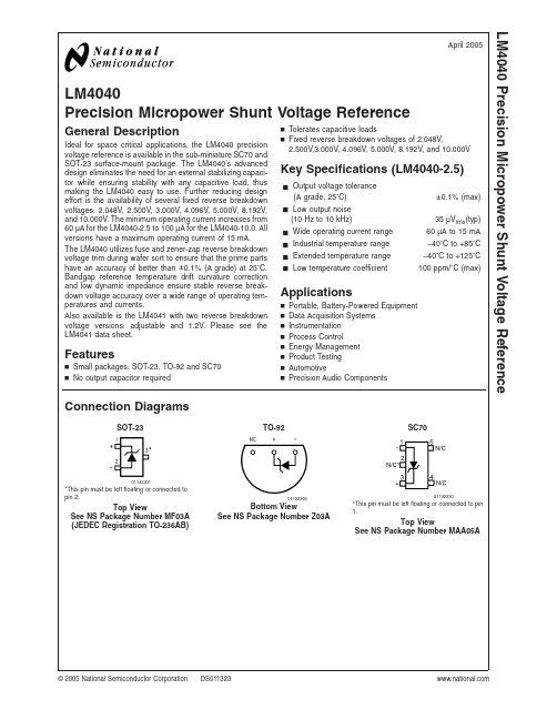
LM4040Precision Micropower Shunt Voltage ReferenceGeneral DescriptionIdeal for space critical applications,the LM4040precision voltage reference is available in the sub-miniature SC70and SOT-23surface-mount package.The LM4040’s advanced design eliminates the need for an external stabilizing capaci-tor while ensuring stability with any capacitive load,thus making the LM4040easy to use.Further reducing design effort is the availability of several fixed reverse breakdown voltages:2.048V,2.500V,3.000V,4.096V,5.000V,8.192V,and 10.000V.The minimum operating current increases from 60µA for the LM4040-2.5to 100µA for the LM4040-10.0.All versions have a maximum operating current of 15mA.The LM4040utilizes fuse and zener-zap reverse breakdown voltage trim during wafer sort to ensure that the prime parts have an accuracy of better than ±0.1%(A grade)at 25˚C.Bandgap reference temperature drift curvature correction and low dynamic impedance ensure stable reverse break-down voltage accuracy over a wide range of operating tem-peratures and currents.Also available is the LM4041with two reverse breakdown voltage versions:adjustable and 1.2V.Please see the LM4041data sheet.Featuresn Small packages:SOT-23,TO-92and SC70n No output capacitor requiredn Tolerates capacitive loadsn Fixed reverse breakdown voltages of 2.048V,2.500V,3.000V,4.096V,5.000V,8.192V,and 10.000VKey Specifications (LM4040-2.5)j Output voltage tolerance(A grade,25˚C)±0.1%(max)j Low output noise(10Hz to 10kHz)35µV rms (typ)j Wide operating current range 60µA to 15mA j Industrial temperature range −40˚C to +85˚C j Extended temperature range −40˚C to +125˚C j Low temperature coefficient100ppm/˚C (max)Applicationsn Portable,Battery-Powered Equipment n Data Acquisition Systems n Instrumentation n Process Controln Energy Management n Product Testing n AutomotivenPrecision Audio ComponentsConnection DiagramsSOT-23TO-92SC7001132301*This pin must be left floating or connected to pin 2.Top ViewSee NS Package Number MF03A (JEDEC Registration TO-236AB)01132303Bottom ViewSee NS Package Number Z03A01132330*This pin must be left floating or connected to pin1.Top ViewSee NS Package Number MAA05AApril 2005LM4040Precision Micropower Shunt Voltage Reference©2005National Semiconductor Corporation Ordering InformationIndustrial Temperature Range (−40˚C to +85˚C)Reverse Breakdown Voltage Tolerance at 25˚C and Average Reverse Breakdown Voltage Temperature CoefficientPackageNS Package NumberM3(SOT-23)M7(SC70)Z (TO-92)Supplied as 1000Units Tape andReelSupplied as 3000Units tape andReelSupplied as 1000Units Tape andReelSupplied as 3000Units Tape andReel±0.1%,100ppm/˚C max (A grade)LM4040AIM3-2.0LM4040AIM3-2.5LM4040AIM3-3.0LM4040AIM3-4.1LM4040AIM3-5.0LM4040AIM3-8.2LM4040AIM3-10.0LM4040AIM3X-2.0LM4040AIM3X-2.5LM4040AIM3X-3.0LM4040AIM3X-4.1LM4040AIM3X-5.0LM4040AIM3X-8.2LM4040AIM3X-10.0LM4040AIZ-2.0LM4040AIZ-2.5LM4040AIZ-3.0LM4040AIZ-4.1LM4040AIZ-5.0LM4040AIZ-8.2LM4040AIZ-10.0MF03A,Z03A±0.2%,100ppm/˚C max (B grade)LM4040BIM3-2.0LM4040BIM3-2.5LM4040BIM3-3.0LM4040BIM3-4.1LM4040BIM3-5.0LM4040BIM3-8.2LM4040BIM3-10.0LM4040BIM3X-2.0LM4040BIM3X-2.5LM4040BIM3X-3.0LM4040BIM3X-4.1LM4040BIM3X-5.0LM4040BIM3X-8.2LM4040BIM3X-10.0LM4040BIM7-2.0LM4040BIM7-2.5LM4040BIM7-3.0LM4040BIM7-4.1LM4040BIM7-5.0LM4040BIM7X-2.0LM4040BIM7X-2.5LM4040BIM7X-3.0LM4040BIM7X-4.1LM4040BIM7X-5.0LM4040BIZ-2.0LM4040BIZ-2.5LM4040BIZ-3.0LM4040BIZ-4.1LM4040BIZ-5.0LM4040BIZ-8.2LM4040BIZ-10.0MF03A,Z03A,MAA05A ±0.5%,100ppm/˚C max (C grade)LM4040CIM3-2.0LM4040CIM3-2.5LM4040CIM3-3.0LM4040CIM3-4.1LM4040CIM3-5.0LM4040CIM3-8.2LM4040CIM3-10.0LM4040CIM3X-2.0LM4040CIM3X-2.5LM4040CIM3X-3.0LM4040CIM3X-4.1LM4040CIM3X-5.0LM4040CIM3X-8.2LM4040CIM3X-10.0LM4040CIM7-2.0LM4040CIM7-2.5LM4040CIM7-3.0LM4040CIM7-4.1LM4040CIM7-5.0LM4040CIM7X-2.0LM4040CIM7X-2.5LM4040CIM7X-3.0LM4040CIM7X-4.1LM4040CIM7X-5.0LM4040CIZ-2.0LM4040CIZ-2.5LM4040CIZ-3.0LM4040CIZ-4.1LM4040CIZ-5.0LM4040CIZ-8.2LM4040CIZ-10.0MF03A,Z03A,MAA05A ±1.0%,150ppm/˚C max (D grade)LM4040DIM3-2.0LM4040DIM3-2.5LM4040DIM3-3.0LM4040DIM3-4.1LM4040DIM3-5.0LM4040DIM3-8.2LM4040DIM3-10.0LM4040DIM3X-2.0LM4040DIM3X-2.5LM4040DIM3X-3.0LM4040DIM3X-4.1LM4040DIM3X-5.0LM4040DIM3X-8.2LM4040DIM3X-10.0LM4040DIM7-2.0LM4040DIM7-2.5LM4040DIM7-3.0LM4040DIM7-4.1LM4040DIM7-5.0LM4040DIM7X-2.0LM4040DIM7X-2.5LM4040DIM7X-3.0LM4040DIM7X-4.1LM4040DIM7X-5.0LM4040DIZ-2.0LM4040DIZ-2.5LM4040DIZ-3.0LM4040DIZ-4.1LM4040DIZ-5.0LM4040DIZ-8.2LM4040DIZ-10.0MF03A,Z03A,MAA05A ±2.0%,150ppm/˚C max (E grade)LM4040EIM3-2.0LM4040EIM3-2.5LM4040EIM3-3.0LM4040EIM3X-2.0LM4040EIM3X-2.5LM4040EIM3X-3.0LM4040EIM7-2.0LM4040EIM7-2.5LM4040EIM7-3.0LM4040EIM7X-2.0LM4040EIM7X-2.5LM4040EIM7X-3.0LM4040EIZ-2.0LM4040EIZ-2.5LM4040EIZ-3.0MF03A,Z03A,MAA05AL M 4040 2Extended Temperature Range(−40˚C to+125˚C)Reverse BreakdownVoltage Tolerance at25˚C and Average Reverse Breakdown Voltage Temperature CoefficientPackageM3(SOT-23) See NS Package Number MF03A±0.5%,100ppm/˚C max(C grade)LM4040CEM3-2.0,LM4040CEM3-2.5,LM4040CEM3-3.0,LM4040CEM3-5.0±1.0%,150ppm/˚C max(D grade)LM4040DEM3-2.0,LM4040DEM3-2.5,LM4040DEM3-3.0,LM4040DEM3-5.0±2.0%,150ppm/˚C max(E grade)LM4040EEM3-2.0,LM4040EEM3-2.5,LM4040EEM3-3.0LM40403SOT-23AND SC70Package Marking InformationOnly three fields of marking are possible on the SOT-23’s and SC70’s small surface.This table gives the meaning of the three fields.Part Marking Field DefinitionRJA SOT-23only First Field:R2A SOT-23only RKA SOT-23only R4A SOT-23only R =Reference R5A SOT-23onlySecond Field:J =2.048V Voltage Option 2=2.500V Voltage OptionR8A SOT-23only K =3.000V Voltage Option R0A SOT-23only4=4.096V Voltage Option RJB R2B 5=5.000V Voltage Option RKB R4B 8=8.192V Voltage Option R5B 0=10.000V Voltage Option R8B SOT-23only R0B SOT-23onlyThird Field:RJC R2C A–E =Initial Reverse Breakdown Voltage or Reference Voltage Tolerance RKC R4C A =±0.1%,B =±0.2%,C =+0.5%,D =±1.0%,E =±2.0%R5C R8C SOT-23only R0C SOT-23onlyRJD R2D RKD R4D R5D R8D SOT-23only R0D SOT-23onlyRJE R2E RKEL M 4040 4Absolute Maximum Ratings(Note1)If Military/Aerospace specified devices are required, please contact the National Semiconductor Sales Office/ Distributors for availability and specifications. Reverse Current20mA Forward Current10mA Power Dissipation(T A=25˚C)(Note2)M3Package306mW Z Package550mW M7Package241mW Storage Temperature−65˚C to+150˚C Lead TemperatureM3PackageVapor phase(60seconds)+215˚C Infrared(15seconds)+220˚C Z PackageSoldering(10seconds)+260˚C ESD SusceptibilityHuman Body Model(Note3)2kVMachine Model(Note3)200V See AN-450“Surface Mounting Methods and Their Effect on Product Reliability”for other methods of soldering surface mount devices.Operating Ratings(Notes1,2) Temperature Range(T min≤T A≤T max) Industrial Temperature Range−40˚C≤T A≤+85˚C Extended Temperature Range−40˚C≤T A≤+125˚C Reverse CurrentLM4040-2.060µA to15mA LM4040-2.560µA to15mA LM4040-3.062µA to15mA LM4040-4.168µA to15mA LM4040-5.074µA to15mA LM4040-8.291µA to15mA LM4040-10.0100µA to15mALM4040-2.0Electrical Characteristics(Industrial Temperature Range)Boldface limits apply for T A=T J=T MIN to T MAX;all other limits T A=T J=25˚C.The grades A and B designate initial Re-verse Breakdown Voltage tolerances of±0.1%and±0.2%,respectively.Symbol Parameter Conditions Typical(Note4)LM4040AIM3LM4040AIZ(Limit)(Note5)LM4040BIM3LM4040BIZLM4040BIM7(Limit)(Note5)Units(Limit)V R Reverse Breakdown Voltage I R=100µA 2.048VReverse Breakdown Voltage Tolerance(Note6)I R=100µA±2.0±4.1mV(max)±15±17mV(max)I RMIN Minimum Operating Current45µA6060µA(max)6565µA(max)∆V R/∆T Average Reverse BreakdownVoltage TemperatureCoefficient(Note6)I R=10mA±20ppm/˚CI R=1mA±15±100±100ppm/˚C(max) I R=100µA±15ppm/˚C∆V R/∆I R Reverse Breakdown VoltageChange with OperatingCurrent Change(Note*NOTARGET FOR*)I RMIN≤I R≤1mA0.3mV0.80.8mV(max)1.0 1.0mV(max) 1mA≤I R≤15mA2.5mV6.0 6.0mV(max)8.08.0mV(max)Z R Reverse DynamicImpedance I R=1mA,f=120Hz,I AC=0.1I R0.3Ω0.80.8Ω(max)e N Wideband Noise I R=100µA35µV rms10Hz≤f≤10kHzLM40405LM4040-2.0Electrical Characteristics (Industrial Temperature Range)(Continued)Boldface limits apply for T A =T J =T MIN to T MAX ;all other limits T A =T J =25˚C.The grades A and B designate initial Re-verse Breakdown Voltage tolerances of ±0.1%and ±0.2%,respectively.Symbol Parameter ConditionsTypical (Note 4)LM4040AIM3LM4040AIZ (Limit)(Note 5)LM4040BIM3LM4040BIZ LM4040BIM7(Limit)(Note 5)Units (Limit)∆V RReverse Breakdown Voltage Long Term Stability t =1000hrs T =25˚C ±0.1˚CI R =100µA 120ppmV HYSTThermal Hysteresis (Note 8)∆T =−40˚C to +125˚C0.08%LM4040-2.0Electrical Characteristics (Industrial Temperature Range)Boldface limits apply for T A =T J =T MIN to T MAX ;all other limits T A =T J =25˚C.The grades C,D and E designate initial Reverse Breakdown Voltage tolerances of ±0.5%,±1.0%and ±2.0%,respectively.SymbolParameterConditionsTypical (Note 4)LM4040CIM3LM4040CIZ LM4040CIM7(Limit)(Note 5)LM4040DIM3LM4040DIZ LM4040DIM7(Limit)(Note 5)LM4040EIM7LM4040EIZ (Limit)(Note 5)Units(Limit)V RReverse Breakdown VoltageI R =100µA 2.048VReverse Breakdown Voltage Tolerance (Note 6)I R =100µA ±10±20±41mV (max)±23±40±60mV (max)I RMINMinimum Operating Current45µA 606565µA (max)657070µA (max)∆V R /∆TAverage Reverse Breakdown Voltage Temperature Coefficient (Note 6)I R =10mA ±20ppm/˚CI R =1mA ±15±100±150±150ppm/˚C (max)I R =100µA±15ppm/˚C ∆V R /∆I RReverse Breakdown Voltage Change with Operating Current Change (Note *NO TARGET FOR *)I RMIN ≤I R ≤1mA 0.3mV 0.8 1.0 1.0mV (max)1.01.21.2mV (max)1mA ≤I R ≤15mA 2.5mV 6.08.08.0mV (max)8.010.010.0mV (max)Z R Reverse Dynamic Impedance I R =1mA,f =120Hz 0.3ΩI AC =0.1I R 0.91.11.1Ω(max)e N Wideband NoiseI R =100µA 35µV rms10Hz ≤f ≤10kHz∆V RReverse Breakdown Voltage Long Term Stability t =1000hrsT =25˚C ±0.1˚C 120ppmI R =100µA V HYSTThermal Hysteresis (Note 8)∆T =−40˚C to +125˚C0.08%L M 4040 6LM4040-2.0Electrical Characteristics(Extended Temperature Range)Boldface limits apply for T A=T J=T MIN to T MAX;all other limits T A=T J=25˚C.The grades C,D and E designate initial Reverse Breakdown Voltage tolerances of±0.5%,±1.0%and±2.0%,respectively.Symbol Parameter Conditions Typical(Note4)LM4040CEM3(Limit)(Note5)LM4040DEM3(Limit)(Note5)LM4040EEM3(Limit)(Note5)Units(Limit)V R Reverse BreakdownVoltageI R=100µA 2.048VReverse Breakdown Voltage Tolerance (Note6)I R=100µA±10±20±41mV(max)±30±50±70mV(max)I RMIN Minimum OperatingCurrent 45µA606565µA(max)687373µA(max)∆V R/∆T Average ReverseBreakdown VoltageTemperatureCoefficient(Note6)I R=10mA±20ppm/˚CI R=1mA±15±100±150±150ppm/˚C(max) I R=100µA±15ppm/˚C∆V R/∆I R Reverse BreakdownVoltage Change withOperating CurrentChange(Note7)I RMIN≤I R≤1mA0.3mV0.8 1.0 1.0mV(max)1.0 1.2 1.2mV(max) 1mA≤I R≤15mA2.5mV6.08.08.0mV(max)8.010.010.0mV(max)Z R Reverse DynamicImpedance I R=1mA,f=120Hz,I AC=0.1I R0.3Ω0.9 1.1 1.1Ω(max)e N Wideband Noise I R=100µA35µV rms10Hz≤f≤10kHz∆V R Reverse BreakdownVoltage Long TermStability t=1000hrsT=25˚C±0.1˚CI R=100µA120ppmV HYST Thermal Hysteresis(Note8)∆T=−40˚C to+125˚C0.08%LM4040-2.5Electrical Characteristics(Industrial Temperature Range)Boldface limits apply for T A=T J=T MIN to T MAX;all other limits T A=T J=25˚C.The grades A and B designate initial Re-verse Breakdown Voltage tolerances of±0.1%and±0.2%,respectively.Symbol Parameter Conditions Typical(Note4)LM4040AIM3LM4040AIZ(Limit)(Note5)LM4040BIM3LM4040BIZLM4040BIM7Limits(Note5)Units(Limit)V R Reverse Breakdown Voltage I R=100µA 2.500VReverse Breakdown Voltage Tolerance(Note6)I R=100µA±2.5±5.0mV(max)±19±21mV(max)I RMIN Minimum Operating Current45µA6060µA(max)6565µA(max)LM40407LM4040-2.5Electrical Characteristics (Industrial Temperature Range)(Continued)Boldface limits apply for T A =T J =T MIN to T MAX ;all other limits T A =T J =25˚C.The grades A and B designate initial Re-verse Breakdown Voltage tolerances of ±0.1%and ±0.2%,respectively.Symbol Parameter ConditionsTypical (Note 4)LM4040AIM3LM4040AIZ (Limit)(Note 5)LM4040BIM3LM4040BIZ LM4040BIM7Limits (Note 5)Units (Limit)∆V R /∆TAverage Reverse Breakdown Voltage Temperature Coefficient (Note 6)I R =10mA ±20ppm/˚CI R =1mA ±15±100±100ppm/˚C (max)I R =100µA±15ppm/˚C ∆V R /∆I R Reverse Breakdown Voltage Change with Operating Current Change (Note 7)I RMIN ≤I R ≤1mA0.3mV0.80.8mV (max)1.01.0mV (max)1mA ≤I R ≤15mA2.5mV 6.0 6.0mV (max)8.08.0mV (max)Z R Reverse Dynamic Impedance I R =1mA,f =120Hz,I AC =0.1I R 0.3Ω0.80.8Ω(max)e N Wideband NoiseI R =100µA 35µV rms10Hz ≤f ≤10kHz∆V RReverse Breakdown Voltage Long Term Stability t =1000hrs T =25˚C ±0.1˚CI R =100µA 120ppmV HYSTThermal Hysteresis (Note 8)∆T =−40˚C to +125˚C0.08%LM4040-2.5Electrical Characteristics (Industrial Temperature Range)Boldface limits apply for T A =T J =T MIN to T MAX ;all other limits T A =T J =25˚C.The grades C,D and E designate initial Reverse Breakdown Voltage tolerances of ±0.5%,±1.0%and ±2.0%,respectively.SymbolParameterConditionsTypical (Note 4)LM4040CIM3LM4040DIZ LM4040CIM7Limits (Note 5)LM4040DIM3LM4040DIZ LM4040DIM7Limits (Note 5)LM4040EIM7LM4040EIZ Limits(Note 5)Units(Limit)V RReverse Breakdown VoltageI R =100µA 2.500VReverse Breakdown Voltage Tolerance (Note 6)I R =100µA ±12±25±50mV (max)±29±49±74mV (max)I RMINMinimum Operating Current45µA 606565µA (max)657070µA (max)∆V R /∆TAverage Reverse Breakdown Voltage TemperatureCoefficient(Note 6)I R =10mA ±20ppm/˚C I R =1mA ±15±100±150±150ppm/˚C (max)I R =100µA±15ppm/˚CL M 4040 8LM4040-2.5Electrical Characteristics(Industrial Temperature Range)(Continued)Boldface limits apply for T A=T J=T MIN to T MAX;all other limits T A=T J=25˚C.The grades C,D and E designate initial Reverse Breakdown Voltage tolerances of±0.5%,±1.0%and±2.0%,respectively.Symbol Parameter Conditions Typical(Note4)LM4040CIM3LM4040DIZLM4040CIM7Limits(Note5)LM4040DIM3LM4040DIZLM4040DIM7Limits(Note5)LM4040EIM7LM4040EIZLimits(Note5)Units(Limit)∆V R/∆I R Reverse BreakdownVoltage Change withOperating CurrentChange(Note7)I RMIN≤I R≤1mA0.3mV0.8 1.0 1.0mV(max)1.0 1.2 1.2mV(max) 1mA≤I R≤15mA2.5mV6.08.08.0mV(max)8.010.010.0mV(max)Z R Reverse DynamicImpedance I R=1mA,f=120Hz0.3ΩI AC=0.1I R0.9 1.1 1.1Ω(max)e N Wideband Noise I R=100µA35µV rms10Hz≤f≤10kHz∆V R Reverse BreakdownVoltage Long TermStability t=1000hrsT=25˚C±0.1˚C120ppm I R=100µAV HYST Thermal Hysteresis(Note8)∆T=−40˚C to+125˚C0.08%LM4040-2.5Electrical Characteristics(Extended Temperature Range)Boldface limits apply for T A=T J=T MIN to T MAX;all other limits T A=T J=25˚C.The grades C,D and E designate initial Reverse Breakdown Voltage tolerances of±0.5%,±1.0%and±2.0%,respectively.Symbol Parameter Conditions Typical(Note4)LM4040CEM3Limits(Note5)LM4040DEM3Limits(Note5)LM4040EEM3Limits(Note5)Units(Limit)V R Reverse BreakdownVoltageI R=100µA 2.500VReverse Breakdown VoltageTolerance(Note6)I R=100µA±12±25±50mV(max)±38±63±88mV(max)I RMIN Minimum OperatingCurrent 45µA606565µA(max)687373µA(max)∆V R/∆T Average ReverseBreakdown VoltageTemperatureCoefficient(Note6)I R=10mA±20ppm/˚CI R=1mA±15±100±150±150ppm/˚C(max) I R=100µA±15ppm/˚C∆V R/∆I R Reverse BreakdownVoltage Change withOperating CurrentChange(Note7)I RMIN≤I R≤1mA0.3mV0.8 1.0 1.0mV(max)1.0 1.2 1.2mV(max)1mA≤I R≤15mA 2.5mV6.08.08.0mV(max)8.010.010.0mV(max)LM40409LM4040-2.5Electrical Characteristics (Extended Temperature Range)(Continued)Boldface limits apply for T A =T J =T MIN to T MAX ;all other limits T A =T J =25˚C.The grades C,D and E designate initial Reverse Breakdown Voltage tolerances of ±0.5%,±1.0%and ±2.0%,respectively.SymbolParameterConditionsTypical (Note 4)LM4040CEM3Limits (Note 5)LM4040DEM3Limits (Note 5)LM4040EEM3Limits (Note 5)Units(Limit)Z R Reverse Dynamic Impedance I R =1mA,f =120Hz,I AC =0.1I R 0.3Ω0.91.11.1Ω(max)e N Wideband NoiseI R =100µA 35µV rms10Hz ≤f ≤10kHz∆V RReverse Breakdown Voltage Long Term Stabilityt =1000hrsT =25˚C ±0.1˚CI R =100µA 120ppmV HYSTThermal Hysteresis(Note 8)∆T =−40˚C to +125˚C0.08%LM4040-3.0Electrical Characteristics (Industrial Temperature Range)Boldface limits apply for T A =T J =T MIN to T MAX ;all other limits T A =T J =25˚C.The grades A and B designate initial Re-verse Breakdown Voltage tolerances of ±0.1%and ±0.2%,respectively.Symbol Parameter ConditionsTypical (Note 4)LM4040AIM3LM4040AIZ (Limit)(Note 5)LM4040BIM3LM4040BIZ LM4040BIM7Limits (Note 5)Units (Limit)V R Reverse Breakdown Voltage I R =100µA 3.000VReverse Breakdown Voltage Tolerance (Note 6)I R =100µA ±3.0±6.0mV (max)±22±26mV (max)I RMINMinimum Operating Current47µA 6262µA (max)6767µA (max)∆V R /∆TAverage Reverse Breakdown Voltage Temperature Coefficient (Note 6)I R =10mA ±20ppm/˚C I R =1mA ±15±100±100ppm/˚C (max)I R =100µA±15ppm/˚C ∆V R /∆I R Reverse Breakdown Voltage Change with Operating Current Change (Note 7)I RMIN ≤I R ≤1mA0.6mV0.80.8mV (max)1.11.1mV (max)1mA ≤I R ≤15mA2.7mV 6.0 6.0mV (max)9.09.0mV (max)Z R Reverse Dynamic Impedance I R =1mA,f =120Hz,I AC =0.1I R 0.4Ω0.90.9Ω(max)e N Wideband NoiseI R =100µA 35µV rms10Hz ≤f ≤10kHz∆V RReverse Breakdown Voltage Long Term Stability t =1000hrs T =25˚C ±0.1˚CI R =100µA 120ppmV HYSTThermal Hysteresis (Note 8)∆T =−40˚C to +125˚C0.08%L M 4040 10LM4040-3.0Electrical Characteristics(Industrial Temperature Range)Boldface limits apply for T A=T J=T MIN to T MAX;all other limits T A=T J=25˚C.The grades C,D and E designate initial Reverse Breakdown Voltage tolerances of±0.5%,±1.0%and±2.0%,respectively.Symbol Parameter Conditions Typical(Note4)LM4040CIM3LM4040DIZLM4040CIM7Limits(Note5)LM4040DIM3LM4040DIZLM4040DIM7Limits(Note5)LM4040EIM7LM4040EIZLimits(Note5)Units(Limit)V R Reverse BreakdownVoltageI R=100µA 3.000VReverse Breakdown Voltage Tolerance (Note6)I R=100µA±15±30±60mV(max)±34±59±89mV(max)I RMIN Minimum OperatingCurrent 45µA606565µA(max)657070µA(max)∆V R/∆T Average ReverseBreakdown VoltageTemperatureCoefficient(Note6)I R=10mA±20ppm/˚CI R=1mA±15±100±150±150ppm/˚C(max) I R=100µA±15ppm/˚C∆V R/∆I R Reverse BreakdownVoltage Change withOperating CurrentChange(Note7)I RMIN≤I R≤1mA0.4mV0.8 1.1 1.1mV(max)1.1 1.3 1.3mV(max) 1mA≤I R≤15mA2.7mV6.08.08.0mV(max)9.011.011.0mV(max)Z R Reverse DynamicImpedance I R=1mA,f=120Hz0.4ΩI AC=0.1I R0.9 1.2 1.2Ω(max)e N Wideband Noise I R=100µA35µV rms10Hz≤f≤10kHz∆V R Reverse BreakdownVoltage Long TermStability t=1000hrsT=25˚C±0.1˚C120ppm I R=100µAV HYST Thermal Hysteresis(Note8)∆T=−40˚C to+125˚C0.08%LM4040-3.0Electrical Characteristics(Extended Temperature Range)Boldface limits apply for T A=T J=T MIN to T MAX;all other limits T A=T J=25˚C.The grades C,D and E designate initial Reverse Breakdown Voltage tolerances of±0.5%,±1.0%and±2.0%,respectively.Symbol Parameter Conditions Typical(Note4)LM4040CEM3Limits(Note5)LM4040DEM3Limits(Note5)LM4040EEM3Limits(Note5)Units(Limit)V R Reverse BreakdownVoltageI R=100µA 3.000VReverse Breakdown VoltageTolerance(Note6)I R=100µA±15±30±60mV(max)±45±75±105mV(max)I RMIN Minimum OperatingCurrent 47µA626767µA(max)707575µA(max)LM4040LM4040-3.0Electrical Characteristics (Extended Temperature Range)(Continued)Boldface limits apply for T A =T J =T MIN to T MAX ;all other limits T A =T J =25˚C.The grades C,D and E designate initial Reverse Breakdown Voltage tolerances of ±0.5%,±1.0%and ±2.0%,respectively.SymbolParameterConditionsTypical (Note 4)LM4040CEM3Limits (Note 5)LM4040DEM3Limits (Note 5)LM4040EEM3Limits (Note 5)Units(Limit)∆V R /∆TAverage Reverse Breakdown Voltage TemperatureCoefficient (Note 6)I R =10mA ±20ppm/˚CI R =1mA ±15±100±150±150ppm/˚C (max)I R =100µA±15ppm/˚C ∆V R /∆I R Reverse Breakdown Voltage Change with Operating Current Change (Note 7)I RMIN ≤I R ≤1mA0.4mV 0.8 1.1 1.1mV (max)1.11.31.3mV (max)1mA ≤I R ≤15mA2.7mV 6.08.08.0mV (max)9.011.011.0mV (max)Z R Reverse Dynamic Impedance I R =1mA,f =120Hz,I AC =0.1I R 0.4Ω0.91.21.2Ω(max)e N Wideband NoiseI R =100µA 35µV rms10Hz ≤f ≤10kHz∆V RReverse Breakdown Voltage Long Term Stabilityt =1000hrsT =25˚C ±0.1˚CI R =100µA 120ppmV HYSTThermal Hysteresis(Note 8)∆T =−40˚C to +125˚C0.08%LM4040-4.1Electrical Characteristics (Industrial Temperature Range)Boldface limits apply for T A =T J =T MIN to T MAX ;all other limits T A =T J =25˚C.The grades A and B designate initial Re-verse Breakdown Voltage tolerances of ±0.1%and ±0.2%,respectively.SymbolParameterConditionsTypical (Note 4)LM4040AIM3LM4040AIZ Limits (Note 5)LM4040BIM3LM4040BIZ LM4040BIM7Limits (Note 5)Units (Limit)V R Reverse Breakdown Voltage I R =100µA 4.096VReverse Breakdown Voltage Tolerance (Note 6)I R =100µA ±4.1±8.2mV (max)±31±35mV (max)I RMINMinimum Operating Current50µA 6868µA (max)7373µA (max)∆V R /∆TAverage Reverse Breakdown Voltage Temperature Coefficient(Note 6)I R =10mA ±30ppm/˚C I R =1mA ±20±100±100ppm/˚C (max)I R =100µA±20ppm/˚C ∆V R /∆I R Reverse Breakdown Voltage Change with Operating Current Change (Note 7)I RMIN ≤I R ≤1mA0.5mV0.90.9mV (max)1.21.2mV (max)1mA ≤I R ≤15mA3.0mV 7.07.0mV (max)10.010.0mV (max)L M 4040LM4040-4.1Electrical Characteristics(Industrial Temperature Range)(Continued)Boldface limits apply for T A=T J=T MIN to T MAX;all other limits T A=T J=25˚C.The grades A and B designate initial Re-verse Breakdown Voltage tolerances of±0.1%and±0.2%,respectively.Symbol Parameter Conditions Typical(Note4)LM4040AIM3LM4040AIZLimits(Note5)LM4040BIM3LM4040BIZLM4040BIM7Limits(Note5)Units(Limit)Z R Reverse DynamicImpedance I R=1mA,f=120Hz,0.5ΩI AC=0.1I R 1.0 1.0Ω(max)e N Wideband Noise I R=100µA80µV rms10Hz≤f≤10kHz∆V R Reverse Breakdown VoltageLong Term Stability t=1000hrsT=25˚C±0.1˚CI R=100µA120ppmV HYST Thermal Hysteresis(Note8)∆T=−40˚C to+125˚C0.08%LM4040LM4040-4.1Electrical Characteristics (Industrial Temperature Range)Boldface limits apply for T A =T J =T MIN to T MAX ;all other limits T A =T J =25˚C.The grades C and D designate initial Re-verse Breakdown Voltage tolerances of ±0.5%and ±1.0%,respectively.SymbolParameterConditionsTypical (Note 4)LM4040CIM3LM4040CIZ LM4040CIM7Limits (Note 5)LM4040DIM3LM4040BIZ LM4040DIM7Limits (Note 5)Units (Limit)V R Reverse Breakdown Voltage I R =100µA 4.096VReverse Breakdown Voltage Tolerance (Note 6)I R =100µA ±20±41mV (max)±47±81mV (max)I RMINMinimum Operating Current50µA 6873µA (max)7378µA (max)∆V R /∆T Average Reverse Breakdown Voltage Temperature Coefficient (Note 6)I R =10mA±30ppm/˚C I R =1mA ±20±100±150ppm/˚C (max)I R =100µA ±20ppm/˚C ∆V R /∆I R Reverse Breakdown Voltage Change with Operating Current Change (Note 7)I RMIN ≤I R ≤1mA 0.5mV0.9 1.2mV (max)1.21.5mV (max)1mA ≤I R ≤15mA3.0mV 7.09.0mV (max)10.013.0mV (max)Z R Reverse Dynamic Impedance I R =1mA,f =120Hz,0.5ΩI AC =0.1I R 1.01.3Ω(max)e N Wideband NoiseI R =100µA 80µV rms 10Hz ≤f ≤10kHz∆V RReverse Breakdown Voltage Long Term Stability t =1000hrs T =25˚C ±0.1˚CI R =100µA 120ppmV HYSTThermal Hysteresis (Note 8)∆T =−40˚C to +125˚C0.08%L M 4040LM4040-5.0Electrical Characteristics(Industrial Temperature Range)Boldface limits apply for T A=T J=T MIN to T MAX;all other limits T A=T J=25˚C.The grades A and B designate initial Re-verse Breakdown Voltage tolerances of±0.1%and±0.2%,respectively.Symbol Parameter Conditions Typical(Note4)LM4040AIM3LM4040AIZLimits(Note5)LM4040BIM3LM4040BIZLM4040BIM7Limits(Note5)Units(Limit)V R Reverse Breakdown Voltage I R=100µA 5.000VReverse Breakdown Voltage Tolerance(Note6)I R=100µA±5.0±10mV(max)±38±43mV(max)I RMIN Minimum Operating Current54µA7474µA(max)8080µA(max)∆V R/∆T Average Reverse Breakdown Voltage TemperatureCoefficient(Note6)I R=10mA±30ppm/˚CI R=1mA±20±100±100ppm/˚C(max) I R=100µA±20ppm/˚C∆V R/∆I R Reverse Breakdown VoltageChange with OperatingCurrent Change(Note7)I RMIN≤I R≤1mA0.5mV1.0 1.0mV(max)1.4 1.4mV(max) 1mA≤I R≤15mA 3.5mV8.08.0mV(max)12.012.0mV(max)Z R Reverse DynamicImpedance I R=1mA,f=120Hz,0.5ΩI AC=0.1I R 1.1 1.1Ω(max)e N Wideband Noise I R=100µA80µV rms10Hz≤f≤10kHz∆V R Reverse Breakdown VoltageLong Term Stability t=1000hrsT=25˚C±0.1˚C120ppm I R=100µAV HYST Thermal Hysteresis(Note8)∆T=−40˚C to+125˚C0.08%LM4040。
FUJITSU显示设备商品说明书

Smart displaysolutionsfor newworkspacesFUJITSU DisplaysA feast for your eyesStart here →Start exploring:Your go-to displays for a smart office environmentBack-to-back videoconferences, followed by intricate work on side-by-sides preadsheets? Fast typing in a multi-page document, then presenting toc olleagues over a remote link? Designing a graphic that needs utmost color fidelity, and next on the agenda is producing a video? In every smart, connected workplace, the display is the gateway to productive multitasking. And with morep eople than ever adopting flexible working, moving between homes and offices, it is vital to have the same excellent standards everywhere.When you choose a display from Fujitsu, you will never have to compromise. With display solutions for every user profile, from CAD and finance experts to mainstream office admin, and in sizes from 19 to 34 inches, ultrawide, curved or flat, Fujitsu displays are the heart of smart workplaces in the digital economy.Discover how Fujitsu displays can transform your viewing experience!w ellbeing at work Meet the cleandesk challengeFUJITSU Displaysfor every profileDisplay Quick FinderSave energy with smart displays olutionsReady for a freshview of your smartworkplace?Your choice of display makes a huge difference to health and wellbeing in the work-place. With Fujitsu, you have the confidence that you have made the right decision. We work with leading research organizations such as Fraunhofer Institute for Labor Economics and Organization (IAO) to create h uman-centric products and solutions. Our displays put people first – w ith features that are designed to enhance wellbeing at your desk, and keep you productive during the hours you work.Health first: A smart view on wellbeing at workWorking for a healthy environmentFUJITSU Displays are recognized and certified by leading environmental agencies such as EPA, EPEAT and TCO for their energy efficiency and impact on the environment. Our displays are up to 98% recyclable, helping to protectthe environment for future generations.Ultrawide viewing with IPS technology for clarity from any perspective6-in-1 flexibility: tilt, swivel, height-adjust and rotate your display to exactly the right position for youKeep your eyes healthy: Certified by German TÜV, FUJITSU displays are flicker-free, and with reduced blue-light emissionsFUJITSU Displays for every profileFujitsu displays strike the perfect balance between cutting-edge performance, usability, and reliability. With three product lines (each with a range of different models), you can easily find the right model for your line of work.E-LINEIdeal for home and office environments designedfor e nergy savings and economy■S creen sizes: 21.5 inches (54.6 cm)to 23.8 inches (60.5 cm)■Great viewing with In-Plane-Switching (IPS) technology ■10-finger touch version available■E nergy efficiency: ECO operation mode,ECO key and Status LED■“Backpack solution” for mounting Fujitsu FUTROThin Clients and ESPRIMO Q Mini PCs at rear of display ■Integrated speakersP-LINEP-line Superior displays are your choice forthe u ncompromising m odern workplace■S creen sizes: 23.8 inches (60.5 cm) to 34.1 inches (86.7 cm)■F rameless IPS panels with 100% coverage up to 138%■s RGB color space and up to 98% DCI P3 formaximum visual pleasure■6-in-1 stand: stand (height-adjust, tilt, swivel,pivot, cable guide, ready for backpack solution)■B uilt-in sensors: presence detection,Auto Brightness Control (ABC)■B uilt-in speakers (2x2W), headphone connectors■U SB Type - C docking: with 65W charging,DP Alternate Mode■D isplayView™ software: configure display via mouse(including split screen and multi-monitor control)B-LINEDesigned for the rigors of medium to large o rganizations,with a special e mphasis on healthand wellbeing features and 24/7 use■Screen sizes: 19 inches (48.3 cm) to 31.5 inches (80 cm)■5-in-1 stand (height-adjust, tilt, swivel, pivot, cableguide), picture over desk (down to 40mm)■Built-in speakers and headphone connectors■T actile keys front-side with haptic & sonic feedback,Eco button, multi-color status LED■D isplayView™ software: configure display via mouse(including split screen and multi-monitor control)Save energy with smart display solutionsFUJITSU Displays with built-in sensors* are designed to maximize your energy savings – for the benefit of the environment and your power bills.Presence-sensingThe display goes into sleep mode when you are away from your desk – and senses your presence when you return. For extra security, access is password-protected Auto Brightness Control (ABC)Bright sunlight? Gloomy winter afternoon? YourFujitsu display measures ambient lighting conditionsand adjusts brightness to save energyWorkplace Lighting GuideYour display alerts you if ambient light is too strongor weak, helping you to avoid unnecessary eye strain* Available in select modelsSpace often must double up for other purposes. A desk at home might be in the living space. A desk in the office could be used for a drop-in work session, to be taken over by another user later.A clean desk helps to keep space flexible.Fujitsu offers displays to keep your space clear – featuring one-cable docking systems to eliminate cable clutter, and flexible arms as stands that you can adjust to one height for working, and another for videoconferencing. Fujitsu Client Computing Devices can be hooked to the display’s arm and share its power supply, On/Off key, and LED indicator.Clean screen: on-screen organizationfor more productivityGood organization makes complex tasks easier to manage – and Fujitsu displays with DisplayView™ help you to bring structure to your task layout. The split screen software allows you to embed applications into your choice of layout, so you never lose track of what you are working on. The app is automatically sized to the selected window.It takes two: dual monitor setupsFujitsu offers displays to keep your space clear – featuring one-cable docking systems to eliminate cable clutter, and flexible arms and stands that you can adjust to one height for working, and another for videoconferencing. Fujitsu Client Computing Devices can be hooked to the display’s arm and share its power supply, On/Off key, and LED indicator.Spoilt for choice with the impressive range of Fujitsu displays available? This Quick Finder will help you to locatesuitable displays. Recommendations are based on typical requirements for small and medium-sized enterprises.Fast performance to run complex software, fine resolution for intricate on-screen d etailOptimized for setups with more than one display on the desk – including frameless designs and advanced connectivityAdd touch for greater flexibility in interactionCombine style with substance: a superb-looking display says you mean businessGreat performance and resolution for mainstream office appsB32-9 TS UHD B27-9 TE QHD B27-9 TS QHD P27-8 TS UHDP27-9 TE QHD P27-9 TS QHD P24-8 WE NeoB27-9 TE FHD B27-9 TS FHD B27-9 TE QHD B27-9 TS QHDP27-9 TS B24-9 TE B24-9 TS P24-9 TEP24-8 WE Neo B24-9 WS B24-9 WEE24-9 TouchP34-9 UE P34-9 US B27-9 TE B27-9 TSB24-9 TE B24-9 TSP24-8 WE Neo B24-9 WEB27-8 TE Pro B27-8 TS Pro B24W-7 LED B24-9 WEB24-9 WS B24-8 TE Pro B24-8 TS Pro B24-9 TEB24-9 TSB22-8 WE Neo B22-8 TS ProUSB Type C docking 24/7 operation Document management Budget Space-savingDisplay Quick FinderReady for a fresh view of your smart workplace?Enrich your smart workplace with FUJITSU Displays – and create the spaces for tomorrow’s ideas!© 2021 FUJITSU. All rights reserved.FUJITSU and FUJITSU logo are trademarks of Fujitsu Limited registered in many jurisdictions worldwide. Other product, service and company names mentioned herein may be trademarks of Fujitsu or other companies. This document is current as of the initial date of publication and subject to be changed by Fujitsu without notice. This material is provided for information purposes only and Fujitsu assumes no liability related to its use. We reserve the right to change delivery options or make technical modifications.Learn more about Displays from Fujitsu:→ /global/products/computing/peripheral/displays/。
艾默生CT-Unidrive M400中文彩页

• 电机运行时非常安静,PWM 载波频率高达 16 kHz。
电机控制模式包括:
控制模式
感应电机开环矢量或 V/F 控制
增强的感应 电机开环 转子磁通控制 (RFC-A)
功能
针对感应电机的开环电机控制,可提供良好的性能,配置简单。 可在多电机系统中使用 V/F 模 式。
• 尺寸兼容 • 板载编程 • 额定功率扩展至高达 110 kW (150 hp) • 支持 Commander SK 参数文件的导入和驱动器复制 典型应用: 实现对输送带、正排量泵、物料传输和切割以及木材加工等的 速度控制,这些应用中需要快速设置和诊断。
5
由 CODESYS 驱动的 Machine Control Studio 编程软件
常规表面和导轨安装 (仅 1 型和 2 型提供导 轨安装)
容易操作的控制接线 容易断开的内置 EMC 滤波器*
容易操作的电源接线*
稳固的电缆管理系统为控制电 缆和电源电缆屏蔽提供接地点
典型系统集成 (SI) 选件模块 * 在某些型号驱动器上,功能和位置有所变化
适用于可选通讯和扩展 I/O 的系统集成 (SI) 模块插槽
通过一种先进的矢量算法实现高性能速度和转矩控制,利用电流反馈大幅提高所有型号感应电机 的性能,无需反馈设备。
7
❯ ❯
❯ ❯
Unidrive M400 的选件选择与 端子布局
控制模式
1. 感应电机开环矢量或 V/F 控制 2. 感应电机开环转子磁通控制 (RFC-A)
可轻松访问机器控制功能
我们的软件工具、键盘和存储设备可供轻松快捷地访问 Unidrive M 的机器控制功能,以便配置、监控和诊断。
TSX Premium硬件组成
离散量I/O 模拟量I/O 专用通道 网络数 As-I总线 第三方总线
机架 集成以太网口
512
512
1024 1024 1024
1024
1024 1024 1024 2048 2048
24
24
80
80
80
80
128
128
128
256
256
8
8
24
24
24
24
32
32
32
64
64
1
1
1
1
0
0
3
3
2
4
3
有故障
L
N
14
处理器单元: 57-103, 57-203
TSX Premium
处理器:描述
RUN ERR TER I/O
复位按钮(引起冷起动) %S0 (终端口 TER (用于连接FTX终端或兼容机 PC) 辅助口 AUX( 用于人机对话)
内存卡
备注:
Schneider Electric
PCMCIA type 3
处理器 : 控制器的状态显示
RUN ERR FIP TER I/O
亮
闪烁
工作正常
停机
灭
故障,应用不存在 或无效
阻塞故障 处理器模块故障 系统或电源故障
• 来自模块的I/O故障 .
或I/O配置故障
非阻塞故障:
•应用不存在,无效或工作不正常 •存储卡故障或不兼容,电池故障 •系统总线出错 •总线故障 (I/O 和ERR灯)
4 3 2 1
ON OFF
adr. = 01
TSX CBY ..0K 1, 3, 5,12,18,28,38,50,72,100 米
Boonton PMX40 RF Power Meter数据手册说明书

The PMX40 provides design engineers and technicians the utility of traditional benchtop instrument, the flexibility and performance of modern USB RF power sensors, and the simplicity of a multi-touch display built with Boonton award-winning technology.As a benchtop meter, the PMX40 provides a standalone solution for capturing, displaying, and analyzing peak and average RF power in both the time and statistical domains through an intuitive, multi-touch touchscreen display.The PMX40 Power Meter utilizes up to four RTP and CPS families of USB RF power sensors with industry- leading performance and capabilities either independently or for synchronized multi-channel measurements of CW, modulated, and pulsed signals.Providing the ultimate flexibility, the PMX40 sensors can be disconnected and independently used as standalone instruments.Key Features• Capture/display/analyze peak and average power• Frequency range from 4 kHz to 40 GHz• Industry-leading video bandwidth (195 MHz) and rise time (3 ns)• Industry-leading 100,000 measurements per second• Industry-leading 100 ps time resolution• Synchronous multi-channel measurements (up to 4 channels)• Sensors can be used as standalone instruments PMX40 RF Power MeterPulsed ModeAnalysis of fast-rising single pulses or pulses with short pulserepetition intervals (PRIs) requires an instrument with sophisticated trigger and data acquisition capability. Within Pulsed Mode, more than 16 pulse parameters can be measured.Continuous ModeFor simple, intuitive measurements of repetitive waveforms, the PMX40 Continuous Mode of operation provides a numeric display of average, maximum and minimum signal powers.Statistical ModeIn Statistical Mode, the PMX40 plots the Complementary Cumulative Distribution Function (CCDF). The CCDF plot shows the rate of occurrence of a specific crest factor for signals, such as those used in 5G, 4G/LTE, and Wi-Fi applications.PMX40 RF Power Meter – Front PanelConnect up to 4 USB sensors for multi-channel measurements.Multi-touch display with intuitive user interface.One touch to quickly access presets and favorite functions.Sync ports to source or receive triggers for timing and synchronization.Test source to verify sensor operation.The PMX40’s intuitive, multi-touch display enables fast configuration of up to four sensors as well as easy access to measurement and analysis tools, providing a standalone solution for capturing, displaying, and analyzing peak and average RF power in both the time and statistical domains. The meter also incorporates a test source to verify sensor operation.High-Performance and Versatile USB Power Sensors• Real-Time Power Processing™ technology with virtually zero measurement latency • 100,000 measurements per second • 80 dB dynamic range• Synchronized multi-channel measurementsAll RTP Real-Time Power SensorsThe Boonton PMX40 Power Meter utilizes Boonton RTP and CPS families of USB RF power sensors with indus-try leading performance and capabilities. All RTP sensors incorporate the unique Boonton Real-Time Power Processing™ technology, which virtually eliminates gaps in measurement suffered by other power sensors and enables industry best measurement speeds. In terms of RF performance, the RTP5000 series Real-Time Peak Power Sensors are the fastest responding sensors with 3 ns rise times and 195 MHz of video bandwidth. The RTP4000 series Real-Time True Average Power Sensors enable the lowest frequency measurements for diode-based average power measuring sensors and can make accurate measurements virtually independent of signal modulation bandwidth. CPS sensors offer flexible connectivity and performance leadership at anexcellent price point.Real-Time Power Processing™Boonton Real-Time Power Processing 1 dramatically reduces the total cycle time for acquiring and processing power measurement samples. By combining a dedicated acquisition engine, hardware trigger, integrated sample buffer, and a real-time optimized parallel processing architecture, Real-Time Power Processing™ performs most of the sweep processing steps simultaneously, beginning immediately after the trigger instead of waiting for the end of the acquisition cycle.The advantages of the Real-Time Power Processing technique are that key processing steps take place in parallel and keep pace with the signal acquisition. With no added computational overhead to prolong the sweep cycle, the sample buffer cannot overflow. As a result, there is no need to halt acquisition for trace processing. This means gap-free signal acquisition virtually guarantees that intermittent signal phenomena such as transients or dropouts will be reliably captured and analyzed.1RTPP is available within the RTP500 and RTP4000 sensors.Software FeaturesMeasurement Buffer ModeThe RTP series Measurement Buffer Mode is a remote control function that works in conjunction with Real-Time Power Processing to provide only therelevant burst or pulse information, eliminating the need to download and post-process large sample buffers. As a result, users can collect and analyze measurements from a virtually unlimited number of consecutive pulses or events without gaps. A wide variety of parameters can be calculated and plotted, such as duty cycle, pulse repetition rate, pulse width variation, and pulse jitter. In addition, anomalies,such as dropouts, can be identified.Dropouts, such as those shown left, are the sorts of events often missed by conventional power meters due to the acquisition gaps while processing takes place.Example seven pulse waveform.Measurement buffer data returned for waveform in above.Wi-Fi and Wireless Communication Signal AnalysisCharacterization and compliance testing of Wi-Fi and LTE chipsets and devices involves significant challenges for design and test engineers. With multiple-input, multiple-output (MIMO) architectures and channel bandwidths up to 160 MHz, testing is complex, especially when measuring RF power per channel and time alignment between channels. The PMX40 enables packet power measurements to be performed independently on multiple synchronous or asynchronous transmit chains with a common timebase shared among sensors.Use markers to define a portion of the waveform on which to make measurements. “Between Marker” measurements are ideal for monitoring specific portions of a packet over long intervals.Video bandwidth (VBW) describes the ability of a power sensor to track peak (envelope) power. Insufficient VBW will result in errant envelope and average power measurements. The PMX40 offers the widest video bandwidth (195 MHz) making it ideal for measuring 80 MHz, 100 MHz, and 160MHz channels.By comparing the peak-to-average power ratio, or crest factor (CF), of input and output signals of an RF transmission chain, engineers can assess circuit linearity. Additional insight can be provided with the PMX40 statistical mode Complementary Cumulative Distribution Function (CCDF) plot displaying the rate of occurrence of a specific CF. As an amplifier output compresses, the CF will reduce and the CCDF plot will move left.Indication of amplifier output compressionCrest FactorSecondary Surveillance Radar (SSR)Design, verification, troubleshooting and maintenance of secondary surveillanceradar (e.g. IFF-based radar) has never been more demanding.Proper design and operation of SSR systems is critical to the safety and security of aviation. The PMX40 can b e u sed t o easily a nd accurately capture SSR waveforms. Markers enable measurements on specific portions of the waveform.Industry-leading rise time (<3 ns) enables characterization of the most demanding radar signals.Utilize the superior 100 ps time resolution to zoom and uncover signal characteristics that might otherwise be missed.Key Features and Functionality• Data displayed as numerical meter or waveform trace • Statistical analysis with CCDF plot• Multiple marker measurements, including between marker data and marker ratios • Automated measurements; e.g., 16 automated pulse measurements • Export measurement data in .csv or .pdf formats • Up to 8 simultaneous power measurement channels• Simulation mode available to preview functionality when a sensor is not availableKey Features and Functionality• Large numeric readout and/or analog meter display • Zoom and pan through data logging strip chart• Quickly set frequency, aperture (averaging) and offset values all from the main screen• Calculates ratios between sensor measurements • Control up to 8 sensors at once• Simulation mode available to preview functionality when a sensor is not availableSensor SoftwarePower Viewer – Simple and Intuitive Measurement Software(for standalone operation of the CPS2000 Series of sensors)Power Viewer is a complimentary PC-based software package for CPS2008 sensor control, measurement configuration, and analysis. It includes USB drivers, remote control API, firmware updater and virtual instrument application.(for standalone operation of the RTP4000 and RTP5000 series of sensors)Power Analyzer is a complimentary PC-Based software package for RTP5000 and RTP4000 sensor control, measurement configuration, and advanced analysis. It includes USB drivers, remote control API, firmwareupdater and virtual instrument application.Power Analyzer - Advanced Measurement and Analysis SoftwareSensor SpecificationsRTP5006RTP5318 RF Frequency Range50 MHz to 6 GHz50 MHz to 18 GHz Dynamic RangeSpecificationsChannels Up to 4 Sensors RTP5000 SeriesRTP4000 SeriesCPS2000 Series Display5-inch WVGA multi-touch display with intuitive graphical user interfaceDisplay Modes Trace (power vs time)Statistical measurements Meter (numeric display)CCDFAutomatic measurements (pulse, statistical, and markers measurements)Marker Measurements (in Trace View)Markers (vertical cursors)Marker IndependentlyInterval Between MarkersPair of MarkersSettable in time relative to the trigger positionAvg, Min and Max Power at a specified time offsetAvg, Min and Max Power over the defined intervalRatio of power values at each markerPulse Mode – Automatic Measurements Pulse rise-timePulse widthPulse periodPulse duty cyclePulse peakPulse overshootTop level powerEdge delayPulse fall-timePulse off-timePulse repetition frequencyWaveform averagePulse averagePulse droopBottom level powerPulse edge skew between channelsStatistical Mode –Automatic Measurements Peak powerMinimum powerDynamic rangeCrest factor at cursorAverage powerPeak to average ratioPercent at cursorCrest factor at various percentsTrigger Synchronization*ModeSourceInternal Level RangeExternal Level RangeSlopeHold-off, Min Pulse Width, Max Trigger RateAmong RTP Series(internal trig distribution)Normal, Auto, Auto Pk-to-Pk, Free Run Any connected RTP Series sensor (via SMB’s) or rearpanel external trigger -40 dBm to +20 dBm (sensor dependent)±5 volts or TTL+ or -Sensor and timebase dependentTime Base Time Base Resolution, Range, AccuracyTime Base DisplayTrigger Delay RangeTrigger Delay ResolutionSensor dependent Sweeping or Roll Mode Sensor dependent0.02 divisionsSpecifications, ContinuedInputs/Outputs (front panel)USB with SMB trigger port Test Source50 MHz(optional rear panel placement)Inputs/Outputs (rear panel)LANUSB with SMB trigger portWireless Telecom Group Inc. 25 Eastmans Rd Parsippany, NJ United StatesTel: +1 973 386 9696 Fax: +1 973 386 9191 © Copyright 2020 All rights reserved.B/PMX40/0520/ENNote: Specifications, terms and conditions are subject to change without prior notice.PMX40RF Power Meter (includes 2 active channels)OptionsPMX40-4CH PMX40-GPIB PMX40-RTSAdds 2 Active Channels (for a total of 4)GPIB Control (internally installed)Moves Test Source output to the rear panelIncluded AccessoriesInformation Card (provides information on where to download the latest manual, software, utilities)Optional AccessoriesPMX40-RMK PMX40-TCASEFull-width 19” Rack Mount Kit (includes handles & hardware for mounting one or two meters)Transit case, hold the PMX40 and up to 4 sensorsRF Power SensorsCPS2008RTP4006RTP4106RTP4018*RTP4040*RTP5006RTP5318RTP5518RTP5340RTP5540True Average Connected Power Sensor Real-Time True Average Power Sensor Real-Time True Average Power Sensor Real-Time True Average Power Sensor Real-Time True Average Power Sensor Real-Time Peak Power Sensor Real-Time Peak Power Sensor Real-Time Peak Power Sensor Real-Time Peak Power Sensor Real-Time Peak Power Sensor50 MHz to 8 GHz 10 MHz to 6 GHz 4 kHz to 6 GHz 10 MHz to 18 GHz 10 MHz to 40 GHz 50 MHz to 6 GHz 50 MHz to 18 GHz 50 MHz to 18 GHz 50 MHz to 40 GHz 50 MHz to 40 GHzIncluded AccessoriesInformation Card (provides information on where to download the latest manual, software, utilities)0.9 m BNC (m) to SMB (m) cable (RTP sensors)0.9 m SMB (m) to SMB (m) cable (RTP sensors)1.8 m USB A (m) to USB B (m) locking SeaLATCH cable (RTP sensors)1.6 m USB A (m) to USB B (m) cable (CPS sensors)Ordering Information*RTP4018 and RTP4040 are currently in development. Specifications and performance subject to change。
Dell Inspiron 640M E1405 说明书

Dell™ Inspiron™ 640M/E1405用户手册型号:PP19Lw w w.d e l l.c o m|s u p p o r t.d e l l.c o m注、注意和警告注:注表示可以帮助您更好地使用计算机的重要信息。
注意:注意表示可能会损坏硬件或导致数据丢失,并告诉您如何避免此类问题。
警告:警告表示可能会导致财产损失、人身伤害甚至死亡。
缩写词和缩略词要获得缩写词和缩略词的完整列表,请参阅第 169 页的“词汇表”。
如果您购买的是 Dell™ n Series 计算机,则本说明文件中有关 Microsoft®Windows®操作系统的所有参考信息均不适用。
____________________本说明文件中的信息如有更改,恕不另行通知。
©2006Dell Inc.。
版权所有,翻印必究。
未经 Dell Inc. 书面许可,严禁以任何形式进行复制。
本文中使用的商标:Dell、DELL徽标、Inspiron、Dell Precision、Dimension、DellNet、OptiPlex、Latitude、PowerEdge、PowerConnect、PowerVault、PowerApp、Dell TravelLite、ExpressCharge、Dell Media Experience 和 Strike Zone 是 Dell Inc. 的商标;Intel、Celeron和Pentium 是 Intel Corporation 的注册商标;Microsoft、Outlook 和Windows是 Microsoft Corporation 的注册商标;Bluetooth是 Bluetooth SIG, Inc. 拥有的注册商标,并许可 Dell 使用;IBM是 International Business Machines Corporation 的注册商标;E MC是 EMC Corporation 的注册商标;能源之星是美国环保局的注册商标。
IXYS 集成电路分部 600V N-通道泡沫式 FET 数据手册说明书
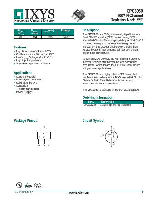
I NTEGRATED C IRCUITS D IVISIONCPC3960600V N-ChannelDepletion-Mode FETPart #DescriptionCPC3960ZTRSOT -223: T ape and Reel (1000/Reel)BV DSX /BV DGX R DS(on) (max)I DSS (min)Package 600V44Ω100mASOT -223ApplicationsFeaturesDescriptionOrdering InformationCircuit Symbol• Current Regulator • Normally-O n Switches • Solid State Relays • Converters• T elecommunications • Power Supply• High Breakdown Voltage: 600V • O n-Resistance: 44Ω max. at 25ºC • Low V GS(off) Voltage: -1.4 to -3.1V • High Input Impedance• Small Package Size: SOT -223The CPC3960 is a 600V , N-channel, depletion-mode, Field Effect T ransistor (FET) created using IXYSIntegrated Circuits Division’s proprietary vertical DMOS process. Yielding a robust device with high input impedance, this process enables world class, high voltage MOSFET performance with an economical silicon gate architecture.As with all MOS devices, the FET structure prevents thermal runaway and thermal-induced secondary breakdown, which makes the CPC3960 ideal for use in high-power applications.The CPC3960 is a highly reliable FET device that has been used extensively in IXYS Integrated Circuits Division’s Solid State Relays for industrial and telecommunications applications.The CPC3960 is available in the SOT -223 package.Package PinoutGDSAbsolute Maximum Ratings are stress ratings. Stresses in excess of these ratings can cause permanent damage to the device. Functional operation of the device at conditions beyond those indicated in the operational sections of this data sheet is not implied.Absolute Maximum Ratings @ 25ºCElectrical Characteristics @ 25ºC (Unless Otherwise Noted)Ratings Units Drain-to-Source Voltage 600V Gate-to-Source Voltage ±15V Pulsed Drain Current150mA Total Package Dissipation 1 1.8W Operational T emperature-55 to +125ºC Junction Temperature, Maximum +125ºC Storage Temperature-55 to +125ºC1 Mounted on 1"x1"2 oz. Copper FR4 board.Symbol Min Typ Max Units Drain-to-Source Breakdown Voltage BV DSX V GS = -5.5V , I D =100µA 600--V Gate-to-Source Off VoltageV GS(off)V DS = 15V , I D =1μA -1.4--3.1V Change in V GS(off) with Temperature dV GS(off) /dT V DS = 15V , I D =1μA -- 4.5mV/ºC Gate Body Leakage Current I GSS V GS =±15V , V DS =0V --100nA Drain-to-Source Leakage Current I D(off)V GS = -5.5V , V DS =600V --1µA Saturated Drain-to-Source CurrentI DSS V GS = 0V , V DS =15V 100--mA Static Drain-to-Source On-State Resistance R DS(on)V GS = 0V , I D =100mA, V DS =10V--44ΩChange in R DS(on) with T emperature dR DS(on) /dT-- 2.5%/ºC Forward T ransconductance G fs I D = 50mA, V DS = 10V100--m ΩInput CapacitanceC ISS V GS = -3.5VV DS = 25V f= 1MHz-100-pF Common Source Output Capacitance C OSS 6.8Reverse T ransfer Capacitance C RSS4.2Source-Drain Diode Voltage Drop V SD V GS = -5V , I SD =150mA-0.721V Thermal Resistance Junction to Ambient ΘJA --55-ºC/WJunction to CaseΘJC--23-PERFORMANCE DATA @ 25ºC (Unless Otherwise Noted)**The Performance data shown in the graphs above is typical of device performance. For guaranteed parameters not indicated in the written specifi cations, please contact our application department.V GS (V)-5-4-3-2-10I D (A )0.000.050.100.150.200.25Input Admittance(V=3V)Temperature (ºC)-50-250255075100125V G S (V )-3.5-3.0-2.5-2.0-1.5-1.0-0.50.0Threshold Voltage(I =1PA)I D (A)0.000.050.100.150.20-100100200300400Transconductance vs. Drain Current(V =3V)G m (m ):V DS (V)123456I D (m A )50100150200250Output CharacteristicsTemperature (ºC)-50-250255075100125O n -R e s i s t a n c e (:)1020304050On-Resistance vs. Temperature(V =0V, I=50mA)Temperature (ºC)-50-25255075100125L e a k a g e C u r r e n t (n A )020406080100120Leakage Current (V =-5V , V =600V)V DS (V)0510152025303540C a p a c i t a n c e (p F )50100150200Capacitance vs. Drain-Source Voltage(V =-5V)I D (A)0.00.10.20.30.40.50.6O n R e s i s t a n c e (:)5101520253035404550On-Resistance vs. Drain CurrentTemperature (ºC)020406080100120140P o w e r D i s s i p a t i o n (W )0.00.51.01.52.0Power Dissipationvs. Ambient TemperatureTemperature (ºC)-50-250255075100125B l o c k i n g V o l t a g e (V P )680700720740760780800Blocking Voltage vs. TemperatureVoltage (V)1101001000C u r r e n t (A )0.0010.010.11Forward Safe Operating Bias(V =0V , DC Load)Manufacturing InformationMoisture SensitivityAll plastic encapsulated semiconductor packages are susceptible to moisture ingression. IXYS IntegratedCircuits Division classified all of its plastic encapsulated devices for moisture sensitivity according tothe latest version of the joint industry standard, IPC/JEDEC J-STD-020, in force at the time of product evaluation. We test all of our products to the maximum conditions set forth in the standard, and guarantee proper operation of our devices when handled according to the limitations and information in that standard as well as to any limitations set forth in the information or standards referenced below.Failure to adhere to the warnings or limitations as established by the listed specifications could result in reduced product performance, reduction of operable life, and/or reduction of overall reliability.This product carries a Moisture Sensitivity Level (MSL) rating as shown below, and should be handled according to the requirements of the latest version of the joint industry standard IPC/JEDEC J-STD-033.DeviceCPC3960Z MSL 1ESD SensitivityThis product is ESD Sensitive, and should be handled according to the industry standard JESD-625. Reflow ProfileThis product has a maximum body temperature and time rating as shown below. All other guidelines of J-STD-020 must be observed.DeviceCPC3960Z260ºC for 30 secondsBoard WashIXYS Integrated Circuits Division recommends the use of no-clean flux formulations. However, board washing to remove flux residue is acceptable, and the use of a short drying bake may be necessary. Chlorine-based or Fluorine-based solvents or fluxes should not be used. Cleaning methods that employ ultrasonic energy should not be used.For additional information please visit our website at: IXYS Integrated Circuits Division makes no representations or warranties with respect to the accuracy or completeness of the contents of this publication and reserves the right to make changes to specifications and product descriptions at any time without notice. Neither circuit patent licenses nor indemnity are expressed or implied. Except as set forth in IXYS Integrated Circuits Division’s Standard T erms and Conditions of Sale, IXYS Integrated Circuits Division assumes no liability whatsoever, and disclaims any express or implied warranty, relating to its products including, but not limited to, the implied warranty of merchantability, fitness for a particular purpose, or infringement of any intellectual property right.The products described in this document are not designed, intended, authorized or warranted for use as components in systems intended for surgical implant into the body, or in other applications intended to support or sustain life, or where malfunction of IXYS Integrated Circuits Division’s product may result in direct physical harm, injury, or death to a person or severe property or environmental damage. IXYS Integrated Circuits Division reserves the right to discontinue or make changes to its products at any time without notice.Specification: DS-CPC3960-R02©Copyright 2015, IXYS Integrated Circuits Division Mechanical DimensionsCPC3960ZCPC3960ZTR Tape & ReelDimensions mm MIN / mm MAX (inches MIN / inches MAX)1.901.90PCB Land PatternDimensionsmm (inches)。
ETERNUS详细产品介绍

F6497C
Model 2200
60年代至今
1995年
1998年
2000年
2003年
2006年
2008年
未来更多 创新技术
F1710/F6491
ETERNUS GR840
ETERNUS 6000 ETERNUS 3000
ETERNUS 8000 ETERNUS 4000
磁盘阵列系统产品线
Enterprise storage systems
High Reliability High Performance Connectivity Storage Management
Tape Libraries
RAID Systems
Software
ETERNUS LT Tape Libraries
ETERNUS8000 ETERNUS4000 ETERNUS DX60/80
中端存储系统
INTERNAL USE ONLY
多控制器架构带来高性能
高性能控制器带来出色的 IOPS
CPU:采用高性能的四核处理器,较前代产品IOPS提升1.3倍,吞吐量提升1.2倍。 缓存:采用FB-DIMM,内存带库提高3 .3倍。 8GB主机接口: 率先在业界提供8Gbps FC接口,传输速率翻倍。
模块化结构
模块化架构合并了先进的控制器模块(CM)、通道适配器(CA)和设备适配器(DA),大大提高数据传输性能。 通过专用高速PCI-E总线相互连接控制器模块,带来很好的冗余性和高性能。
CA
Module configuration
CA
CA
CA
CM
CPU
■
■
CM
CPU
- 1、下载文档前请自行甄别文档内容的完整性,平台不提供额外的编辑、内容补充、找答案等附加服务。
- 2、"仅部分预览"的文档,不可在线预览部分如存在完整性等问题,可反馈申请退款(可完整预览的文档不适用该条件!)。
- 3、如文档侵犯您的权益,请联系客服反馈,我们会尽快为您处理(人工客服工作时间:9:00-18:30)。
•Multi-input modular instrument 4dgt LED •0.1% RDG basic accuracy•TRMS AC current and voltage measurements•AC/DC current measurements; selectable full scales (200µA to 5A)•AC/DC voltage measurements; selectable full scales (200mV to 500V)•°C or °F temperature measurements(Pt100-250-500-1000, Ni100, TC J-K-S-T -E)•Resistance measurements; selectable full scales (20Ωto 20k Ω)•Up to 4 independent alarm set-points (optional)•20mA/10VDC analog output (optional)•Serial port RS485 or RS232 (optional) •MODBUS, JBUS communication protocol •Front protection degree:IP67, NEMA4x•LED display, selectable colour (red, amber, green)Product Descriptionµp-based digital panel meter, 4-dgt LED indicator,for current, voltage, temper-ature and resistance mea-surements. Measuring ranges and functions easily programmable from the key-pad or from the PC bymeans of optional UdmSoft software. UDM 40includes storage min-max functions and double level protection password. Housing for panel mounting with front protec-tion degree: IP67, NEMA4x.Digital Panel MetersModular Indicator and Controller Type UDM40Type SelectionSlot A (measuring inputs)LSX:signal inputs:0.2-2-20mA DC/AC;0.2-2-20V DC/ACLSE/LSF:signal inputs: + AUX:0.2-2-20mA DC/AC;0.2-2-20V DC/ACHSX:signal inputs:0.2-2-5A DC/AC; 20-200-500V DC/ACTRX:signal inputs: TC tem-perature probes (J-K-S-T-E, Pt100-250-500-1000) and resistance (0.02-0.2-2-20k Ω)Slot B (communication)XX:NoneSX:Serial port RS485SY:Serial port RS232AV(*):Single analogue output, 0to 20mA DC and 0to 10V DC Slot C (communication and alarm)XX:NoneR1:Single relay output,(AC1-8AAC, 250VAC)R2:Dual relay output,(AC1-8AAC, 250VAC)R4:Dual relay output, (AC1-8AAC, 250VAC) +dualopen collector output (NPN, 100mA)R5:4relay outputs(AC1-5AAC, 250VAC)AV(*):Single analogue output,0to 20mA DC and 0to 10V DCSlot D (power supply)H:90 to 260V AC/DC L:18to 60V AC/DCOptions XX:NoneTX:TropicalizationInput Specifications•The alarm status can be coupled to the different colour of the display•Linearization of V and A inputs up to 16 pointsHow to orderUdmSoft-kitUdmSoft-kit: software plus “UCOM1” communication cable for programming UDM40 by means of PC .(*):The two analogue outputs cannot be used at the same time. It is possible to plug in only one module by instru-ment.Measurement accuracy , temp. drifts, max and min indicationsAll accuracies and min/max indications are referred to an ambient temp. range of 25°C ±5°C, rel. humidity ≤60% and scale ratio (electri-cal/displayed scale) equal to 1. The conversion into °F is obtained acting on the electrical/displayed scale ratio.*<45Hz >65Hz= ±(0.5%RDG+3DGT) 0% to 25% FS;±(0.5%RDG+2DGT) 25% to 110% FS.( )The min. indication for TRMS measurement (AC or DC) is 0; it is possible to modify the decimal point position.All accuracies and min/max indications refer to an ambient temperature range of 25°C ±5°C, relevant humidity ≤60% and scale ratio (elec-Input impedances and overloads(*) Maximum measuring current generated for resistance equal to 0UDM40Output specificationsUDM40Software functionsGeneral SpecificationsUDM40AC/DC voltage90 to 260V (standard)18 to 60V (on request)Energy consumption≤30VA/12W (90 to 260V)≤20VA/12W (18 to 60V)Supply SpecificationsAvailable modulesPossible module combinationsOnly for TRMS Measurements Instantaneous effective voltage (TRMS)å×=ni V nV 1211)(1å×=ni A n A 1211)(1Used calculation formulasInstantaneous effective current (TRMS)Insulation between inputs and outputsExcitation outputUDM40Wiring diagramsProcess signal wiring diagramsWirings for high-level signalsWiring diagrams of optional modulesBO R1: 1 relay outputBO R2: 2 relay outputs BO AV: analogue output (10V, 20mA DC)UDM40Wiring diagrams for temperature measurements Wiring diagrams (cont.)Wiring diagrams for power supplyBO R5: 4 relay outputsUDM40BO R4: dual relay output + dual open collector output: the load resistances (Rc) must be designed so that the close contact current is lower than 100mA; the VDC voltage must be lower than or equal to 30VDC.VDC: power supply outputVo+: positive output (open collector transistor).GND: ground collector (open collector transistor).BR SX: RS485 4-wire connection:additional devices provided with RS485 port (indicated as RS1,2,3...N) are connected in parallel. The termination of the serial port is carried out only on the last instrument of the network. The serial module is provided with a jumper for the termination of the RS485 network as shown in the figure above.Note:particular types of cables or plants may require an external termination. For the network connections use twisted cable type AWG26.RS1,2,3...NWiring diagrams of optional modules (cont.)VccUDM40 is programmable by PC by means of the UdmSoft software (available on request). The user can program all parameters of UDM40that will be subse-quently uploaded and set in the instrument by the RS485 network (BR SX).Should UDM40 be without the RS485 serial module, all programming parameters will be uploaded and set in the instrument by the RS232 auxiliary serial connec-tion (1) located on the side of the measuring input module using the special con-nection cable (2) available on request, as shown in the figures on the left. It is also possible to program the instrument using the dot connector (1) by means of the HyperTerminal Windows functions of a PC.Note:the RS232 auxiliary port IS NOT insulated from the measuring inputs. Ordering code of the cable (2): UCOM1Programming UDM40 by means of PCBO SY: RS232 directconnection to PC by means of COM port.RS232 has no termi-nalization.UDM40DimensionsFront panel description1.Key-padThe programming of the configuration parameters and the display may be easily controlled by means of the 4 function :to enter the programming phase and to confirm the Engineering UnitsSpecifications are subject to change without notice UDM40DS 04070611UDM40BP LPower supply:18 to 60V AC/DCBO R4Dual relay output +Dual open collectorBO R2Dual relay outputBO AVSingle analogueoutput 10V , 20mA DCBQ LSX, BQ LSE, BQ LSF , BQ HSX, BQ TRX Measuring inputs Input modulesSerial port modules BR SXRS485 Serial port BP HPower supply: 60 to 260V AC/DCModulesBO R1Single relay outputOutput modulesScale 1:1Power supply modulesOutput modulesBO R54relay outputsBR SYRS232 Serial port元器件交易网。