LF2050A-NH中文资料
CXA2050中文资料
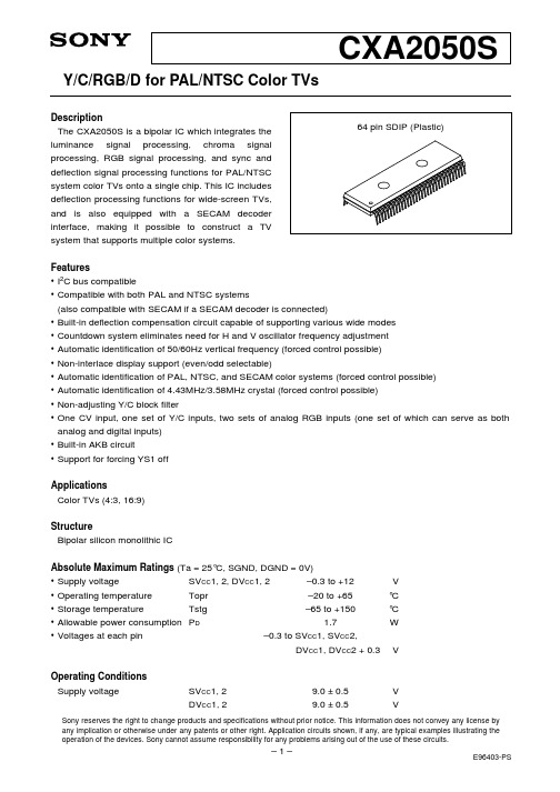
DescriptionThe CXA2050S is a bipolar IC which integrates the luminance signal processing, chroma signal processing, RGB signal processing, and sync and deflection signal processing functions for PAL/NTSC system color TVs onto a single chip. This IC includes deflection processing functions for wide-screen TVs,and is also equipped with a SECAM decoder interface, making it possible to construct a TV system that supports multiple color systems.Features•I 2C bus compatible•Compatible with both PAL and NTSC systems(also compatible with SECAM if a SECAM decoder is connected)•Built-in deflection compensation circuit capable of supporting various wide modes •Countdown system eliminates need for H and V oscillator frequency adjustment •Automatic identification of 50/60Hz vertical frequency (forced control possible)•Non-interlace display support (even/odd selectable)•Automatic identification of PAL, NTSC, and SECAM color systems (forced control possible)•Automatic identification of 4.43MHz/3.58MHz crystal (forced control possible)•Non-adjusting Y/C block filter•One CV input, one set of Y/C inputs, two sets of analog RGB inputs (one set of which can serve as both analog and digital inputs)•Built-in AKB circuit•Support for forcing YS1 off ApplicationsColor TVs (4:3, 16:9)StructureBipolar silicon monolithic ICAbsolute Maximum Ratings (Ta = 25°C, SGND, DGND = 0V)•Supply voltage SV CC 1, 2, DV CC 1, 2–0.3 to +12V •Operating temperature Topr –20 to +65°C •Storage temperature Tstg –65 to +150°C •Allowable power consumption P D 1.7W •Voltages at each pin –0.3 to SV CC 1, SV CC 2,DV CC 1, DV CC 2 + 0.3V Operating Conditions Supply voltageSV CC 1, 29.0 ±0.5V DV CC 1, 29.0 ±0.5VCXA2050SY/C/RGB/D for PAL/NTSC Color TVsSony reserves the right to change products and specifications without prior notice. This information does not convey any license by any implication or otherwise under any patents or other right. Application circuits shown, if any, are typical examples illustrating the operation of the devices. Sony cannot assume responsibility for any problems arising out of the use of these circuits.64 pin SDIP (Plastic)CXA2050SB l o c k D i a g r a mI R E FA P C F I LX 358X 443F S C O U TS E C A M R E F– (R -Y ) O U T – (B -Y ) O U TY O U TY R E T– (R -Y ) I N– (B -Y ) I NY S 1/V MR 1I NG 1I NB 1I NY S 2Y MR 2I NG 2I NB 2I NA B L F I LK I N O U TO U TO U T -W O U T D – O U T V P R O T D + O U T V P R O T A W O S C A G C S H T I MC P O U TD O U TG N DV C C 2V C C 1A B L I N /V C O M PR S HG S HB S HL 2F I LA F C P I N /H O F FC E R AF C F I LH S I NS I NV S F I LB L H O L DD C T R A NV MS C LS D AS Y N C O U TE X T S Y N C I NC V I N Y I N C I N S V C C 1S V C C 2S G ND 1S G N D 2V I DE O O U TS V C C 1A P C F I LX 443X 358T E S TF S C O U TS E C A M R E FS G N D 1– (R -Y ) O U TY O U TS C P O U TY R E TS G N D 2Y S 1/V MR 1I NG 1I NB 1I NY S 2Y MR 2I NG 2I NB 2I NS V C C 2R S HR O U TG S HG O U TB S HB O U T– (B -Y ) O U T– (R -Y ) I N– (B -Y ) I NC I NE X T S Y N C I NY I ND C T R A NC V I NB L H O L DV I D E O O U TS D AS C LV MS Y N C O U TH S I NV S I NV S F I LD V C C 2I R E FD G N DC E R AA F C F I LL 2F I L A F C P I N /H O F FH D O U TD V C C 1S A W O S CV A G C S HE -W O U TV D + O U T /V P R O TV T I MA B L F I LA B L I N /V C O M PI K I NV D – O U T /V P R O TCXA2050SE l e c t r i c a l C h a r a c t e r i s t i c s S e t t i n g c o n d i t i o n s •T a = 25°C , S V C C 1, 2 = D V C C 1, 2 = 9V , S G N D 1, 2 = D G N D = 0V •M e a s u r e s t h e f o l l o w i n g a f t e r s e t t i n g t h e I 2C b u s r e g i s t e r a s s h o w n i n “I 2C B u s R e g i s t e r I n i t i a l S e t t i n g s ”.元器件交易网元器件交易网CXA2050S元器件交易网CXA2050S元器件交易网CXA2050S元器件交易网CXA2050SE l e c t r i c a l C h a r a c t e r i s t i c s M e a s u r e m e n t C i r c u i tS i g n a l s o u r c e sr e a l l G N D u n l e s s o t h e r w i s e s p e c i f i e d i n t h e M e a s u r e m e n t c o n d i t i o n s c o l u m n o f E l e c t r i c a l C h a r a c t e r i s t i c s .P R O Tf r o m H D O U H P G E N .A p p l i c a t i o n C i r c u i tS E C A M r e f e i n p u t /o u t p u t f .001µC o l o r d i f f e r e n f o r 1H d e l a y l i S a n d c a s t l C o l o r d i f f e r e f r o m 1H d e l a A n a l o g A n a l o g /d i g i t a l R G Y S 1/V M t e r n ∗1 M e t a l f i l m r e s i s t o r r e c o m m e n d e d ∗2 M P S c a p a c i t o r r e c o m m e n d e di g h v o l t a g e f l u c t u a t i o ns i g n a l i n p u tu t p u t sp r o t e c t s i g n a l i n p u tu tH D o u t p u tH P o u t p u tn i n p u tu to u t p u tp u tA p p l i c a t i o n c i r c u i t s s h o w n a r e t y p i c a l e x a m p l e s i l l u s t r a t i n g t h e o p e r a t i o n o f t h e d e v i c e s . S o n y c a n n o t a s s u m e r e s p o n s i b i l i t y f o r a n y p r o b l e m s a r i s i n g o u t o f t h e u s e o f t h e s e c i r c u i t s o r f o r a n y i n f r i n g e m e n t o f t h i r d p a r t y p a t e n t a n d o t h e r r i g h t d u e t o s a m e .Electrical Characteristics Measurement Conditions “I2C Bus Register Initial Settings”Register name No. ofbitsInitialsettingDescriptionPICTURE TRAPOFF VMHUE DCTRAND-PIC COLORTOTABL BRIGHTD-COL LIMIT SHARPNESS PRE-OVER COLOR SW SUB-CONT TRAP F0 SUB-COLOR SUB-HUE SUB-BRIGHT GAMMAG-DRIVE AGINGB-DRIVE INTERLACE G-CUTOFF B-CUTOFF RONGONBONPICON VOFFFHHICD-MODE AKBOFFV-SIZE 6116116116114224444626162441111111163Fh1h1h1Fh0h0h1Fh0h1Fh0h7h3h0h7h7h7h7h1Fh0h2Ah0h2Ah0h0h0h1h1h1h1h0h0h0h0h1FhMaximum valueTRAP offMaximum valueCenter valueDCTRAN offDPIC offCenter valueTOT offPicture/bright ABL modeCenter valueDCOL offLimiter offCenter valueMaximum valueAutomatic switchingCenter valueCenter valueCenter valueCenter valueCenter valueMinimum valueCenter valueAGING offCenter valueInterlaceMinimum valueMinimum valueR output onG output onB output onPicture mute offVD output onFH normalAutomatic switchingAKB onCenter valueV FREQV-POSITIONAFC-MODES-CORRV-LINH-SIZEREF-POSIPIN-COMPVBLKWH-POSITOPNPIN-PHASEAFC-BOWAFC-ANGLEEHT HEHT VXTALEXT SYNCCV/YCV-ASPECTZOOM SWHBLKSWV-SCROLLJMPSWHSIZESWUP-VLINLO-VLINLEFT-BLKRIGHT-BLKUP-CPINLO-CPINCDMODE2SHPF0YS1OFFDL26244626244442221161161144444411130h1Fh1h0h7h1Fh3h1Fh0h7h7h7h7h0h0h0h0h0h0h0h0h1Fh0h0h0h0h7h7h7h7h0h3hAutomatic switchingCenter valueLow gainMinimum valueCenter valueCenter valueMaximum valueCenter valueMinimum valueCenter valueCenter valueCenter valueCenter valueEHT H offEHT V offAutomatic switchingInternal syncCV inputMinimum valueZOOM SW offHBLKSW offCenter valueJMPSW offHSIZESW offMinimum valueMinimum valueCenter valueCenter valueCenter valueCenter valueStandard mode3MHzYS1 normalCenter valueRegisternameNo. ofbitsInitialsettingDescriptionTRAP F0SUB-HUEB-CUTOFFV-LINPIN-PHASE AFC-ANGLELO-VLIN RIGHT-BLK LO-CPINPICTURE HUE COLOR BRIGHTSUB-BRIGHT G-DRIVE B-DRIVEV-SIZE V-POSITIONH-SIZE PIN-COMPV-ASPECT V-SCROLLSHARPNESSSUB-CONT SUB-COLORG-CUTOFF S-CORRH-POSITION AFC-BOWUP-VLIN LEFT-BLK Definition of I 2C Bus Registers Slave Addresses88h:Slave Receiver 89h: Slave TransmitterRegister Table"∗": Undefined Control RegisterBit0Bit1Bit2Bit3Bit4Bit5Bit6Bit7Sub Address ×××0 0 0 0 0 00 h ×××0 0 0 0 1 01 h ×××0 0 0 1 0 02 h ×××0 0 0 1 1 03 h ×××0 0 1 0 0 04 h ×××0 0 1 0 1 05 h ×××0 0 1 1 0 06 h ×××0 0 1 1 1 07 h ×××0 1 0 0 0 08 h ×××0 1 0 0 1 09 h ×××0 1 0 1 0 0A h ×××0 1 0 1 1 0B h ×××0 1 1 0 0 0C h ×××0 1 1 0 1 0D h ×××0 1 1 1 0 0E h ×××0 1 1 1 1 0F h ×××1 0 0 0 0 10 h ×××1 0 0 0 1 11 h ×××1 0 0 1 0 12 h ×××1 0 0 1 1 13 h ×××1 0 1 0 0 14 h ×××1 0 1 0 1 15 h ×××1 0 1 1 0 16 h ×××1 0 1 1 1 17 h ×××1 1 0 0 0 18 h ×××1 1 0 0 1 19 hTRAPOFF DC-TRAN TOT D-COLVM D-PIC ABL LIMITPRE-OVERCOLOR SWGAMMA AGING0AKBOFFCD-MODE FHHIVOFFPICONBONGONRONV-FREQ AFC-MODEREF-POSI VBLKWEXT SYNC ZOOM SW JMP SW CV/YC HBLKSW HSIZESW Status RegisterBit0FVBit1FSCBit2Bit3Bit4XRAYBit5VNGBit6IKRBit7H LOCKINTERLACEEHT HEHT V XTALUP-CPINCDMODE2SHPF0∗YS1 OFFDL∗COLOR SYSDescription of RegistersRegister name (No. of bits)1. Video switch registerCV/YC(1):CV input/YC input selector0 = CV input selected1 = YC input selectedEXT SYNC(1):EXT SYNC selector switch0 = Internal sync (CV or Y) selected1 = EXT SYNC selected2. Y signal block registerSUB-CONT(4):Contrast gain control (Y gain control)0h = –3.5dB7h = 0dBFh = +2.5dBTRAP-F0(4):Chroma trap f0 fine adjustment0h = High7h = CenterFh = LowSHARPNESS(4):Sharpness gain control0h = –6dB7h = +2.5dBFh = +6.5dBSHPF0(1):Sharpness f0 selector0 = 3MHz1 = 3.5MHzPRE-OVER(2):Sharpness preshoot/overshoot ratio control0h = 1:1(PRE: OVER)3h = 2:1VM(1):Y differential signal output level selector for VM (for 100% 3MHz input)0 = 1.1Vp-p1 = 2.65Vp-pTRAP OFF(1):Y block chroma trap ON/OFF0 = Trap ON1 = Trap OFFDL(3):Y signal delay time control (80ns/step)0h = Max.7h = Min.DC-TRAN(1):Y DC transmission ratio selector switch0 = 100%1 = 81%D-PIC(1):Y black expansion ON/OFF switch0 = OFF1 = ON Point of inflection: 30 IRE3. C signal block registerTOT(1):Chroma TOT filter band selector switch0 = TOT — TRAP OFF1 = TOT — TRAP ON (TRAP fo 2MHz)COLOR(6):Color gain control (Chroma gain control)0h = Color OFF (–40dB or less)1Fh = 0dB B output: 1.02Vp-p (I/O gain: +11dB, 0.285Vp-p input)3Fh = +6dBSUB-COLOR(4):Color gain control (ACC reference level control)0h = –5dB7h = 0dBFh = +3dBHUE(6):Hue control (Phase control for chroma demodulation axis when SUB-HUE is 7h) Control not possible for a PAL system.0h = +35°Flesh color appears red.1Fh = 0°3Fh = –35°Flesh color appears green.SUB-HUE(4):Hue control (Phase control for chroma demodulation axis when HUE is 1Fh)B-Y axis adjustable to 0°.Control not possible for a PAL system.0h = +10°7h = 0°Fh = –10°XTAL(2):XTAL selection setting switch0h = Automatic identification1h = Force to XTAL1 (3.58MHz)2, 3h = Force to XTAL2 (4.43MHz)COLOR SW(2):Color system setting0h = Automatic identification1h = Force to PAL2h = Force to NTSC3h = Force to SECAM4. RGB signal block registerPICTURE(6):Picture gain control (RGB gain control)0h = –14dB3Fh = 0dB RGB output: 2.5Vp-p (I/O gain: +8dB, 1Vp-p input)BRIGHT(6):Bright control (RGB DC bias control)0h = –420mV1Fh = 0mV(–300mV for REF-P level)3Fh = +420mVSUB-BRIGHT(6):Bright control (RGB DC bias control)0h = –420mV1Fh = 0mV(–300mV for REF-P level)3Fh = +420mVG-DRIVE(6):Gch drive gain adjustment (Gch gain control)0h = G/R –4.5dB2Ah = G/R 0dB (G/R 0dB)3Fh = G/R +1.5dBB-DRIVE(6):Bch drive gain adjustment (Bch gain control)0h = B/R –4.5dB2Ah = B/R 0dB (B/R 0dB)3Fh = B/R +1.5dBG-CUTOFF(4):Gch cut-off adjustment (Gch reference pulse value control of IKIN pin input)0h = +34%7h = +81% (G/R)Fh = +135%B-CUTOFF(4):Bch cut-off adjustment (Bch reference pulse value control of IKIN pin input)0h = +34%7h = +81% (B/R)Fh = +135%D-COL(1):Dynamic color ON/OFF switch0 = Dynamic color OFF1 = Dynamic color ON (R, Bch level control)GAMMA(2):Gamma control (RGB gamma correction amount control)0h = Gamma OFF3h = Gamma peak 17 IRE (at input 40 IRE), +400mV (at 2.5Vp-p OUT)REF-POSITION (2):Reference pulse timing setting0h = From rising edge of V TIM: Rch 22H, Gch 23H, Bch 24H1h = From rising edge of V TIM: Rch 20H, Gch 21H, Bch 22H2h = From rising edge of V TIM: Rch 18H, Gch 19H, Bch 20H3h = From rising edge of V TIM: Rch 16H, Gch 17H, Bch 18HPIC-ON(1):ON/OFF switch for RGB output with a reference pulse(Set to OFF mode at power-on.)0 = RGB output OFF (All blanked status)1 = RGB output ONR ON(1):ON/OFF switch for Rch video output without a reference pulse(Operates when PIC ON = 1, set to OFF mode at power-on.)0 = Rch video output OFF (Blanked status, reference pulse only output)1 = Rch video output ONG ON(1):ON/OFF switch for Gch video output without a reference pulse(Operates when PIC ON = 1, set to OFF mode at power-on.)0 = Gch video output OFF (Blanked status, reference pulse only output)1 = Gch video output ONB ON(1):ON/OFF switch for Bch video output without a reference pulse(Operates when PIC ON = 1, set to OFF mode at power-on.)0 = Bch video output OFF (Blanked status, reference pulse only output)1 = Bch video output ONAKB OFF(1):AKB ON/OFF switch (Set to ON mode at power-on.)0 = AKB ON1 = AKB OFF (IK CLAMP, IK S/H and reference pulse fixed to OFF)R, G and B cut-off adjustment at AKB OFF performed by voltage applied to RSH,GSH and BSH pins, respectively.YS1 OFF(1):YS1 forced OFF mode/YS1 normal mode0 = YS1 normal mode1 = YS1 forced OFF modeABL(1):ABL mode selector0 = Picture/bright ABL mode1 = Picture ABL modeLIMIT(1):Peak limiter (RGBOUT pin is limited at DC5.2V)0 = OFF1 = ON5. Deflection block registerAFC-MODE(2):AFC loop gain control (PLL between H SYNC and H VCO)0h = H free run mode1h = Small gain2h = Medium gain3h = Large gainFH-HI(1):H oscillator frequency fixation ON/OFF switch(Set to ON mode at power-on.)0 = H oscillator frequency fixation OFF AFC normal mode1 = H oscillator frequency fixation ON Oscillator frequency fixed to maximum value(approx. 16.2kHz)V FREQ(1):V frequency mode setting0, 1h = Automatic identification2h = Forced mode (50Hz)3h = Forced mode (60Hz)V OFF(1):V sawtooth wave oscillation stop ON/OFF switch(Set to OFF mode at power-on.)0 = Oscillation stop OFF (V DRIVE– and V DRIVE+: normal output)1 = Oscillation stop ON (V DRIVE– and V DRIVE+: DC output and DC value varyaccording to V POSITION.)CD-MODE(1):V countdown system mode selector(Set to automatic selection mode during power-on.)0 = Non-standard signal mode, standard signal mode and no signal modeautomatically selected1 = Fixed to non-standard signal mode(V oscillator frequency is 55Hz during no signal mode "free run".)CDMODE2(1):Vertical sync pull-in speed selector0 = Standard1 = High speedVBLKW(2):VBLK width control (Blanked pulses after reference pulse. Operates whenJMPSW = 1; blanked pulses after reference pulse fixed to 1H when JMPSW = 0.)0h = 12H from Bch reference pulse1h = 11H from Bch reference pulse2h = 10H from Bch reference pulse3h = 9H from Bch reference pulseH-POSITION(4):Horizontal position adjustment (HAFC phase control)0h = 1µs delay Picture position shifts to right. (Picture delayed with respect to HD.)7h = 0µsFh = 1µs advance Picture position shifts to left. (Picture advanced with respect to HD.)V-POSITION(6):Vertical position adjustment (V SAW output DC bias control)0h = –0.09V Picture position drops, V DRIVE+ output DC Down.1Fh = 0V Center potential: DC 3V3Fh = +0.09V Picture position rises, V DRIVE+ output DC Up.CXA2050S V-SIZE(6):Vertical amplitude adjustment (V SAW output gain control)0h = –14%Vertical picture size decreases.1Fh = 0%Amplitude: 1.23Vp-p, center potential: DC 3V when V-ASPECT is 2Fh.3Fh = +14%Vertical picture size increases.V-LIN(4):Vertical linearity adjustment (Gain control for V SAW secondary component)0h = 115%(Bottom/top of picture) Top of picture compressed; bottom of pictureexpanded.7h = 100%(Bottom/top of picture)Fh = 85%(Bottom/top of picture) Top of picture expanded; bottom of picturecompressed.S-CORR(4):Vertical S correction amount adjustment (V SAW secondary component gain control) 0h = Secondary component amplitude by adding sawtooth = 0Fh = Secondary component amplitude by adding sawtooth = MaximumAFC-BOW(4):Vertical line bow compensation amount adjustment (Phase control according toHAFC parabola wave)0h = Top and bottom of picture delayed 500ns with respect to picture center.7h = 0 nsFh = Top and bottom of picture advanced 500ns with respect to picture center.AFC-ANGLE(4):Vertical line slope compensation amount adjustment (Phase control according toHAFC V SAW)0h = Top of picture delayed 400ns, bottom of picture advanced 400ns with respect topicture center.7h = 0 nsFh = Top of picture advanced 400ns, bottom of picture delayed 400ns with respect topicture center.PIN-COMP(6):Horizontal pin distortion compensation amount adjustment (V parabola wave gaincontrol)0h = 0.10Vp-p Horizontal size for top/bottom of picture increases. (Compensationamount minimum)1Fh = 0.58Vp-p Amplitude, center potential: DC 4V when V-ASPECT is 0h3Fh = 1.06Vp-p Horizontal size for top/bottom of picture decreases. (Compensationamount maximum)H-SIZE(6):Horizontal amplitude adjustment (V parabola wave DC bias control)0h = –0.5V Horizontal picture size decreases, EW-DRIVE output DC Down.1Fh = 0V Amplitude: 0.58Vp-p, center potential: DC 4 V when V-ASPECT is 2Fh3Fh = +0.5V Horizontal picture size increases, EW-DRIVE output DC Up.EHT-H(2):Horizontal high-voltage fluctuation compensation amount setting (DC adjustment for parabolic output)0h = 0V (Compensation amount when 1V is applied to ABL IN versus 8V appliedto ABL IN)3h = –0.1V (Compensation amount when 1V is applied to ABL IN versus 8V appliedto ABL IN)EHT-V(2):Vertical high-voltage fluctuation compensation amount setting (V SAW output gain control) 0h = 0% (Compensation amount when 1V is applied to ABL IN versus 8V applied toABL IN)3h = –7% (Compensation amount when 1V is applied to ABL IN versus 8V applied toABL IN)INTERLACE(1):Interlace mode and non-interlace display selector switch0,1h = Interlace mode2h = Interlace mode; 1/2H shift applied to EVEN lines3h = Interlace mode; 1/2H shift applied to ODD linesCXA2050S PIN-PHASE(4):Horizontal trapezoidal distortion compensation amount adjustment (V parabola wave center timing control)0h = 0.8ms advance Horizontal size for top of picture increases; horizontal size forbottom of picture decreases.7h = 0ms8.9ms from 4VDC VTIMFh = 0.8ms delay Horizontal size for top of picture decreases; horizontal sizefor bottom of picture increases.UP-CPIN(4):Horizontal pin distortion compensation amount adjustment for top of picture(V parabola wave gain control: Func.)0h = +0.6V Horizontal size for top of picture increases.(compensation amount minimum)7h = 0V(0.7Vp-p 4:3 mode)Fh = –0.6V Horizontal size for top of picture decreases.(compensation amount maximum)LO-CPIN(4):Horizontal pin distortion compensation amount adjustment for bottom of picture(V parabola wave gain control: Func.)0h = +0.5V Horizontal size for bottom of picture increases.(compensation amount minimum)7h = 0V(0.7Vp-p 4:3 mode)Fh = –0.5V Horizontal size for bottom of picture decreases.(compensation amount maximum)V-ASPECT(6):Aspect ratio control (Gain control for sawtooth wave)0h = 75%16:9 CRT full2Fh = 100%4:3 CRT full, amplitude: 1.32Vp-p3Fh = 112%ZOOM SW(1):Zoom mode ON/OFF switch for 16:9 CRT (25% of video cut)0 = Zoom OFF Sawtooth wave amplitude: 1.32Vp-p1 = Zoom ON Sawtooth wave amplitude: 70%HBLKSW(1):HBLK width control ON/OFF switch during 4:3 software full display mode on a 16:9 CRT0 = Control OFF HBLK pulse generated from HPIN.1 = Control ON HBLK pulse generated as pulse generated from HPIN or aspulse generated from HVCO and width adjusted.Width adjustment is performed by the LEFT-BLK andRIGHT-BLK registers.V-SCROLL(6):Vertical picture scroll control during zoom mode on a 16:9 CRT(DC component added to sawtooth wave AGC output to control ZOOMSW cuttiming.)0h = –0.2V Scrolled toward top of screen by 32H and top of picture zoomed.1Fh = 0V3Fh = +0.2V Scrolled toward bottom of screen by 32H and bottom of picture zoomed. JUMPSW(1):Reference pulse jump mode ON/OFF switch (In addition to V-ASPECT control, sawtooth wave gain control performed for 100% of VBLK interval and 67% of picture interval)0 = Jump mode OFF1 = Jump mode ONOn a 4:3 CRT, jump mode expands the sawtooth wave amplitude to 112% with V-ASPECT; on a 16:9 CRT, jump mode compresses the sawtooth wave amplitude to75% with V-ASPECT. The V blanking width is expanded at both the top and bottomof the picture. Blanking for the bottom of the picture starts 251H after VTIM, andblanking for the top of the picture can be varied as the blanking width after thereference pulse from the VBLKW register.CXA2050S HSIZESW(1):Lowers the E-W OUT DC level (during H-SIZE compression)0 = Normal1 = –1.35VUP-VLIN(4):Vertical linearity adjustment for top of picture (Secondary component gain control for sawtooth wave added to sawtooth wave AGC output)0h = 100%(Bottom/top of picture)Fh = 115%(Bottom/top of picture) Top of picture compressed.LO-VLIN(4):Vertical linearity adjustment for bottom of picture (Tertiary component gain controlfor sawtooth wave added to sawtooth wave AGC output)0h = 100%(Bottom/top of picture)Fh = 75%(Bottom/top of picture) Bottom of picture compressed.LEFT-BLK(4):HBLK width control for the left side of picture when HBLKSW = 1 (Phase control for timing pulse generated from HVCO)0h = +1.7µs HBLK width maximum7h = 0µs Center HBLK: 15µsFh = –1.7µs HBLK width minimumRIGHT-BLK(4):HBLK width control for the right side of picture when HBLKSW = 1 (Phase control for timing pulse generated from HVCO)0h = +1.7µs HBLK width maximum7h = 0µs Center HBLK: 15µsFh = –1.7µs HBLK width minimum6. OtherAGING(1):White output aging mode ON/OFF switch(Takes priority over RGB ON and PIC ON control. Set to OFF mode at power-on.)0 = Aging mode OFF1 = Aging mode ON (When there is no input signal, a 60 IRE flat signal is outputfrom the Y block)7. Status registerHLOCK(1):Lock status between H SYNC and H VCO0 = HVCO free run status1 = Locked to H SYNCIKR(1):AKB operation status0 = REF-P at Ik small and AKB loop unstable.1 = REF-P at Ik sufficient and AKB loop stable.VNG(1):Signal input status to V PROT pin0 = No V PROT input1 = V PROT input (In this case, the RGB output is blanked.)XRAY(1):Signal input status to XRAY control pin (HOFF pin)0 = No XRAY control input1 = XRAY control input (In this case, the RGB output is blanked.)COLOR SYS(2):Color system status0h = PAL1h = NTSC2h = SECAM3h = NO STANDARDFSC(1):X’tal status (Fsc information)0 = 4.43MHz1 = 3.58MHzFV(1):Vertical deflection frequency status0 = 50Hz1 = 60HzDescription of Operation1. Power-on sequenceThe CXA2050S does not have an internal power-on sequence. Therefore, power-on sequence is all controlled by the set microcomputer (I2C bus controller).1) Power-onThe IC is reset and the RGB outputs are all blanked. Hdrive starts to oscillate, but oscillation is at the maximum frequency (16kHz or more) and is not synchronized to the input signal. Output of vertical signal VTIM starts, but Vdrive is DC output. Bus registers which are set by power-on reset are as follows.AGING= 0: All white output aging mode OFFRON= 0: Rch video blanking ONGON= 0: Gch video blanking ONBON= 0: Bch video blanking ONPICON= 0: RGB all blanking ONVOFF= 1: VDRIVE output stopped modeVFREQ= 0: Automatic identification mode (identification starts at 50Hz)FHHI= 1: H oscillator maximum frequency modeHSIZESW= 0: NormalCD-MODE= 0: Automatic selector mode of the countdown modeAKBOFF= 0: AKB mode2) Bus register data transferThe register setting sequence differs according to the set sequence. Register settings for the following sequence are shown as an example.Set sequence CXA2050S register settingsPower-on Reset status in 1) above.↓↓Degauss Reset status in 1) above.The CRT is degaussed in the completely darkened condition.↓↓VDRIVE oscillation The IC is set to the power-on initial settings. (See the following page.)A sawtooth wave is output to VDRIVE and the IC waits for the verticaldeflection to stabilize. The HDRIVE oscillator frequency goes to the standardfrequency.↓↓AKB operation start PICON is set to 1 and a reference pulse is output from Rout, Gout and Bout.Then, the IC waits for the cathode to warm up and the beam current to startflowing.↓↓AKB loop stable Status register IKR is monitored.IKR = 0: No cathode currentIKR = 1: Cathode currentNote that the time until IKR returns to 1 differs according to the initial statusof the cathode.↓↓Video output RON, GON and BON are set to 1 and the video signal is output from Rout,Gout and Bout.11010110001000100110101111Bit0Bit1Bit2Bit3Bit4Bit5Bit6Bit7Sub Address ×××0 0 0 0 0 00 h ×××0 0 0 0 1 01 h ×××0 0 0 1 0 02 h ×××0 0 0 1 1 03 h ×××0 0 1 0 0 04 h ×××0 0 1 0 1 05 h ×××0 0 1 1 0 06 h ×××0 0 1 1 1 07 h ×××0 1 0 0 0 08 h ×××0 1 0 0 1 09 h ×××0 1 0 1 0 0A h ×××0 1 0 1 1 0B h ×××0 1 1 0 0 0C h ×××0 1 1 0 1 0D h ×××0 1 1 1 0 0E h ×××0 1 1 1 1 0F h ×××1 0 0 0 0 10 h ×××1 0 0 0 1 11 h ×××1 0 0 1 0 12 h ×××1 0 0 1 1 13 h ×××1 0 1 0 0 14 h ×××1 0 1 0 1 15 h ×××1 0 1 1 0 16 h ×××1 0 1 1 1 17 h ×××1 1 0 0 0 18 h ×××1 1 0 0 1 19 h111111111110111111100111111111111111101111111101111∗1111111111101111111101111∗11110001110011011000010100111101111110111111100111100001011000100110011010111110000000000000000000000000I 2C bus power-on initial settingsThe initial settings listed here for power-on when VDRIVE starts to oscillate are reference values; the actual settings may be determined as needed according to the conditions under which the set is to be used.Register Table“∗” Undefined Control Register。
2050型智能空气 TSP综合采样器
-200.0°C~1300.0°C
-200~-100℃:1.0℃
-100~900℃:0.7℃
900~1300℃:0.8℃
B
400°C~1800°C
1°C
400~600℃:2.0℃
600~800℃:1.5℃
800~1800℃:1.1℃
热电阻
RTD
PT100
-200.0°C~850.0°C
0.1°C
-200~0℃:0.3℃
11、采用面板校准技术,无需打开机壳便可进行校准
测量基本技术指标[适用于校准后一年内、23℃±5℃、0~70%RH、精度=±(%读数+LSD)
测量功能
量程
测量范围
分辨力
精度
备注
直流电压DCV
50mV
-5.000mV~55.000mV
1μV
0.02%+10
输入阻抗:约100MΩ
500mV
-10.00mV~550.00mV
100KHz
1KHz
回路电源
LOOP
24V
±10%
最大输出电流约25mA
有短路保护
压力PRESS
2.49KPa
~
70MPa
0.025%量程
参考精度
0.05%量程
整体精度
可配用APM系列32个品种的压力模块,提供了用于差压、表压、真空压力、绝对压力、双压和高压的模块;有关详细技术指标,请参阅相关的压力模块技术资料
3、测量功能:直流电压、直流电流、欧姆、频率、热电偶、热电阻、开关量测量测量值的显示保持及平均值处理、内部提供24V回路电源
4、输出功能:直流电压、直流电流、欧姆、模拟变送器、热电偶、热电阻、频率、脉冲、开关量、压力、内部提供24V回路电源
EEEHP1A100R中文资料(panasonic)中文数据手册「EasyDatasheet - 矽搜」
61
0.50 EEEHB0G101R
82
0.50 EEEHB0G151P
82
0.50 EEEHB0G221P
26
0.30 EEEHB0J220R
29
0.30 EEEHB0J330R
46
0.30 EEEHB0J470R
71
0.30 EEEHB0J101P
150
0.35 EEEHB0J221P
230
0.35 EEEHB0J331P
00 Nov. 2012
芯片中文手册,看全文,戳
铝电解电容器/ HB
■ 标准产品
W.V.
Cap. (±20 %)
机箱尺寸
Dia. 长度
尺寸 代码
(V) (µF) 47
(毫米) (毫米)
4
5.8
B
100
5
5.8
C
4
150
6.3
5.8
D
220
6.3
5.8
D
22
4
5.8
B
33
4
5.8
B
500
(2)
500
Design and specifications are each subject to change without notice. Ask factory for the current technical specifications before purchase and/or use. Should a safety concern arise regarding this product, please be sure to contact us immediately.DΒιβλιοθήκη 25478
2050说明书4.0
目录第一章系统概述 (1)1.1适用范围 (1)1.2主要特点 (1)第二章技术参数 (2)2.1通用参数 (2)2.2电气性能 (3)2.2.1绝缘电阻 (3)2.2.2介质强度 (3)2.2.3冲击电压 (3)2.2.4抗电磁干扰性能 (3)2.2保护、测控、通讯参数 (4)第三章装置功能及原理 (5)3.1保护配置和定值整定原理 (5)3.1.1低电压保护 (5)3.1.2过电压保护 (5)3.1.3零序过电压保护 (6)3.1.4PT断线检查 (6)3.1.5开关量保护 (7)3.1.6定值清单 (7)3.1.7保护逻辑框图 (8)3.2测控原理 (9)3.2.1遥测采集和计算 (9)3.2.2遥信采集 (9)3.2.3遥脉采集 (9)3.2.4遥控输出 (9)3.2.5通讯 (10)3.2.6对时 (10)3.2.7统计 (10)3.3自检功能 (10)3.4选配功能 (10)第四章装置使用说明 (11)4.1整体配置 (11)4.2面板说明 (11)4.2.1液晶显示屏 (12)4.2.2信号指示灯 (12)4.2.3调试口 (12)4.2.4按键 (12)4.3显示说明 (14)4.4模件说明 (17)4.5机械结构 (19)4.6背板布局及端子号 (19)4.7装置硬件接线图 (19)第五章安装调试与投运 (20)5.1安装前检查 (20)5.2装置通电检查 (20)5.3调试 (20)5.4投运说明及注意事项 (21)第六章订货须知 (22)第一章系统概述1.1 适用范围HN-2050 PT保护测控装置是在总结本公司多年继电保护研发和工程经验的基础上,参考国内外相关成果,应用先进的软、硬件技术和专利抗干扰技术研制而成,符合继电保护四统一的要求,适用于35KV及以下电压等级PT柜中电压互感器监测和电压保护。
1.2 主要特点保护原理成熟可靠,并经历长时间的现场运行考验带有测控功能,计算精度高,能实现四遥功能,是四合一保护产品可采用CAN网、以太网等通讯方式,以单网、双网方式与监控系统通讯,通讯速度快,可靠性高保护功能与通讯功能相互独立,任何通信故障不影响保护单元的正常运行具有本地或远方操作功能装置可存入多套定值,定值可以本地或远方整定采用硬件实时时钟,装置掉电后仍连续计时,并采用GPS、通讯对时采用大屏幕液晶中文显示,人机界面友好,信息详细直观,操作、调试方便面板上有专用调试口,便于调试、整定和维护装置具有故障录波功能及32次带时间信息的保护动作顺序事件记录,且具有掉电保持功能装置具有自检功能,菜单中带有开出试验选项,便于调试、检验采用与本系列其它产品统一的软硬件平台,便于调试和维护通讯采用统一编码设计,伸缩性和扩展性好装置为分板插件整面板式结构,封闭、加强型单元机箱,抗强振动、强干扰设计,适应于恶劣环境采用模块化设计,软硬件兼容性好装置具有独立的交流电流电压输入、输出回路,及独立的具有防跳功能的操作回路(适用于断路器回路或FC回路)可分散安装于开关柜上,也可集中组屏安装第二章技术参数2.1 通用参数2.2 电气性能2.2.1 绝缘电阻在标准试验大气条件下,装置各带电的导电回路对地之间,及电气上无联系的各带电的导电回路之间,用开路电压500V摇表测其绝缘电阻应不小于100MΩ。
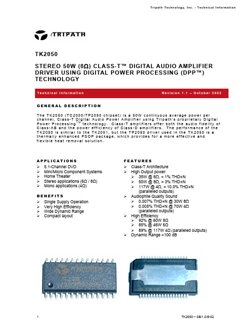
TK2050中文资料
SYMBOL V5 Vlogic TA TSTORE TJMAX ESDHB 5V Power Supply Input Logic Level Operating Free-air Temperature Range Storage Temperature Range Maximum Junction Temperature ESD Susceptibility – Human Body Model (Note 2), all pins PARAMETER Value 6 V5+0.3V -40 to 85 -55 to 150 150 2000 UNITS V V °C °C °C V
Class-T Architecture High Output power 35W @ 6Ω, < 1% THD+N 50W @ 8Ω, < 3% THD+N 117W @ 4Ω, < 10.0% THD+N (paralleled outputs) Audiophile Quality Sound 0.007% THD+N @ 30W 8Ω 0.005% THD+N @ 70W 4Ω (paralleled outputs) High Efficiency 92% @ 60W 8Ω 85% @ 46W 6Ω 89% @ 117W 4Ω (paralleled outputs) Dynamic Range >100 dB
BENQ HT2050A 用户手册说明书
To replace the lamp, check the model number of the replacement lamp (sold separately) and Replacement lamp model number: DT00531If the projector is mounted on the ceiling, or if the lamp has broken, ask your dealer to replace the lamp. Lamp replacement is hazardous and should not be attempted by the user.Before replacing the lamp, make sure the power switch is off and the power cable is not plugged in, then wait at least 45 minutes for the lamp to cool sufficiently. Handling the lamp while hot can cause burns, as well as damaging the lamp.The LCD projector uses a glass lamp bulb. It is a mercury lamp with highinternal pressure. High-pressure mercury lamps can break with a loud bang, or burn out, if jolted or scratched, or through wear over time. Each lamp has a different lifetime, and some may burst or burn out soon after you start using them. In addition, when the bulb bursts, it is possible for shards of glass to fly into the lamp housing, and for gas containing mercury to escape from the projectorDo not open the lamp cover while the projector is suspended from above. This iss bulb has broken, the shards will fall out when the cover is opened. In addition, working in high places is dangerous, so ask your local dealer to have the lamp replaced even if the bulb is not broken.Handle with care: jolting or scratching could cause the lamp bulb to burst during use.If the replace lamp indicator (see "Related Messages" (Vol.2 ) and "Regarding the indicator Lamps" (Vol.2 )) comes on, replace the lamp as soon as possible. Using the lamp for long periods of time, or past the replacement date, could cause it to burst. Do not use old (used) lamps; this is a cause of breakage.If the lamp breaks soon after the first time it is used, it is possible that there are electrical problems elsewhere besides the lamp. If this happens, contact your local dealer or a service representative.MENU button.Use the lever switchor ENTER button.Use the lever switchENTER button.Return menu to last previous screen:Press thePerform the operation using the lever switch(For further details, read the explanation for each separate menu.)During operation, press the RESET button.(Functions that are executed at the same timeas a selection, including H PHASE, LANGUAGEselection, and ADJUST, will not be reset.)B Input or Hi-Vision 1125i(1035i/1080i)/750p of COMPONENT VIDEOInput:At VIDEO Input, S-VIDEO Input or 525i/525p/625i of COMPONENT VIDEO Input:• The SMALL picture may not be displayed correctly with certain input signals.Select Picture Position (for 16:9/SMALL Picture):CENTERSelect Gamma Mode:NORMAL CINEMASelect Mirror Status:NORMAL H:INVERTSelect Menu Language:FRANÇAIS DEUTSCH ESPAÑOLNEDERLANDSPOTUGUÊSAdjust Sharpness (for VIDEO/S-VIDEO):Adjust COLOR (for VIDEO/S-VIDEO/COMPONENT VIDEO):Adjust Tint (for VIDEO/S-VIDEO):RedLeftAdjust Horizontal Phase (for RGB/COMPONENT VIDEO):• Adjust to eliminate flicker.Adjust Horizontal Size (for RGB):• If the horizontal size adjustment is excessive, the image may not be displayed correctly. In such a case, initialize H SIZE with the RESET button.Select Over-scan Ratio (for VIDEO/S-VIDEO/COMPONENT VIDEO):If you select LARG E, you may note streaking on the top and bottom of the screen, or flicker. If this is irritating, we suggest you select SMALL.(R) (G) (B) (H) (V) (C(Pins for RGB) (Pins for COMPONENT)B) allows the 5 RGused as RGB signal BNC input as-is.When AUTO is selected, the video/ S-video input function under ADJUST ( are enabled, and isexecuted simultaneously so that the optimum signal mode is selected from among the modes listed above.Use this function if the image becomes unstable with VIDEO/S-VIDEO. (e.g. The image becomes irregular, or lacks color.)AUTO mode may not function correctly with a PAL60 signal and certain other signals.• The AUTO mode operation requires approximately 10 seconds.For COMPONENT VIDEO, the signal type is identified automatically even ifIf the selected HDTV mode is incompatible with the input signal, the picture may be distorted.TURN ONSelecting TURN ON turns on the SYNC ON G mode. The SYNC ON G modemode, the picture may be distorted with certain input signals. In such a case, remove the signal connector so that no signal isSelects the signal displayed on the P. IN P. subscreen.P. IN P. screen (*) display position selection:Selects the position at which the P. IN P. subscreen is displayed.(*) The P. IN P. (picture-in-picture) function displays the video signal image in a subscreen (P. IN P. screen) on top of the screen on which the RG B signal image is being displayed. (See “Displaying Child Window” Vol.1Adjust POWER OFF Time: If the time set here passes without valid signal input (there is no signal input, or signal input is out of specifications), the standby mode is set (see "TURNING ON THE POWER" Vol.1 ). This function is inactive when DISABLE (0 min.) is Pressing the ONE TOUCH button will automatically retrieve pictures and automatically adjust the screen (see “ADJUSTING Vol.1(see above in this table) simultaneously when pressed. KEYSTONE will be 1523Selection of BLANK Screen:. .The BLANK Screen may be voluntarily selected. The BLANK Screen is displayed when the screen has been erased (i.e., made to vanish) by manipulating the BLANK button (please refer to the “Temporarily Blanking the Screen” section of the separate booklet, Vol. 1 (Basic)). MyScreen:Using the MyScreen category (see this Table, below), one can register a desired screen (or screens). At the time of factory shipment, this is set as a non-patterned (plain) blue color screen.The START UP Screen may be voluntarily selected. The START UP Screen is displayed when no signal has been inputted, or when spec signals are being inputted.Using the MyScreen category (see this Table, below), one can register a desired screen (or screens). At the time of factory shipment, this is set as a non-patterned (plain) blue color screen.Existing standard screens. Please make confirmation using the actual screen(s).button will eliminate the static state of the picture, and operations can be performed again from operation 1. want to register, pressing the ENTER button will initiate screen registration. The registration process takes approximately 1 minute to complete.3. When the registration has been completed, the screen of the registered MyScreen, plus the message, “MyScreen registration is finished,” will be displayed for several seconds, after which Invalidation of MyScreen registration function:When TURN ON is selected, the MyScreen category (see this Table, above) cannot be executed; in this way, one can prohibit rewrites (“writeovers”) of the MyScreen.Select WHISPER Mode:WHISPERWhen WHISPER is selected the WHISPER mode is activated. In the WHISPER mode, acoustic noise and screen brightness are reduced.Selecting the remote control receiver:The unit has 3 remote control receivers, as shown in the figureDo not reset the filter time unless you have cleaned or replaced the filter. And, always reset the filter time when cleaning or replacing the filter. The message functions will not operate properly if the filter time is not reset correctly. Before cleaning or replacing the filter, carefully read the descriptions headed "THE AIR FILTER".THE POWER WILL TURN OFF AFTER mp usage time is approaching 2,000 hours. A lamp change within hours is recommended. (Note 2)When lamp usage reaches 2,000 hours, the power will automatically be turned OFF. Please change the lamp by referring to “THE LAMP” (Vol.1 ). After you have changed the lamp, please be sure to reset the lampCHANGE THE LAMPAFTER REPLACING LAMP,RESET THE LAMP TIMER.NO INPUT IS DETECTEDONSYNC IS OUT OF RANGE ON kHz HzCHECK THE AIR FLOWfH fV” (power OFF) side of the main power switch, and wait for approximately 20 minutes. Please then use the unit only after having first confirmed that the unit has sufficientlyAUDIO IN R L。
IXLF19N250A中文资料
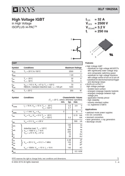
© 2004 IXYS All rights reserved1 - 4407IXYS reserves the right to change limits, test conditions and dimensions.High Voltage IGBTin High Voltage ISOPLUS i4-PAC TMFeatures•High Voltage IGBT-substitute for high voltage MOSFETs with significantly lower voltage drop and comparable switching speed -substitute for high voltage thyristors with voltage control of turn on & turn off - substitute for electromechanical trigger and discharge relays •ISOPLUS i4-PAC TM high voltage package - isolated back surface- enlarged creepage towards heatsink - enlarged creepage between high voltage pins- application friendly pinout - high reliability- industry standard outline - UL registered E 72873Applications•switched mode power supplies •DC-DC converters •resonant converters•laser generators, x ray generators •discharge circuitsI C25= 32 A V CES = 2500 V V CE(sat)= 3.2 V t f= 250 ns512152Symbol Conditions Maximum RatingsV CES T VJ = 25°C to 150°C2500V V GES ± 20V I C25T C = 25°C 32A I C90T C = 90°C19A I CM V GE = ±15 V; R G = 47 Ω; T VJ = 125°C70A V CEK RBSOA, Clamped inductive load; L = 100 µH 1200V P totT C = 25°C 250WSymbol ConditionsCharacteristic Values(T VJ = 25°C, unless otherwise specified)min.typ.max.© 2004 IXYS All rights reserved2 - 4407Dimensions in mm (1 mm = 0.0394")Component Symbol ConditionsMaximum Ratings T VJ -55...+150°C T stg -55...+125°C V ISOL I ISOL ≤ 1 mA; 50/60 Hz 2500V~F Cmounting force with clip 20 (120)NSymbol Conditions Characteristic Values min.typ.max.d S ,d A C pin - E pin7.0mm d S ,d A pin - backside metal 5.5mm R thCH with heatsink compound 0.15K/W Weight9g© 2004 IXYS All rights reserved3 - 440701020304010100100080012345010203040506789101112131415V CEA VV V V GEV CEpF T = 25°CFig. 2Typ. Output CharacteristicsFig. 3Typ. Transfer Characteristics Fig. 4Capacitance curvesFig. 5Typ. Gate Charge characteristicsFig. 6Reverse Biased Safe Operating AreaRBSOA© 2004 IXYS All rights reserved4 - 44070102030405005101520253035E onE on mJV = 1500 V 0.0010.010.11100.010.11ts Z thJCFig. 11Typ. transient thermal impedanceFig. 9Typ. turn on energy and switchingFig. 10Typ. turn off energy and switchingtimes versus gate resistortimes versus gate resistor。
TH-2050-VFM 全功能平板电视墙壁挂件说明书
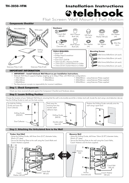
'ULOOLQJ *XLGH
:$//
)5217
'ULOOLQJ *XLGH
%$&.
'XVW &ROOHFWRU
'RXEOHVLGHG WDSH [
Step 3. Attaching the Articulated Arm to the Wall
Timber Stud Wall 8VLQJ WKH 'ULOOLQJ *XLGH GULOO WKUHH PP µ GLDPHWHU KROHV
TILT DOWN
Tighten the Clamp Lever to lock the Display in desired position.
Clamp Lever
PULL TO RESET
LOOSEN
TIP: If the Clamp Lever is obstructed pull it outwards to disengage the rachet mechanism.
0 'RPH 1XW [
&RDFK :DVKHU 0 [
0 :DVKHU [
([WHQVLRQ 3ODWH $ [
'ULOOLQJ *XLGH
([WHQVLRQ 3ODWH % [
$QFKRU &RQFUHWH [
0 6SDFHU %XVK [
6WDU :DVKHU [
Mounting Screws 0[PP0[PP [ HDFK 0[PP0[PP [ HDFK 0[PP0[PP [ HDFK 0[PP0[PP [ HDFK
Hale Waihona Puke IMPORTANT INFORMATION