IPA50R299CP中文资料
blackstar debut 50r使用指南说明书

7. 50W / 5W
Your DEBUT 50R is a 50W amplifier, however you can keep the neighbours happy and push the switch in for a power reduction down to 5W, without sacrificing your tone.
超载增益(Gain)旋钮可以调节超载(失真)的数量. 增益设置更大将会提供更多的超 载声音. 超载音量(Volume)旋钮可以调节超载通道的音量大小。
5. CHOOSE YOUR SOUND
Set your bass, middle and treble and choose anywhere in between a UK and American sound using Blackstar’s patented ISF control.
Écoutez l’audio de votre téléphone, lecteur MP3, tablette ou ordinateur portable via votre DEBUT 50R à l’aide d’un câble auxiliaire stéréo (vendu séparément) - ou jouez “en silence” en branchant un casque sur votre DEBUT 50R via la prise jack LINE OUT / PHONES.
a selectable Plate / Hall reverb, make it the perfect amp for stage or studio.
LP2951-50DR中文资料

• LP2951 Only (8-Pin Package) – Fixed- or Adjustable-Output Voltages: 5 V/ADJ, 3.3 V/ADJ, and 3 V/ADJ
– Low-Voltage Error Signal on Falling Output
ORDERING INFORMATION(1)
TA –40°C to 125°C
VOUT (NOM)
3V
3.3 V
5V ADJ
PACKAGE (2)
TO-226/TO-92 – LP SOIC – D TO-226/TO-92 – LP SOIC – D TO-226/TO-92 – LP SOIC – D SOIC-D
Please be aware that an important notice concerning availability, standard warranty, and use in critical applications of Texas Instruments semiconductor products and disclaimers thereto appears at the end of this data sheet.
– 1.4% at 25°C – 2% Over Temperature • Can Be Used as a Regulator or Reference
• Stable With Low ESR (>12 mΩ) Capacitors • Current- and Thermal-Limiting Features • LP2950 Only (3-Pin Package)
Palo Alto Networks PA-5200系列产品数据手册说明书

Palo Alto Networks | PA-5200 Series | Datasheet1Key Security Features: Classifies all applications, on all ports, all the time • Identifies the application, regardless of port, encryption (SSL or SSH), or evasive technique employed • Uses the application, not the port, as the basis for all of your safe enablement policy decisions: allow, deny, s chedule, inspect and apply traffic-shaping • Categorizes unidentified applications for policy control, threat forensics or App-ID™ application identification technology development Enforces security policies for any user, at any location • Deploys consistent policies to local and remote users running on the Windows ®; Apple ® Mac ® OS X ®, macOS™ and iOS; Linux ®; and Android™ platforms • Enables agentless integration with Microsoft ®A ctive D irectory ® and T erminal Services, LDAP, Novell ® e Directory™ and Citrix ®• Easily integrates your firewall policies with 802.1X w ireless, proxies, NAC solutions, and any other source of user identity information Prevents known and unknown threats • Blocks a range of known threats, including exploits, m alware and spyware, across all ports, regardless ofc ommon threat-evasion tactics employed • Limits the unauthorized transfer of files and sensitive data, and safely enables non-work-related web surfing • Identifies unknown malware, analyzes it based on hundreds of malicious behaviors, and then automatically creates and delivers protection The controlling element of the PA-5200 Series is P AN-OS, security operating system, which that natively classifies all traffic, inclusive of applications, threats and content, and then ties that traffic to the user, regardless of location or device type. The application, content and user – in other words, the elements that run your business – are then used as the basis of your security policies, resulting in an improved security posture and a reduction in incidentresponse time. Palo Alto Networks ® PA-5200 Series of next-generation f irewall a ppliances is c omprised of the PA-5260, the PA-5250 and the P A-5220, which target high-speed data c enter, internet g ateway, and service provider deployments. The P A-5200 Series delivers up to 72 Gbps of throughput using dedicated p rocessing and memory for the key functional areas of n etworking, security,threat prevention and management.PA-5200SERIES 1 Performance and capacities are measured under ideal testing conditions. 2 Firewall throughput measured with App-ID and User-ID features enabled utilizing 64K HTTP transactions 3 Threat prevention throughput measured with App-ID, User-ID, IPS, A ntiVirusand Anti-Spyware features enabled utilizing 64K HTTP transactions 4. New sessions per second is measured with 4K HTTP transactions 5. Adding virtual systems base quantity requires a separately purchased license PA-5260PA-5220PA-52504401 Great America Parkway Santa Clara, CA 95054 Main: +1.408.753.4000 Sales: +1.866.320.4788 Support: +1.866.898.9087 © 2017 Palo Alto Networks, Inc. Palo Alto Networks is a registered trademark of Palo Alto Networks. A list of our trademarks can be found at / company/trademarks.html. All other marks mentioned herein may be trademarks of theirrespective companies. pa-5200-series-ds-020817Networking FeaturesHardware Specifications。
PJP-50R
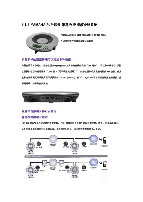
1.1.1 YAMAHA PJP-50R 雅马哈IP音频会议系统
内置式LAN端口.LINE端口.AUDIO IN/OUT端口,
可以使用多种用途的音频会议系统
多种多样的连接终端可以对应各种场面
内置安装了3个端口。
能够实现projectphone之间的高音质会议的“LAN端口”。
可以和一般电话.手机以及模拟电话终端通话的“LINE端口(用于模拟电话线)”。
能够实现和个人电脑连接的Web会议,作为软件电话的麦克风兼扬声器可以使用的“AUDIO (IN/OUT) 端口”。
PJP-50R可以对应各种用途的需要,是多用途端口的音频会议系统。
内置式音频混合器可以利用
各种线路的混合通话
PJP-50R有内置式各种式样的连接终端,“IP 模拟电话+音频”可以同事连接,通话。
IP电话会议中,从外出地点用手机也可以参加会议,也可以使用电话,只用声音直接参加Web会议。
多数人的会议也可以“易听”
再现说话人的位置
麦克风阵列的说话人位置检测功能和扬声器阵列的虚拟音源生成功能的组合,可以把通话地点的座位位置相吻合的声音再现出来,实现了“说话人位置再现模式”。
从不同的位置的声音能准确的再现播放出,及时有多人的发言也能简单地分辨听清(IP2地点通话时,最多有3个说话人位置)
规格:。
贝加莱50点壁厚控制器说明书330
PP41型壁厚控制器使用说明书贝加莱工业自动化(上海)有限公司目录系统特性简介 (3)1系统特性介绍 (3)2控制系统各部件介绍 (4)2.1控制操作面板 (4)2.1.1 面板 42.1.2 接口 52.1.3 性能 62.1.4 安装 62.2功能按键及指示灯 (7)2.3控制器及接线 (9)2.3.1AI351 (9)2.3.2 Am351 (10)2.3.3 PP41自带输入 (10)2.3.4 PP41自带输出 (11)3画面操作说明 (12)3.1登陆画面 (12)3.2连续式型胚曲线设定画面 (12)3.2.1 操作按钮 (12)3.2.2 输入参数 (13)3.2.3 输出参数 (14)3.2.4 插入与删除设定数值点 (14)3.2.5 微调设定数值点间的曲线单元 (15)3.3储料式型胚曲线设定画面 (17)3.3.1 操作按钮 (17)3.3.2 输入参数 (18)3.3.3 输出参数 (19)3.4曲线跟踪画面 (19)3.5标记画面 (20)3.6存储画面 (20)3.7文件改名画面 (21)3.8参数存储画面 (21)3.9文件调出画面 (22)3.10监控画面 (22)3.11数据1(曲线点)画面 (22)3.12数据2画面 (23)3.13初始设定画面 (23)3.13.1 输入参数 (23)3.13.2 模式转换 (24)3.14型芯设定画面 (24)3.14.1 输入参数 (24)3.14.2 输出参数 (25)3.14.3 手动调校 (25)3.14.4 自动调校 (25)3.14.5 调校提示: (25)3.15储料设定画面 (26)3.15.1 输出参数 (26)3.15.2 手动调校 (26)3.16增益设定画面 (26)3.16.1 按钮 273.16.2 输入参数 (27)3.16.3 输出参数 (27)3.17时间设定画面 (27)3.17.1 输入参数 (27)3.17.2 输出参数 (27)3.18中英文切换画面 (28)4机器操作说明 (29)4.1开机步骤 (29)4.2系统参数设定 (29)4.2.1 初始设定 (29)4.2.2 型芯设定 (29)4.2.3 储料设定 (29)5故障处理 (30)5.1故障对应 (30)5.2干扰处理 (30)6电源 (30)7附件 (30)系统特性简介1 系统特性介绍这是一款50点型坯壁厚控制器,用来控制中空成型机型坯的壁厚。
atc中文手册
A T24C256中文资料2009-11-15 09:43特性???? 与1MHz I2C 总线兼容???? 到伏工作电压范围???? 低功耗CMOS 技术???? 写保护功能当WP 为高电平时进入写保护状态???? 64 字节页写缓冲器???? 自定时擦写周期???? 100,000 编程/擦写周期???? 可保存数据100 年???? 8 脚DIP SOIC 封装???? 温度范围商业级工业级和汽车级概述CAT24WC256 是一个256K 位串行CMOS E2PROM 内部含有32768 个字节每字节为8 位CATALYST 公司的先进CMOS 技术实质上减少了器件的功耗CAT24WC256 有一个64 字节页写缓冲器该器件通过I2C 总线接口进行操作管脚描述管脚名称功能A0 A1 地址输入SDA 串行数据/地址SCL 串行时钟WP 写保护Vcc + 电源Vss 地NC 未连接极限参数工作温度工业级-55 +125商业级0 +75贮存温度-65 +150各管脚承受电压 Vcc+Vcc 管脚承受电压 +封装功率损耗Ta=25焊接温度(10 秒) 300口输出短路电流100mA功能描述CAT24WC256 支持I2C 总线数据传送协议I2C 总线协议规定任何将数据传送到总线的器件作为发送器任何从总线接收数据的器件为接收器数据传送是由产生串行时钟和所有起始停止信号的主器件控制的CAT24WC256 是作为从器件被操作的主器件和从器件都可以作为发送器或接收器但由主器件控制传送数据发送或接收的模式管脚描述SCL 串行时钟CAT24WC256 串行时钟输入管脚用于产生器件所有数据发送或接收的时钟这是一个输入管脚SDA 串行数据/地址双向串行数据/地址管脚用于器件所有数据的发送或接收SDA 是一个开漏输出管脚可与其它开漏输出或集电极开路输出进行线或wire-ORWP 写保护当WP 脚连接到Vcc 所有内存变成写保护只能读当WP 引脚连接到Vss 或悬空允许器件进行读/写操作A0 A1 器件地址输入这些管脚为硬连线或者不连接对于单总线系统最多可寻址4 个CAT24WC256 器件参阅器件寻址当这些引脚没有连接时其默认值为0I2C 总线协议I2C 总线协议定义如下1 只有在总线空闲时才允许启动数据传送2 在数据传送过程中当时钟线为高电平时数据线必须保持稳定状态不允许有跳变时钟线为高电平时数据线的任何电平变化将被看作总线的起始或停止信号起始信号时钟线保持高电平期间数据线电平从高到低的跳变作为I2C 总线的起始信号停止信号时钟线保持高电平期间数据线电平从低到高的跳变作为I2C 总线的停止信号器件寻址主器件通过发送一个起始信号启动发送过程然后发送它所要寻址的从器件的地址8 位从器件地址的高5 位固定为10100 见图5 接下来的2 位A1 A0 为器件的地址位最多可以连接4 个器件到同一总线上这些位必须与硬连线输入脚A1 A0 相对应从器件地址的最低位作为读写控制位1表示对从器件进行读操作0 表示对从器件进行写操作在主器件发送起始信号和从器件地址字节后CAT24WC256 监视总线并当其地址与发送的从地址相符时响应一个应答信号通过SDA 线CAT24WC256 再根据读写控制位R/W 的状态进行读或写操作应答信号I2C 总线数据传送时每成功地传送一个字节数据后接收器都必须产生一个应答信号应答的器件在第9 个时钟周期时将SDA 线拉低表示其已收到一个8 位数据CAT24WC256 在接收到起始信号和从器件地址之后响应一个应答信号如果器件已选择了写操作则在每接收一个8 位字节之后响应一个应答信号当CAT24WC256 工作于读模式时在发送一个8 位数据后释放SDA 线并监视一个应答信号一旦接收到应答信号CAT24WC256 继续发送数据如主器件没有发送应答信号器件停止传送数据并等待一个停止信号写操作字节写在字节写模式下主器件发送起始信号和从器件地址信息R/W 位置0 给从器件在从器件送回应答信号后主器件发送两个8 位地址字写入CAT24WC256 的地址指针主器件在收到从器件的应答信号后再发送数据到被寻址的存储单元CAT24WC256 再次应答并在主器件产生停止信号后开始内部数据的擦写在内部擦写过程中CAT24WC256 不再应答主器件的任何请求页写在页写模式下单个写周期内CAT24WC256 最多可以写入64 个字节数据页写操作的启动和字节写一样不同在于传送了一字节数据后主器件允许继续发送63 个字节每发送一个字节后CAT24WC256 将响应一个应答位且内部低6 位地址加1 高位地址保持不变如果主器件在发送停止信号之前发送大于64 个字节地址计数器将自动翻转先前写入的数据被覆盖当所有64 字节接收完毕主器件发送停止信号内部编程周期开始此时所有接收到的数据在单个写周期内写入CAT24WC256应答查询可以利用内部写周期时禁止数据输入这一特性一旦主器件发送停止位指示主器件操作结束时CAT24WC256 启动内部写周期应答查询立即启动包括发送一个起始信号和进行写操作的从器件地址如果CAT24WC256 正在进行内部写操作将不会发送应答信号如果CAT24WC256 已经完成了内部写操作将发送一个应答信号主器件可以继续对CAT24WC256 进行下一次读写操作写保护写保护操作特性可使用户避免由于不当操作而造成对存储区域内部数据的改写当WP 管脚接高时整个寄存器区全部被保护起来而变为只可读取CAT24WC256 可以接收从器件地址和字节地址但是装置在接收到第一个数据字节后不发送应答信号从而避免寄存器区域被编程改写读操作CAT24WC256 读操作的初始化方式和写操作时一样仅把R/W 位置为1 有三种不同的读操作方式立即/当前地址读选择/随机读和连续读立即/当前地址读的地址计数器内容为最后操作字节的地址加1 也就是说如果上次读/写的操作地址为N 则立即读的地址从地址N+1 开始如果N=E 此处E=32767 则计数器将翻转到0 且继续输出数据CAT24WC256接收到从器件地址信号后R/W 位置1 它首先发送一个应答信号然后发送一个8 位字节数据主器件不需发送一个应答信号但要产生一个停止信号选择/随机读选择/随机读操作允许主器件对寄存器的任意字节进行读操作主器件首先通过发送起始信号从器件地址和它想读取的字节数据的地址执行一个伪写操作在CAT24WC256 应答之后主器件重新发送起始信号和从器件地址此时R/W 位置1 CAT24WC256 响应并发送应答信号然后输出所要求的一个8 位字节数据主器件不发送应答信号但产生一个停止信号连续读连续读操作可通过立即读或选择性读操作启动在CAT24WC256 发送完一个8 位字节数据后主器件产生一个应答信号来响应告知CAT24WC256 主器件要求更多的数据对应每个主机产生的应答信号CAT24WC256 将发送一个8 位数据字节当主器件不发送应答信号而发送停止位时结束此操作从CAT24WC256 输出的数据按顺序由N 到N+1 输出读操作时地址计数器在CAT24WC256 整个地址内增加这样整个寄存器区域在可在一个读操作内全部读出当读取的字节超过E 此处E=32767计数器将翻转到零并继续输出数据字节。
LP2992_DataSheet

LP2992Micropower 250mA Low-Noise Ultra Low-Dropout Regulator in SOT-23and LLP PackagesDesigned for Use with Very Low ESR Output CapacitorsGeneral DescriptionThe LP2992is a 250mA,fixed-output voltage regulator designed to provide ultra low-dropout and low noise in bat-tery powered applications.Using an optimized VIP ™(Vertically Integrated PNP)pro-cess,the LP2992delivers unequalled performance in all specifications critical to battery-powered designs:Dropout Voltage:Typically 450mV @250mA load,and 5mV @1mA load.Ground Pin Current:Typically 1500µA @250mA load,and 75µA @1mA load.Enhanced Stability:The LP2992is stable with output ca-pacitor ESR as low as 5m Ω,which allows the use of ceramic capacitors on the output.Sleep Mode:Less than 1µA quiescent current when ON/OFF pin is pulled low.Smallest Possible Size:SOT-23and LLP packages use absolute minimum board space.Precision Output:1%tolerance output voltages available (A grade).Low Noise:By adding a 10nF bypass capacitor,output noise can be reduced to 30µV (typical).Multiple voltage options,from 1.5V to 5.0V,are available as standard products.Consult factory for custom voltages.Featuresn Ultra low dropout voltagen Guaranteed 250mA output currentn Smallest possible size (SOT-23,LLP package)n Requires minimum external components n Stable with low-ESR output capacitor n <1µA quiescent current when shut down n Low ground pin current at all loads n Output voltage accuracy 1%(A Grade)n High peak current capabilityn Wide supply voltage range (16V max)n Low Z OUT :0.3Ωtypical (10Hz to 1MHz)n Overtemperature/overcurrent protectionn −40˚C to +125˚C junction temperature range nCustom voltages availableApplicationsn Cellular Phonen Palmtop/Laptop Computern Personal Digital Assistant (PDA)nCamcorder,Personal Stereo,CameraBlock Diagram20029401VIP ™is a trademark of National Semiconductor Corporation.June 2002LP2992Micropower 250mA Low-Noise Ultra Low-Dropout Regulator in SOT-23and LLP Packages©2002National Semiconductor Corporation Basic Application Circuit20029402 *ON/OFF input must be actively terminated.Tie to V IN if this function is not to be used.**Minimum capacitance is shown to ensure stability(may be increased without limit).Ceramic capacitor required for output(see Application Hints).***Reduces output noise(may be omitted if application is not noise critical).Use ceramic or film type with very low leakage current(see Application Hints).Connection Diagrams5-Lead Small Outline Package(M5)6-Lead LLP Package(LD)2Ordering InformationTABLE1.Package Marking and Ordering InformationOutput Voltage(V)Grade Order InformationPackageMarkingSupplied as:5-Lead Small Outline Package(M5)1.5A LP2992AIM5X-1.5LFBA3000Units on Tape and Reel1.5A LP2992AIM5-1.5LFBA1000Units on Tape and Reel1.5STD LP2992IM5X-1.5LFBB3000Units on Tape and Reel1.5STD LP2992IM5-1.5LFBB1000Units on Tape and Reel1.8A LP2992AIM5X-1.8LFCA3000Units on Tape and Reel1.8A LP2992AIM5-1.8LFCA1000Units on Tape and Reel1.8STD LP2992IM5X-1.8LFCB3000Units on Tape and Reel1.8STD LP2992IM5-1.8LFCB1000Units on Tape and Reel2.5A LP2992AIM5X-2.5LFDA3000Units on Tape and Reel2.5A LP2992AIM5-2.5LFDA1000Units on Tape and Reel2.5STD LP2992IM5X-2.5LFDB3000Units on Tape and Reel2.5STD LP2992IM5-2.5LFDB1000Units on Tape and Reel3.0A LP2992AIM5X-3.0LF8A3000Units on Tape and Reel3.0A LP2992AIM5-3.0LF8A1000Units on Tape and Reel3.0STD LP2992IM5X-3.0LF8B3000Units on Tape and Reel3.0STD LP2992IM5-3.0LF8B1000Units on Tape and Reel3.3A LP2992AIM5X-3.3LFEA3000Units on Tape and Reel3.3A LP2992AIM5-3.3LFEA1000Units on Tape and Reel3.3STD LP2992IM5X-3.3LFEB3000Units on Tape and Reel3.3STD LP2992IM5-3.3LFEB1000Units on Tape and Reel5.0A LP2992AIM5X-5.0LFFA3000Units on Tape and Reel5.0A LP2992AIM5-5.0LFFA1000Units on Tape and Reel5.0STD LP2992IM5X-5.0LFFB3000Units on Tape and Reel5.0STD LP2992IM5-5.0LFFB1000Units on Tape and Reel6-Lead LLP Package(LDE06A)1.5A LP2992AILDX-1.5L011A4500Units on Tape and Reel1.5A LP2992AILD-1.5L011A1000Units on Tape and Reel1.5STD LP2992ILDX-1.5L011AB4500Units on Tape and Reel1.5STD LP2992ILD-1.5L011AB1000Units on Tape and Reel1.8A LP2992AILDX-1.8L012A4500Units on Tape and Reel1.8A LP2992AILD-1.8L012A1000Units on Tape and Reel1.8STD LP2992ILDX-1.8L012AB4500Units on Tape and Reel1.8STD LP2992ILD-1.8L012AB1000Units on Tape and Reel2.5A LP2992AILDX-2.5L013A4500Units on Tape and Reel2.5A LP2992AILD-2.5L013A1000Units on Tape and Reel2.5STD LP2992ILDX-2.5L013AB4500Units on Tape and Reel2.5STD LP2992ILD-2.5L013AB1000Units on Tape and Reel3.3A LP2992AILDX-3.3L014A4500Units on Tape and Reel3.3A LP2992AILD-3.3L014A1000Units on Tape and Reel3.3STD LP2992ILDX-3.3L014AB4500Units on Tape and Reel3.3STD LP2992ILD-3.3L014AB1000Units on Tape and Reel5.0A LP2992AILDX-5.0L015A4500Units on Tape and Reel5.0A LP2992AILD-5.0L015A1000Units on Tape and Reel5.0STD LP2992ILDX-5.0L015AB4500Units on Tape and Reel5.0STD LP2992ILD-5.0L015AB1000Units on Tape and ReelLP29923Absolute Maximum Ratings(Note 1)If Military/Aerospace specified devices are required,please contact the National Semiconductor Sales Office/Distributors for availability and specifications.Storage Temperature Range −65˚C to +150˚C Operating Junction Temperature Range−40˚C to +125˚CLead Temp.(Soldering,5sec.)260˚C ESD Rating (Note 2)2kVPower Dissipation (Note 3)Internally LimitedInput Supply Voltage (Survival)−0.3V to +16V Input Supply Voltage (Operating) 2.2V to +16V Shutdown Input Voltage (Survival)−0.3V to +16V Output Voltage (Survival,(Note 4))−0.3V to +9V I OUT (Survival)Short Circuit Protected Input-Output Voltage (Survival,−0.3V to +16V(Note 5))Electrical CharacteristicsLimits in standard typeface are for T J =25˚C.and limits in boldface type apply over the full operating temperature range.Un-less otherwise specified:V IN =V O (NOM)+1V,I L =1mA,C IN =1µF,C OUT =4.7µF,V ON/OFF =2V.Symbol Parameter ConditionsTyp LP2992AI-X.XLP2992I-X.X Units(Note 6)(Note 6)Min Max Min Max ∆V OOutput Voltage ToleranceI L =1mA−1.0 1.0−1.5 1.5%V NOM 1mA ≤I L ≤50mA −1.5 1.5−2.5 2.5−2.5 2.5−3.5 3.51mA ≤I L ≤250mA−3.5 3.5−4.0 4.0−4.54.5−5.05.0Output Voltage V O (NOM)+1V ≤V IN ≤16V 0.0070.0140.014%/VLine Regulation0.0320.032V IN (min)Minimum input voltage required to maintain outpout regulation 2.05 2.202.20V V IN –V ODropout Voltage (Note 7)I L =00.5 2.5 2.5mV44I L =1mA 5991212I L =50mA 100125125180180I L =150mA 260325325470470I L =250mA450575575850850I GNDGround Pin CurrentI L =0659595µA 125125I L =1mA 75110110170170I L =50mA 35060060010001000I L =150mA 8501500150025002500I L =250mA 15002300230040004000V ON/OFF <0.3V 0.010.80.8V ON/OFF <0.15V0.0522V ON/OFFON/OFF Input Voltage (Note 8)High =O/P ON 1.4 1.61.6V Low =O/P OFF0.550.150.15L P 29924Electrical Characteristics(Continued)Limits in standard typeface are for T J =25˚C.and limits in boldface type apply over the full operating temperature range.Un-less otherwise specified:V IN =V O (NOM)+1V,I L =1mA,C IN =1µF,C OUT =4.7µF,V ON/OFF =2V.SymbolParameter ConditionsTyp LP2992AI-X.XLP2992I-X.X Units(Note 6)(Note 6)MinMax MinMax I ON/OFF ON/OFF Input Current V ON/OFF =00.01−2−2µA V ON/OFF =5V51515e nOutput Noise BW =300Hz to 50kHz,Voltage (RMS)C OUT =10µF 30µVC BYPASS =10nFRipple Rejectionf =1kHz,C BYPASS =10nF 45dB C OUT =10µFI O (SC)Short Circuit Current R L =0(Steady State)400mA (Note 9)I O (PK)Peak Output CurrentV OUT ≥V o (NOM)−5%350mANote 1:“Absolute Maximum Ratings”indicate limits beyond which damage to the component may occur.Electrical specifications do not apply when operating the device outside of its rated operating conditions.Note 2:The ESD rating of pins 3and 4for the SOT-23package,or pins 1and 3for the LLP package,is 1kV.Note 3:The maximum allowable power dissipation is a function of the maximum junction temperature,T J (MAX),the junction-to-ambient thermal resistance,θJ-A ,and the ambient temperature,T A .The maximum allowable power dissipation at any ambient temperture is calculated using:Where the value of θJ-A for the SOT-23package is 220˚C/W in a typical PC board mounting and the LLP package is 65˚C/W.Exceeding the maximum allowable dissipation will cause excessive die temperature,and the regulator will go into thermal shutdown.Note 4:If used in a dual-supply system where the regulator load is returned to a negative supply,the LP2992output must be diode-clamped to ground.Note 5:The output PNP structure contains a diode between the V IN to V OUT terminals that is normally reverse-biased.Reversing the polarity from V IN to V OUT will turn on this diode.Note 6:Limits are 100%production tested at 25˚C.Limits over the operating temperature range are guaranteed through correlation using Statistical Quality Control (SQC)methods.The limits are used to calculate National’s Average Outgoing Quality Level (AOQL).Note 7:V IN must be the greater of 2.2V or V OUT(nom)+Dropout Voltage to maintain output regulation.Dropout voltage is defined as the input to output differential at which the output voltage drops 2%below the value measured with a 1V differential.Note 8:The ON/OFF input must be properly driven to prevent possible misoperation.For details,refer to Application Hints.Note 9:The LP2992has foldback current limiting which allows a high peak current when V OUT >0.5V,and then reduces the maximum output current as V OUT is forced to ground (see Typical Performance Characteristics curves).LP29925Typical Performance CharacteristicsUnless otherwise specified:C IN =1µF,C OUT =4.7µF,V IN =V OUT (NOM)+1,T A =25˚C,ON/OFF pin is tied to V IN .V OUT vs TemperatureShort-Circuit Current2002940820029409Short-Circuit Current Short Circuit Current vs Output Voltage2002941020029411Ripple Rejection Ripple Rejection2002941320029414L P 2992 6Typical Performance Characteristics Unless otherwise specified:C IN =1µF,C OUT =4.7µF,V IN =V OUT (NOM)+1,T A =25˚C,ON/OFF pin is tied to V IN .(Continued)Ripple RejectionRipple Rejection2002941520029416Ripple Rejection Ripple Rejection2002941720029418Ripple Rejection Ripple Rejection2002941920029423LP29927Typical Performance Characteristics Unless otherwise specified:C IN =1µF,C OUT =4.7µF,V IN =V OUT (NOM)+1,T A =25˚C,ON/OFF pin is tied to V IN .(Continued)Ripple RejectionOutput Impedance vs Frequency2002942220029420Output Impedance vs Frequency Output Noise Density2002942120029424Output Noise Density GND Pin vs Load Current2002942520029426L P 2992 8Typical Performance Characteristics Unless otherwise specified:C IN =1µF,C OUT =4.7µF,V IN =V OUT (NOM)+1,T A =25˚C,ON/OFF pin is tied to V IN .(Continued)Dropout Voltage vs Temperature Input Current vs Pin2002942720029429Ignd vs Load and Temperature Instantaneous Short Circuit Current2002943020029431Load Transient Response Load Transient Response20029434LP29929Typical Performance Characteristics Unless otherwise specified:C IN =1µF,C OUT =4.7µF,V IN =V OUT (NOM)+1,T A =25˚C,ON/OFF pin is tied to V IN .(Continued)Load Transient Response Line Transient Response2002944720029435Line Transient Response Line Transient Response2002943620029437Line Transient Response Turn-On Time2002943820029439L P 2992 10Typical Performance Characteristics Unless otherwise specified:C IN =1µF,C OUT =4.7µF,V IN =V OUT (NOM)+1,T A =25˚C,ON/OFF pin is tied to V IN .(Continued)Turn-On TimeTurn-On Time2002944020029441Turn-On Time20029442LP299211Application HintsEXTERNAL CAPACITORSLike any low-dropout regulator,the LP2992requires external capacitors for regulator stability.These capacitors must be correctly selected for good performance.Input CapacitorAn input capacitor whose capacitance is ≥1µF is required between the LP2992input and ground (the amount of ca-pacitance may be increased without limit).This capacitor must be located a distance of not more than 1cm from the input pin and returned to a clean analog ground.Any good quality ceramic,tantalum,or film capacitor may be used at the input.Important:Tantalum capacitors can suffer catastrophic fail-ure due to surge current when connected to a low-impedance source of power (like a battery or very large capacitor).If a Tantalum capacitor is used at the input,it must be guaranteed by the manufacturer to have a surge current rating sufficient for the application.There are no requirements for ESR on the input capacitor,but tolerance and temperature coefficient must be consid-ered when selecting the capacitor to ensure the capacitance will be ≥1µF over the entire operating temperature range.Output Capacitor:The LP2992is designed specifically to work with ceramic output capacitors,utilizing circuitry which allows the regula-tor to be stable across the entire range of output current with an output capacitor whose ESR is as low as 5m Ω.It may also be possible to use Tantalum or film capacitors at the output,but these are not as attractive for reasons of size and cost (see next section Capacitor Characteristics).The output capacitor must meet the requirement for mini-mum amount of capacitance and also have an ESR (equiva-lent series resistance)value which is within the stable range.Curves are provided which show the stable ESR range as a function of load current (see ESR graph below).20029407Important:The output capacitor must maintain its ESR within the stable region over the full operating temperature range of the application to assure stability.The LP2992requires a minimum of 4.7µF on the output (output capacitor size can be increased without limit).It is important to remember that capacitor tolerance and variation with temperature must be taken into consideration when selecting an output capacitor so that the minimum required amount of output capacitance is provided over the full operating temperature range.It should be noted thatceramic capacitors can exhibit large changes in capacitance with temperature (see next section,Capacitor Characteris-tics ).The output capacitor must be located not more than 1cm from the output pin and returned to a clean analog ground.Noise Bypass Capacitor:Connecting a 10nF capacitor to the Bypass pin significantly reduces noise on the regulator output.It should be noted that the capacitor is connected directly to a high-impedance cir-cuit in the bandgap reference.Because this circuit has only a few microamperes flowing in it,any significant loading on this node will cause a change in the regulated output voltage.For this reason,DC leakage current through the noise bypass capacitor must never ex-ceed 100nA,and should be kept as low as possible for best output voltage accuracy.The types of capacitors best suited for the noise bypass capacitor are ceramic and film.High-quality ceramic capaci-tors with either NPO or COG dielectric typically have very low leakage.10nF polypropolene and polycarbonate film capacitors are available in small surface-mount packages and typically have extremely low leakage current.CAPACITOR CHARACTERISTICSThe LP2992was designed to work with ceramic capacitors on the output to take advantage of the benefits they offer:for capacitance values in the 2.2µF to 10µF range,ceramics are the least expensive and also have the lowest ESR values (which makes them best for eliminating high-frequency noise).The ESR of a typical 4.7µF ceramic capacitor is in the range of 5m Ωto 10m Ω,which easily meets the ESR limits required for stability by the LP2992.One disadvantage of ceramic capacitors is that their capaci-tance can vary with temperature.Most large value ceramic capacitors (≥2.2µF)are manufactured with the Z5U or Y5V temperature characteristic,which results in the capacitance dropping by more than 50%as the temperature goes from 25˚C to 85˚C.This could cause problems if a 4.7µF capacitor were used on the output since it will drop down to approximately 2.3µF at high ambient temperatures (which could cause the LP2992to oscillate).If Z5U or Y5V capacitors are used on the output,a minimum capacitance value of 10µF must be observed.A better choice for temperature coefficient in ceramic capaci-tors is X7R,which holds the capacitance within ±15%.Un-fortunately,the larger values of capacitance are not offered by all manufacturers in the X7R dielectric.Tantalum:Tantalum capacitors are less desirable than ceramics for use as output capacitors because they are more expensive when comparing equivalent capacitance and voltage ratings in the 1µF to 4.7µF range.Another important consideration is that Tantalum capacitors have higher ESR values than equivalent size ceramics.This means that while it may be possible to find a Tantalum capacitor with an ESR value within the stable range,it would have to be larger in capacitance (which means bigger and more costly)than a ceramic capacitor with the same ESR value.L P 2992 12Application Hints(Continued)It should also be noted that the ESR of a typical Tantalum will increase about2:1as the temperature goes from25˚C down to−40˚C,so some guard band must be allowed.ON/OFF INPUT OPERATIONThe LP2992is shut off by driving the ON/OFF input low,and turned on by pulling it high.If this feature is not to be used, the ON/OFF input should be tied to V IN to keep the regulator output on at all times.To assure proper operation,the signal source used to drive the ON/OFF input must be able to swing above and below the specified turn-on/turn-off voltage thresholds listed in the Electrical Characteristics section under V ON/OFF.To prevent mis-operation,the turn-on(and turn-off)voltage signals ap-plied to the ON/OFF input must have a slew rate which is ≥40mV/µs.Caution:the regulator output voltage can not be guaranteed if a slow-moving AC(or DC)signal is applied that is in the range between the specified turn-on and turn-off voltages listed under the electrical specification V ON/OFF(see Electri-cal Characteristics).REVERSE INPUT-OUTPUT VOLTAGEThe PNP power transistor used as the pass element in the LP2992has an inherent diode connected between the regu-lator output and input.During normal operation(where the input voltage is higher than the output)this diode is reverse-biased.However,if the output is pulled above the input,this diodewill turn ON and current will flow into the regulator output.Insuch cases,a parasitic SCR can latch which will allow a highcurrent to flow into V IN(and out the ground pin),which candamage the part.In any application where the output may be pulled above theinput,an external Schottky diode must be connected fromV IN to V OUT(cathode on V IN,anode on V OUT),to limit thereverse voltage across the LP2992to0.3V(see AbsoluteMaximum Ratings).LLP MountingThe LLP package requires specific mounting techniqueswhich are detailed in National Semiconductor ApplicationNote#1187.Referring to the section PCB Design Recom-mendations,it should be noted that the pad style whichshould be used with the LLP package is the NSMD(non-solder mask defined)type.LP299213Physical Dimensionsinches (millimeters)unless otherwise noted5-Lead Small Outline Package (M5)NS Package Number MF05AFor Order Numbers,refer to Table 1in the “Ordering Information”section of this document.L P 2992 14Physical Dimensionsinches (millimeters)unless otherwise noted (Continued)6-Lead LLP Package (LD)NS Package Number LDE06ALIFE SUPPORT POLICYNATIONAL’S PRODUCTS ARE NOT AUTHORIZED FOR USE AS CRITICAL COMPONENTS IN LIFE SUPPORT DEVICES OR SYSTEMS WITHOUT THE EXPRESS WRITTEN APPROVAL OF THE PRESIDENT AND GENERAL COUNSEL OF NATIONAL SEMICONDUCTOR CORPORATION.As used herein:1.Life support devices or systems are devices or systems which,(a)are intended for surgical implant into the body,or (b)support or sustain life,and whose failure to perform when properly used in accordance with instructions for use provided in the labeling,can be reasonably expected to result in a significant injury to the user.2.A critical component is any component of a life support device or system whose failure to perform can be reasonably expected to cause the failure of the life support device or system,or to affect its safety or effectiveness.National Semiconductor Corporation AmericasEmail:support@National Semiconductor EuropeFax:+49(0)180-5308586Email:europe.support@Deutsch Tel:+49(0)6995086208English Tel:+44(0)8702402171Français Tel:+33(0)141918790National Semiconductor Asia Pacific Customer Response Group Tel:65-2544466Fax:65-2504466Email:ap.support@National Semiconductor Japan Ltd.Tel:81-3-5639-7560Fax:81-3-5639-7507LP2992Micropower 250mA Low-Noise Ultra Low-Dropout Regulator in SOT-23and LLP PackagesNational does not assume any responsibility for use of any circuitry described,no circuit patent licenses are implied and National reserves the right at any time without notice to change said circuitry and specifications.。
罗克韦尔 Compact 5000 I O 数字量模块 说明书
基于 EtherNet/IP 的连接 . . . . . . . . . . . . . . . . . . . . . . . . . . . . . . . . . . . 56 使用 External Means 时连接的其他注意事项 . . . . . . . . . . . . . . . . 57 受限操作 . . . . . . . . . . . . . . . . . . . . . . . . . . . . . . . . . . . . . . . . . . . . . . . . . . . . . . . 58 安全模块特定注意事项 . . . . . . . . . . . . . . . . . . . . . . . . . . . . . . . . . . . . . . . . 59 整体系统安全功能 . . . . . . . . . . . . . . . . . . . . . . . . . . . . . . . . . . . . . . . . . 60 单通道或双通道模式 . . . . . . . . . . . . . . . . . . . . . . . . . . . . . . . . . . . . . . . 60 与安全控制器结合使用 . . . . . . . . . . . . . . . . . . . . . . . . . . . . . . . . . . . . 61 确定符合性 . . . . . . . . . . . . . . . . . . . . . . . . . . . . . . . . . . . . . . . . . . . . . . . . 61
- 1、下载文档前请自行甄别文档内容的完整性,平台不提供额外的编辑、内容补充、找答案等附加服务。
- 2、"仅部分预览"的文档,不可在线预览部分如存在完整性等问题,可反馈申请退款(可完整预览的文档不适用该条件!)。
- 3、如文档侵犯您的权益,请联系客服反馈,我们会尽快为您处理(人工客服工作时间:9:00-18:30)。
UnitIPA50R299CPMaximum ratings, at T j =25 °C, unless otherwise specified ParameterSymbol Conditions Unit Continuous diode forward current 1)I S ADiode pulse current2)I S,pulse 26Reverse diode d v /d t 4)d v /d t15V/nsParameter Symbol ConditionsUnitmin.typ.max.Thermal characteristicsThermal resistance, junction - case R thJC -- 1.2K/WR thJA leaded--62Soldering temperature,wavesoldering only allowed at leadsT sold1.6 mm (0.063 in.) from case for 10 s--260°C Electrical characteristics, at T j =25 °C, unless otherwise specified Static characteristicsDrain-source breakdown voltage V (BR)DSS V GS =0 V, I D =250 µA 500--VGate threshold voltageV GS(th)V DS =V GS , I D =0.44 mA 2.533.5Zero gate voltage drain current I DSS V DS =500 V, V GS =0 V, T j =25 °C--1µAV DS =500 V, V GS =0 V, T j =150 °C-10-Gate-source leakage current I GSS V GS =20 V, V DS =0 V --100nA Drain-source on-state resistanceR DS(on)V GS =10 V, I D =6.6 A, T j =25 °C-0.270.299ΩV GS =10 V, I D =6.6 A, T j =150 °C-0.68-Gate resistanceR Gf =1 MHz, open drain-2.2-ΩValues Thermal resistance, junction - ambientValue T C =25 °C6.6IPA50R299CPParameterSymbol ConditionsUnitmin.typ.max.Dynamic characteristics Input capacitance C iss -1190-pFOutput capacitanceC oss-53-Effective output capacitance, energyrelated 5)C o(er)-50-Effective output capacitance, time related 6)C o(tr)-110-Turn-on delay time t d(on)-35-nsRise timet r -14-Turn-off delay time t d(off)-80-Fall timet f-12-Gate Charge Characteristics Gate to source charge Q gs -5-nCGate to drain charge Q gd -7-Gate charge total Q g -2331Gate plateau voltage V plateau-5.2-VReverse Diode Diode forward voltage V SD V GS =0 V, I F =6.6 A, T j =25 °C-0.9 1.2V Reverse recovery time t rr -260-ns Reverse recovery charge Q rr - 2.6-µC Peak reverse recovery currentI rrm-21-A0) J-STD20 and JESD221) Limited only by T j,max2) Pulse width t p limited by T j,max3) Repetitive avalanche causes additional power losses that can be calculated as P AV =E AR *f.6)C o(tr) is a fixed capacitance that gives the same charging time as C oss while V DS is rising from 0 to 80% V DSS.4) I SD ≤I D , d i /d t ≤200A/µs, V DClink =400V, V peak <V (BR)DSS , T j <T jmax , identical low and high side switchV R =400 V, I F =I S , d i F /d t =100 A/µs5) C o(er) is a fixed capacitance that gives the same stored energy as C oss while V DS is rising from 0 to 80% V DSS.Values V GS =0 V, V DS =100 V, f =1 MHzV DD =400 V,V GS =10 V, I D =6.6 A, R G =27.9 ΩV DD =400 V, I D =6.6 A, V GS =0 to 10 VV GS =0 V, V DS =0 V to 400 V1 Power dissipation5 Typ. output characteristics9 Typ. gate charge13 Typ. capacitancesIPA50R299CP Definition of diode switching characteristicsIPA50R299CP PG-TO220-3-31;-3-111: Outline / Fully isolated package ( 2500VAC; 1minute )IPA50R299CPPublished byInfineon Technologies AG81726 Munich, Germany© 2007 Infineon Technologies AGAll Rights Reserved.Legal DisclaimerThe information given in this document shall in no event be regarded as a guarantee ofconditions or characteristics. With respect to any examples or hints given herein, any typicalvalues stated herein and/or any information regarding the application of the device,Infineon Technologies hereby disclaims any and all warranties and liabilities of any kind,including without limitation, warranties of non-infringement of intellectual property rightsof any third party.InformationFor further information on technology, delivery terms and conditions and prices, pleasecontact the nearest Infineon Technologies Office().WarningsDue to technical requirements, components may contain dangerous substances. For informationon the types in question, please contact the nearest Infineon Technologies Office.Infineon Technologies components may be used in life-support devices or systems only withthe express written approval of Infineon Technologies, if a failure of such components canreasonably be expected to cause the failure of that life-support device or system or to affectthe safety or effectiveness of that device or system. Life support devices or systems areintended to be implanted in the human body or to support and/or maintain and sustainand/or protect human life. If they fail, it is reasonable to assume that the health of the useror other persons may be endangered.。