NSR05F40NXT5G;中文规格书,Datasheet资料
新格林耐特USR10-40v2 用户手册

USR10-40v2用户手册深圳市新格林耐特通信技术有限公司版权声明版权所有2001-2013,深圳市新格林耐特通信技术有限公司,保留所有权利。
使用本产品,表明您已经阅读并接受了 EULA 中的相关条款。
如有变更,恕不另行通知。
遵守所生效的版权法是用户的责任。
在未经深圳市新格林耐特通信技术有限公司明确书面许可的情况下,不得对本文档的任何部分进行复制、将其保存或引进检索系统;不得以任何形式或任何方式(电子、机械、影印、录制或其他可能的方式)进行商品传播或用于任何商业、赢利目的。
深圳市新格林耐特通信技术有限公司拥有本文档所涉及主题的专利、专利申请、商标、商标申请、版权及其他知识产权。
在未经深圳市新格林耐特通信技术有限公司明确书面许可的情况下,使用本文档资料并不表示您有使用有关专利、商标、版权或其他知识产权的特许。
此处所涉及的其它公司、组织或个人的产品、商标、专利,除非特别声明,归各自所有人所有。
感谢您使用深圳市新格林耐特通信技术有限公司的多WAN口全千兆企业级路由器(以下文本中简称本产品)。
本产品可以接入不同的ISP线路,满足您不同的需求。
支持多WAN 口流量负载均衡以及线路冗余备份,将宽带连接达到最高效。
本产品为您提供了高效的网络安全。
由于拥有强大的防火墙保护,可监控来自Internet 的包,过滤对局域网内服务器的非法请求,过滤黑客对局域网IP地址和端口的扫描,以防止外来的恶意攻击。
还能通过IP地址和MAC地址的绑定功能,防止IP地址被盗,使您的网络更加安全稳定。
WEB界面实时监控和管理局域网内的流量和用户,通过智能流控及IP流控完美分配局域网多用户对外网资源的使用。
除此之外,本产品还具有舒适的界面,结合简易的设置接口,让用户能很快的完成设置,让用户使用起来更方便快捷。
第一章产品概述。
简述路由器主要特点和产品规格。
第二章硬件安装。
指导您进行硬件安装。
第三章详细配置指南。
帮助您配置路由器的参数和高级特性。
多功能微型光电传感器NX5系列说明书

NX5SERIESCompact Multi-voltage Photoelectric SensorMulti-voltage InterferencepreventionMulti-voltageThe NX5series canoperate at 24 to 240 V AC or 12 to 240 V DC, which makes it suitable for supply voltages all over the world.Long sensing rangeMost suitable for conveyor lines and parking lot applications.High reliabilityIt has IP66 protection. Moderate dust or water splashes do not affect it.The new N 2hermetically sealed output relay significantly increases its reliability.Compact sizeDespite being multi-voltage, it has a depth of just 35 mm 1.378 in . (W18ןH62ןD35 mm W0.709ןH2.441ןD1.378 in)Easy alignmentThe 10 m 32.808 ft thru-beam type sensor and the 5 m 16.404 ft retroreflective type sensor incorporate a red LED beam source.Beam alignment can be attained byvisually checking the emitted beam.Interference preventionTwo sensors operate quite normally even if mounted close together.Excluding the30 m 98.425 ft thru-beam type sensorNo need to arrange a DC power supply.N 2 hermetically sealed relay elim-inates worries about bad contactNX5to the10 m 32.808 ft thru-beam type Interference prevention filters are available. (Optional)Incorporate automatic interference prevention function.Retroreflective & Diffuse reflective type()Phone:800.894.0412-Fax:888.723.4773-Web:-Email:***************1.311 in1.181 in 1.181 in 1.390 inThru-beam RetroreflectiveDiffuse reflectiveLong sensing range With polarizing filters Long sensing rangeNX5-M10RA NX5-M10RB NX5-M30ANX5-M30B NX5-PRVM5A NX5-PRVM5B NX5-RM7A NX5-RM7B NX5-D700A NX5-D700BTypeItemModel No.10 m 32.808 ft30 m 98.425 ft0.1 to 5 m 0.328 to 16.404 ft (Note 1)0.1 to 7 m 0.328 to 22.966 ft (Note 1)700 mm 27.559 in (Note 2)"50 mm "1.969 in or moreopaque, translucent or specular object (Note 1)15 % or less of operation distance 0.1 mm 0.004 in or less0.2 mm 0.008 in or less0.3 mm 0.012 in or less24 to 240 V AC ע10 % or 12 to 240 V DC ע10 % Ripple P-P 10 % or less Emitter: 1 VA or less Emitter: 1.5 VA or less 2 VA or lessReceiver: 2 VA or less Receiver: 2 VA or lessRelay contact 1 c•Switching capacity: 250 V AC 1 A (resistive load)•Switching capacity: 230 V DC 2 A (resistive load)Re •Electrical life: 500,000 or more switching operations (switching frequency 3,600 operations/hour)Re •Mechanical life: 100 million or more switching operations (switching frequency 36,000 operations/hour)Light-ONDark-ONLight-ONDark-ONLight-ONDark-ONLight-ONDark-ONLight-ONDark-ON10 ms or lessRed LED (lights up when the output is ON)Green LED (lights up under stable light received condition or stable dark condition)Red LED(lights up when the power is ON)Continuously variable adjusterContinuously variable adjusterContinuously variable adjusterUse optional interference prevention filters3 (Industrial environment)IP66 (IEC)מ20 to ם55 ЊC מ4 to ם131 ЊF (No dew condensation or icing allowed)(Note 4), Storage: מ30 to ם70 ЊC מ22 to ם158 ЊF35 to 85 % RH, Storage: 35 to 85 % RHSunlight: 11,000 ?x at the light-receiving face, Incandescent light: 3,500 ?x at the light-receiving faceEN 50081-2, EN 50082-2, EN 61000-6-21,500 V AC for one min. between power supply and output terminals, 1,000 V AC for one min. between relay contact terminals 20 M Ω, or more, with 500 V DC megger between power supply and output terminals, and between relay contact terminals10 to 55 Hz frequency, 1.5 mm 0.059 in amplitude in X, Y and Z directions for two hours each500 m/s 2(50 G approx.) in X, Y and Z directions for three times eachRed LED (modulated)Infrared LED (modulated)Red LED (modulated)Infrared LED (modulated)Enclosure: Polycarbonate, Lens: Polycarbonate, Cover: Polycarbonate, Front cover (retroreflective type sensor only): Acrylic0.3 mm 25-core (thru-beam type emitter: 2-core) cabtyre cable, 2 m 6.562 ft longExtension up to total 100 m 328.084 ft is possible with 0.3 mm 2, or more, cable (thru-beam type: both emitter and receiver).Emitter: 100 g approx.Emitter: 125 g approx.140 g approx.Receiver: 140 g approx.Receiver: 140 g approx.Adjusting screwdriver: 1 pc."20 mm "0.787 in or more opaque object (Note 3)Incorporated (Two units of sensors can be mounted close together.)"50 mm "1.969 in or more opaque or translucent object(Note 1)Opaque, translucent or transparent object RF-230 (Reflector): 1 pc.Adjusting screwdriver: 1 pc.RF-230(Reflector): 1 pc.Adjusting screwdriver: 1 pc.NX5M u l t i -v o l t a g e M i c r o E Q -500P H O T O E L E C T R I C S E N S O R SA m p l i f i e rB u i l t -i nC YR T -610M S -A J P MS e n s o r M o u n t i n g S t a n d P M 2N X 5V F P X -2SPECIFICATIONSE n v i r o n m e n t a l r e s i s t a n c eNotes: 1) The sensing range and the sensing object of the retroreflective type sensor is specified for the RF-230reflector. Further, the sensing range is thepossible setting range for the reflector.The sensor can detect an object less than 0.1 m 0.328 ft away.Notes:2) The sensing range of the diffuse reflective type sensor is specified for white non-glossy paper (200ן200 mm 7.874ן7.874 in ) as the object.Notes:3) If slit masks (optional) are fitted, an object as small as 3ן6 mm 0.118ן0.236 in can be detected.Notes:4) In case the sensor is to be used at an ambient temperature of מ15 °C ם5 °F , or less, please contact our office.()0.1 m 0.328 ft SensorReflectorSetting rangeof the reflectorReflector cannot be placed in this rangeReflectorActual sensing range of the sensor5 m 16.404 ft (NX5-RM7Ⅺ: 7 m 22.966 ft )Sensing range Sensing object HysteresisRepeatability(perpendicular to sensing axis)Supply voltage Power consumptionOutputOutput operation Response time Operation indicator Stability indicator Power indicator Sensitivity adjuster Automatic interference prevention functionPollution degree Protection Ambient temperature Ambient humidity Ambient illuminance EMCVoltage withstandability Insulation resistance Vibration resistance Shock resistance Emitting element Material CableCable extension Weight AccessoriesPhone: 800.894.0412 - Fax: 888.723.4773 - Web: - Email: info@Sensing mode Thru-beam & Retroreflective type Diffuse reflective typeLight-ON (A ) typeDark-ON (B ) typeLight-ON (A ) typeDark-ON (B ) typeOutput NO NC NO NC NO NC NO NC (Black cable)(Gray cable)(Black cable)(Gray cable)(Black cable)(Gray cable)(Black cable)(Gray cable)Power OFF Open Close Open Close Open Close Open Close Beam-received Close Open Open Close Close Open Open Close Beam-interruptedOpenCloseCloseOpenOpenCloseCloseOpenNX5M u l t i -v o l t a g eM i c r oE Q -500P H O T O E L E C T R I C S E N S O R SA m p l i f i e rB u i l t -i nC YR T -610M S -A J P MS e n s o r M o u n t i n g S t a n dP M 2N X 5V F P X -2I/O CIRCUIT DIAGRAMI/O circuit diagramInternal circuitColor codeBrown BlueBlack Gray WhiteSupply voltage24 to 240 V AC ע10 % or 12 to 240 V DC ע10 %NO NC COM.Output relayS e n s o r c i r c u i tMulti-voltage circuit Output operation: Object detected state.O u t p u t c o n d i t i o nSENSING CHARACTERISTICS (TYPICAL)All modelsNX5-M10RA NX5-M10RBThru-beam typeNX5-M30A NX5-M30BThru-beam typeCorrelation between setting distance and excess gain1032.8083098.42540131.23450164.04211051002065.61750NX5-M10RA NX5-M10RBNX5-M30A NX5-M30BSetting distance L (m ft )E x c e s s g a i n26.562619.685826.2471032.8081105100413.12350NX5-PRVM5A NX5-PRVM5BSetting distance L (m ft )E x c e s s g a i nNX5-RM7A NX5-RM7B2007.87460023.62280031.4961,00039.370110510040015.74850NX5-D700A NX5-D700BE x c e s s g a i nSetting distance L (mm in )Parallel deviationAngular deviationParallel deviation with slit masks (36 mm 0.1180.236 in )Parallel deviationAngular deviationParallel deviation with slit masks (36 mm 0.1180.236 in )1,00039.37050019.685050019.6851,00039.37001032.808516.404Emitter ReceiverL Left RightCenter Operational point ?(mm in )S e t t i n g d i s t a n c e L (m f t )#20100102001032.808516.404LEmitterReceiverVertical directionHorizontal directionS e t t i n g d i s t a n c e L (m f t )(Down) Left Right (Up)Center Operating angle $( ° )$2007.8741003.93701003.9372007.874013.28126.562413.12339.843Slit on one side Slit on both sidesS e t t i n g d i s t a n c e L (m f t )Left RightCenter Operating point #(mm in )Emitter Receiver L#2,00078.7401,00039.37001,00039.3702,00078.74001032.8082065.61740131.2343098.425Emitter Receiver LLeft RightCenter Operational point ?(mm in )S e t t i n g d i s t a n c e L (m f t )#105051001032.8082065.61740131.2343098.425S e t t i n g d i s t a n c e L (m f t )LEmitterReceiverLeft RightCenter Operating angle $( ° )$60023.62230011.811030011.81160023.6220516.4041032.8082065.6171549.213S e t t i n g d i s t a n c e L (m f t )Slit on one side Slit on both sidesLeft RightCenter Operating point #(mm in )Emitter Receiver L#Note: The emitter of the thru-beam type sensor has two wires for power(םV and 0 V) only.Phone: 800.894.0412 - Fax: 888.723.4773 - Web: - Email: info@NX5M u l t i -v o l t a g e M i c r oE Q -500P H O T O E L E C T R I C S E N S O R SA m p l i f i e rB u i l t -i nC YR T -610M S -A J P MS e n s o r M o u n t i n g S t a n d P M 2N X 5V FP X -2SENSING CHARACTERISTICS (TYPICAL)PRECAUTIONS FOR PROPER USE Refer to p.1135l for general precautions.NX5-PRVM5A NX5-PRVM5BRetroreflective typeNX5-RM7A NX5-RM7BRetroreflective typeParallel deviationNX5-D700A NX5-D700BDiffuse reflective typeSensing fieldCorrelation between sensing object size and sensing range Angular deviationParallel deviationAngular deviation2007.8741003.93701003.9372007.874026.562413.123826.247619.685SensorLReflector (RF-230)S e t t i n g d i s t a n c e L (m f t )#Left RightCenter Operating point ?(mm in )402002040026.562413.123826.247619.685Sensor L LSensor $$Reflector angular deviationReflector (RF-230)Sensor angulardeviation Reflector angular deviationSensor angulardeviationReflector (RF-230)S e t t i n g d i s t a n c e L (m f t )Left RightCenter Operating angle $( ° )2007.8741003.93701003.9372007.8740S e t t i n g d i s t a n c e L (m f t )Left RightCenter Operating point ?(mm in )SensorLReflector (RF-230)#26.562413.123826.247619.6854020020400LSensorReflector angulardeviation Reflector (RF-230)S e t t i n g d i s t a n c e L (m f t )Left RightCenter Sensor angular deviationReflector (RF-230)Sensor L $$Sensor angular deviation Reflector angular deviationOperating angle $( ° )26.562413.123826.247619.685401.575200.7870200.787401.57502007.87440015.74880031.49660023.622LSensor S e t t i n g d i s t a n c e L (m m i n )#Left RightCenter Operating point ?(mm in )200ן200 mm 7.874ן7.874 in White non-glossy paper 02007.87430011.81140015.748LSensorS e n s i n g r a n g e L (m m i n )White non-glossy paper side length a (mm in )2007.87440015.74880031.49660023.6221003.937a ןa mm a ןa in White non-glossy paperAs the sensing object size becomes smaller than the standard size (white non-glossy paper 200ן200 mm 7.874ן7.874 in ), the sensing range shortens, as shown in the left graph.For plotting the left graph, the sensitivity has been set such that a 200ן200 mm 7.874ן7.874 in white non-glossy paper is just detectable at a distance of 700 mm 27.559 in .()This product is not a safety sensor. Its use is not intended or designed to protect life and prevent body injury or property damage from dangerous parts of machinery. It is a normal object detection sensor.Mounting•The tightening torque should be 0.8 N ⅐m or less.Others•Do not use during the initial transient time (50 ms) after the power supply is switched on.M4 (length 25 mm 0.984 in )screw with washersSensor mounting bracket (Optional)M4 nutsInterference prevention filter (Exclusively for NX5-M10R Ⅺ)•Use the interference prevention filters (optional) when two units of thru-beam type sensors are mounted close together.Fitted with PF-NX5-VFitted with PF-NX5-H•There are two types of interference prevention filters. The two sets of thru-beam type sensors should be fitted with different types of interference prevention filters.Note: The filters cannot be used for NX5-M30A or NX5-M30B .Phone: 800.894.0412 - Fax: 888.723.4773 - Web: - Email: info@NX5M u l t i -v o l t a g eM i c r oE Q -500P H O T O E L E C T R I C S E N S O R SA m p l i f i e rB u i l t -i nC YR T -610M S -A J P MS e n s o r M o u n t i n g S t a n dP M 2N X 5V F P X -2PRECAUTIONS FOR PROPER USE Refer to p.1135l for general precautions.DIMENSIONS (Unit: mm in )Retroreflective type sensor (NX5-RM7Ⅺ)•Please take care of the following points when detecting materials having a gloss.1Make L, shown in the diagram, sufficiently long.2Install at an angle of 10 to 30 degrees to the sensing object.m NX5-PRVM5Ⅺdoes not need the above adjustment.L10° to 30°ReflectorSensing objectSensorMake L sufficiently longGlossy surfaceNX5-M10RA NX5-M30A NX5-M10RB NX5-M30BSensorNX5-D700A NX5-D700BSensorNX5-PRVM5A NX5-RM7A NX5-PRVM5B NX5-RM7BSensorBeam axis200.787Stability indicator(Green) (Note 3)Operation indicator (Red) (Note 1, 3)Sensitivity adjuster (Note 2, 3)351.378622.441501.96940.1572-"4.5 "0.177 mounting holes 2-M4 nut seats (on both sides)50.197250.984"5.8 "0.228 cable, 2 m 6.562 ft long6 0.236180.709Center of sensing20.50.807Stability indicator (Green)Operation indicator (Red)Sensitivity adjuster (Note)501.9692-"4.5 "0.177 mounting holes 2-M4 nut seats (on both sides)50.197250.984Beam-receiving partBeam-emitting part 180.709622.441351.3786 0.236"5.8 "0.228 cable, 2 m 6.562 ft long40.157Notes: 1) It is the power indicator (red) on the emitter of NX5-M30Ⅺ.Notes: 2) Not incorporated on NX5-M30Ⅺ.Notes: 3) Not incorporated on the emitter.Note: Not incorporated on NX5-RM7Ⅺ.20.50.807180.709351.378622.441501.96950.197250.984Stability indicator (Green)Center of sensingOperation indicator (Red)Sensitivity adjuster2-"4.5 "0.177 mounting holes 2-M4 nut seats (on both sides)Beam-receiving partBeam-emitting part 6 0.236"5.8 "0.228 cable, 2 m 6.562 ft long40.157Retroreflective type sensor with polarizing filters (NX5-PRVM5Ⅺ)•If a shiny object is covered or wrapped with a transparent film, such as those described below, the retroreflective type sensor with polarizing filters may not be able to detect it.In that case, follow the steps given below.Example of sensing objects •Can wrapped by clear film•Aluminum sheet covered by plastic film•Gold or silver color (specular) label or wrapping paper Steps•Tilt the sensor with respect to the sensing object while fitting.•Reduce the sensitivity.•Increase the distance between the sensor and the sensing object.Phone: 800.894.0412 - Fax: 888.723.4773 - Web: - Email: info@NX5M u l t i -v o l t a g e M i c r o E Q -500P H O T O E L E C T R I C S E N S O R SA m p l i f i e rB u i l t -i nC YR T -610M S -A J P MS e n s o r M o u n t i n g S t a n d P M 2N X 5V F P X -2DIMENSIONS (Unit: mm in )RF-230Reflector (Accessory for the retroreflective type sensor)RF-220Reflector (Optional)50.31.98049.31.94159.32.335(30)(1.181)401.5755 0.1978.30.3273.30.130100.3942-"4.6 "0.181mounting holes35.31.39042.31.66534.31.35080.315250.9844 0.1578.30.3273.30.130(21)(0.827)2-"3.6 "0.142mounting holesRF-210Reflector (Optional)RF-11Reflective tape (Optional)100.394250.9843.20.12633.31.31112.80.504110.433Reflector BaseM3 nut mounting holes (for mounting at the back)2-"3.4 "0.134 thru-holes (for mounting at the side)(for mounting at the back)2-"3.4 "0.134 holes, 6 0.236 deep (for mounting at the side)2-M3 nut mounting holes RF-12Reflective tape (Optional)301.1810.70.028250.984Adhesive tapeEffectivereflecting surface(28)(1.102)(23)(0.906)80.3150.70.028301.181Adhesive tapeEffectivereflecting surface(28)(1.102)(6)(0.236)Material: Acrylic (Reflector)ABS (Base)Material: Acrylic (Reflector)ABS (Base)Two M3 (length 8 mm 0.315 in ) screws with washers and two nuts are attached.Material: Acrylic (Reflector)ABS (Base)Material: AcrylicMaterial: AcrylicPhone: 800.894.0412 - Fax: 888.723.4773 - Web: - Email: info@NX5M u l t i -v o l t a g eM i c r oE Q -500P H O T O E L E C T R I C S E N S O R SA m p l i f i e rB u i l t -i nC YR T -610M S -A J P MS e n s o r M o u n t i n g S t a n dP M 2N X 5V F P X -2DIMENSIONS (Unit: mm in )MS-NX5-1Sensor mounting bracket (Optional)Assembly dimensionsMounting drawing with the receiver of NX5-M10R ⅪMS-NX5-2Sensor mounting bracket (Optional)Assembly dimensionsMounting drawing with the receiver of NX5-M10R Ⅺt 2t 0.0799.4 0.3705.20.2056.40.25225 0.984120.472220.866"6.4 "0.252 hole401.5755Њ5Њ4.50.177501.969150.591301.181722.835250.98460.236250.984250.984291.1422-"4.5 "0.177 holesR55.9R2.20110Њ401.575722.8356.40.252250.984120.472220.8665.20.205210.827401.575(43)(1.693)"6.4 "0.252512.008t 2t 0.079Beam axis250.984702.756t 2t 0.07960.236140.551170.669291.142100.39480.31540 1.575371.45760.23660.2366.40.252501.9694.50.1775Њ5Њ150.591250.984120.472301.18136.61.441903.5431044.094R28R1.102401.575903.5431044.09460.2366.40.25210Њ50.197t 2t 0.079140.551250.984Beam axis 562.205Material: Cold rolled carbon steel (SPCC) Material: (Uni-chrome plated)Two M4 (length 25 mm 0.984 in ) screws with washers and two M4 nuts are attached.Material: Cold rolled carbon steel (SPCC)Material: (Uni-chrome plated)Two M4 (length 25 mm 0.984 in ) screws with washers and two M4 nuts are attached.MS-NX5-3Sensor mounting bracket (Optional)Assembly dimensionsMounting drawing with the receiver of NX5-M10R Ⅺt 2t 0.079501.969180.709250.9845.50.21760.2362-"4.5 "0.177 holes 4.50.1775Њ5Њ5.50.217250.984451.772301.181501.969642.520220.866120.4729.50.3746.40.25250.19760.236421.6546.40.2526.40.252R55.9R2.20110Њt 2t 0.079451.772642.520210.8276.40.252180.70960.2366.40.252421.654401.575100.39450.197120.472(43)(1.693)Beam axis220.866Material: Cold rolled carbon steel (SPCC) Material: (Uni-chrome plated)Two M4 (length 25 mm 0.984 in ) screws with washers and two M4 nuts are attached.NX5M u l t i -v o l t a g e M i c r oE Q -500P H O T O E L E C T R I C S E N S O R SA m p l i f i e rB u i l t -i nC YR T -610M S -A J P MS e n s o r M o u n t i n g S t a n d P M 2N X 5V FP X -2DIMENSIONS (Unit: mm in )MS-RF21-1Reflector mounting bracket for RF-210 (Optional)501.9695.50.217100.394 3.50.1383.20.12612.50.492R7.5R0.295250.984461.811t 1.2t 0.047130.512"36"1.417"25"0.98420Њ30Њ230.906160.630Assembly dimensionsMaterial: Stainless steel (SUS304)Two M3 (length 12 mm 0.472 in ) screws with washers are attached.100.39412.8 0.50413 0.512461.811250.98420Њ230.906501.9695.50.217"36"1.41730ЊMS-RF22Reflector mounting bracket for RF-220 (Optional)250.9844.5 0.17710 0.394110.433250.98435 1.37840.15716 0.63010 0.3946 0.2368 0.315441.732200.787t 1.6t 0.0638-M3ן0.5 0.020 thru-hole threads4.50.177250.984100.39428.31.11419.30.7608.30.32744.31.74460.23634.31.35080.3154 0.157t 1.6t 0.063(27)(1.063)(21)(0.827)35.31.390Assembly dimensionsMS-RF23Reflector mounting bracket for RF-230 (Optional)401.5754.50.177100.394110.433501.969401.57550.197160.630150.591180.7097 0.27626 1.024120.472351.378612.402200.787t 2t 0.079(3)(0.118)(28)(1.102)(3)(0.118)8-M4ן0.7 0.028 thru-hole threads4.50.17728.31.11419.30.7608.30.32750.31.98061.32.41370.27649.31.94150.197401.575t 2t 0.079100.394100.394(30)(1.181)(37)(1.457)401.575Assembly dimensionsMaterial: Cold rolled carbon steel (SPCC)Material: (Uni-chrome plated)Two M3 (length 8 mm 0.315 in ) screws with washers are attached.Material: Cold rolled carbon steel (SPCC)Material: (Uni-chrome plated)Two M4 (length 10 mm 0.394 in ) screws with washers are attached.。
VN05N-E;VN05N;中文规格书,Datasheet资料
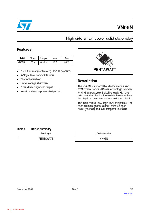
November 2008Rev 21/16VN05NHigh side smart power solid state relayFeatures■Output current (continuous): 13A @ T c =25°C ■5V logic level compatible input ■Thermal shutdown ■Under voltage shutdown ■Open drain diagnostic output ■Very low standby power dissipationDescriptionThe VN05N is a monolithic device made using STMicroelectronics VIPower technology, intended for driving resistive or inductive loads with one side grounded. Built-in thermal shutdown protects the chip from over temperature and short circuit. The input control is 5V logic level compatible. The open drain diagnostic output indicates open circuit (no load) and over temperature status.Type V DSS R DS(on)I OUT V CC VN05N60 V0.18 Ω13 A26 VTable 1.Device summaryPackage Order codes PENTAWATTVN05NContents VN05NContents1Block diagram and pin description . . . . . . . . . . . . . . . . . . . . . . . . . . . . . 52Electrical specifications . . . . . . . . . . . . . . . . . . . . . . . . . . . . . . . . . . . . . . 62.1Absolute maximum ratings . . . . . . . . . . . . . . . . . . . . . . . . . . . . . . . . . . . . . 62.2Thermal data . . . . . . . . . . . . . . . . . . . . . . . . . . . . . . . . . . . . . . . . . . . . . . . 72.3Electrical characteristics . . . . . . . . . . . . . . . . . . . . . . . . . . . . . . . . . . . . . . . 72.4Electrical characteristics curves . . . . . . . . . . . . . . . . . . . . . . . . . . . . . . . . 103Application information . . . . . . . . . . . . . . . . . . . . . . . . . . . . . . . . . . . . . 113.1Functional description . . . . . . . . . . . . . . . . . . . . . . . . . . . . . . . . . . . . . . . 123.2Protecting the device against reverse battery . . . . . . . . . . . . . . . . . . . . . 124Package and packing information . . . . . . . . . . . . . . . . . . . . . . . . . . . . . 134.1ECOP ACK® packages . . . . . . . . . . . . . . . . . . . . . . . . . . . . . . . . . . . . . . . 134.2PENTAWATT mechanical data . . . . . . . . . . . . . . . . . . . . . . . . . . . . . . . . . 13 5Revision history . . . . . . . . . . . . . . . . . . . . . . . . . . . . . . . . . . . . . . . . . . . 152/16VN05N List of tables List of tablesTable 1.Device summary. . . . . . . . . . . . . . . . . . . . . . . . . . . . . . . . . . . . . . . . . . . . . . . . . . . . . . . . . . 1 Table 2.Absolute maximum ratings. . . . . . . . . . . . . . . . . . . . . . . . . . . . . . . . . . . . . . . . . . . . . . . . . . 6 Table 3.Thermal data. . . . . . . . . . . . . . . . . . . . . . . . . . . . . . . . . . . . . . . . . . . . . . . . . . . . . . . . . . . . . 7 Table 4.Power . . . . . . . . . . . . . . . . . . . . . . . . . . . . . . . . . . . . . . . . . . . . . . . . . . . . . . . . . . . . . . . . . . 7 Table 5.Switching (V CC=13V) . . . . . . . . . . . . . . . . . . . . . . . . . . . . . . . . . . . . . . . . . . . . . . . . . . . . . . 7 Table 6.Logic inputs. . . . . . . . . . . . . . . . . . . . . . . . . . . . . . . . . . . . . . . . . . . . . . . . . . . . . . . . . . . . . . 8 Table 7.Protections and diagnostics . . . . . . . . . . . . . . . . . . . . . . . . . . . . . . . . . . . . . . . . . . . . . . . . . 8 Table 8.Truth table. . . . . . . . . . . . . . . . . . . . . . . . . . . . . . . . . . . . . . . . . . . . . . . . . . . . . . . . . . . . . . . 8 Table 9.PENTAWATT mechanical data . . . . . . . . . . . . . . . . . . . . . . . . . . . . . . . . . . . . . . . . . . . . . 14 Table 10.Document revision history . . . . . . . . . . . . . . . . . . . . . . . . . . . . . . . . . . . . . . . . . . . . . . . . . 153/16List of figures VN05N List of figuresFigure 1.Block diagram. . . . . . . . . . . . . . . . . . . . . . . . . . . . . . . . . . . . . . . . . . . . . . . . . . . . . . . . . . . . 5 Figure 2.Configuration diagram (top view) . . . . . . . . . . . . . . . . . . . . . . . . . . . . . . . . . . . . . . . . . . . . . 5 Figure 3.Current and voltage conventions . . . . . . . . . . . . . . . . . . . . . . . . . . . . . . . . . . . . . . . . . . . . . 6 Figure 4.Waveforms . . . . . . . . . . . . . . . . . . . . . . . . . . . . . . . . . . . . . . . . . . . . . . . . . . . . . . . . . . . . . . 9 Figure 5.Over current test circuit. . . . . . . . . . . . . . . . . . . . . . . . . . . . . . . . . . . . . . . . . . . . . . . . . . . . . 9 Figure 6.R DS(on) vs junction temperature . . . . . . . . . . . . . . . . . . . . . . . . . . . . . . . . . . . . . . . . . . . . 10 Figure 7.R DS(on) vs supply voltage . . . . . . . . . . . . . . . . . . . . . . . . . . . . . . . . . . . . . . . . . . . . . . . . . 10 Figure 8.R DS(on) vs output current. . . . . . . . . . . . . . . . . . . . . . . . . . . . . . . . . . . . . . . . . . . . . . . . . . 10 Figure 9.Input voltages vs junction temperature. . . . . . . . . . . . . . . . . . . . . . . . . . . . . . . . . . . . . . . . 10 Figure 10.Output current derating. . . . . . . . . . . . . . . . . . . . . . . . . . . . . . . . . . . . . . . . . . . . . . . . . . . . 10 Figure 11.Open load vs junction temperature. . . . . . . . . . . . . . . . . . . . . . . . . . . . . . . . . . . . . . . . . . . 10 Figure 12.Typical application circuit with a schottky diode for reverse supply protection. . . . . . . . . . 11 Figure 13.Typical application circuit with separate signal ground. . . . . . . . . . . . . . . . . . . . . . . . . . . . 11 Figure 14.PENTAWATT package dimensions . . . . . . . . . . . . . . . . . . . . . . . . . . . . . . . . . . . . . . . . . . 13 4/16VN05N Block diagram and pin description5/161 Block diagram and pin descriptionFigure 1.Block diagramFigure 2.Configuration diagram (top view)PENTAWATT6/162 Electrical specificationsFigure 3.Current and voltage conventions2.1 Absolute maximum ratingsStressing the device above the rating listed in the “Absolute maximum ratings” table maycause permanent damage to the device. These are stress ratings only and operation of the device at these or any other conditions above those indicated in the operating sections of this specification is not implied. Exposure to Absolute maximum rating conditions for extended periods may affect device reliability. Refer also to the STMicroelectronics sure program and other relevant quality document.INPUTI SI INV INV CCSTATUSI ST ATV STA TGNDV CCI OUTV OUTI GNDOUTPUTV FTable 2.Absolute maximum ratingsSymbolParameterValue Unit V(BR)DSS Drain-Source breakdown voltage 60V IOUT Output current (cont.)13A IRReverse output current-13A IIN Input current±10mA -V CC Reverse supply voltage -4V IST A T Status current ±10mA VESD Electrostatic discharge (1.5 k Ω, 100 pF) 2000V Ptot Power dissipation at T c ≤ 25 °C 56W Tj Junction operating temperature -40 to 150 °C TstgStorage temperature-55 to 150°C7/162.2 Thermal data2.3 Electrical characteristicsValues specified in this section are for V CC = 13V; -40°C<T j <125°C, unless otherwise stated.Table 3.Thermal dataSymbol ParameterMax. valueUnit R thj-case Thermal resistance junction-case 2.2°C/W R thj-ambThermal resistance junction-ambient60°C/WTable 4.PowerSymbol ParameterTest conditionsMin.Typ.Max.Unit V CC Supply voltage 726V Ron On state resistance I OUT = 6 AI OUT = 6 A Tj = 25°C 0.360.18ΩΩI SSupply currentOff state Tj ≥ 25 °C On state5015µA mATable 5.Switching (V CC =13V)Symbol ParameterTest conditionsMin.Typ.Max.Unitt d(on)Turn-on delay time of output current I OUT = 6 A resistive load Input rise time < 0.1 ms Tj=25 °C 15µs t r Rise time of output currentI OUT = 6 A resistive loadInput rise time < 0.1 ms Tj=25 °C30µs t d(off)Turn-off delay time of output current I OUT = 6 A Resistive load Input rise time < 0.1 ms Tj=25 °C 20µs t fFall time of output currentI OUT = 6 A resistive loadInput rise time < 0.1 ms Tj=25 °C 10µs dV OUT /dt (on)Turn-on current slope I OUT = 6 A I OUT = IOV 0.52A/µs A/µs dV OUT /dt (off)Turn-off current slopeI OUT = 6 A I OUT = IOV24A/µs A/µs8/16Table 6.Logic inputsSymbol ParameterTest conditionsMin.Typ.Max.Unit V IL Input low level voltage 0.8V V IH (1)1.The V IH is internally clamped at 6V about. It is possible to connect this pin to an higher voltage via an external resistorcalculated to not exceed 10 mA at the input pin.Input high level voltage 2V V I(hyst.)Input hysteresis voltage 0.5V I IN Input current V IN = 5 V 250500µA V ICLInput clamp voltageI IN = 10 mA I IN = -10 mA6-0.7V VTable 7.Protections and diagnosticsSymbol ParameterTest conditions Min.Typ.Max.Unit V STAT (1)1.Status determination > 100 µs after the switching edge.Status voltage output low I STAT = 1.6 mA0.4V V USD Under voltage shutdown 6.5V V SCL (1)Status clamp voltage I STA T = 10 mA I STA T = -10 mA 6-0.7V V t SCSwitch-off time in short circuit condition at start-up R LOAD < 10 m Ω Tc= 25 °C1.55msI OV Over current R LOAD < 10 m Ω -40 ≤ Tc ≤ 125 °C 60A I AV Average current in short circuit R LOAD < 10 m Ω Tc= 85 °C1.4A I OL Open load current level5180mA T TSD Thermal shutdown temperature 140°C T RReset temperature125°CTable 8.Truth tableConditions Input Output DiagnosticNormal operation L H L H H H Open circuit (no load)H H L Over-temperature H L L Under-voltageXLHFigure 4.WaveformsFigure 5.Over current test circuit9/1610/162.4 Electrical characteristics curvesFigure 6.R DS(on) vs junctiontemperatureFigure 7.R DS(on) vs supply voltageFigure 8.R DS(on)vs output current Figure 9.Input voltages vs junctiontemperatureFigure 10.Output current deratingFigure 11.Open load vs junctiontemperature分销商库存信息:STMVN05N-E VN05N。
irf540nspbf中文资料
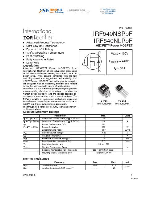
IRF540NSPbF IRF540NLPbFHEXFET ® Power MOSFET3/18/04 1Advanced HEXFET ® Power MOSFETs from International Rectifier utilize advanced processing techniques to achieve extremely low on-resistance per silicon area. This benefit, combined with the fast switching speed and ruggedized device design that HEXFET power MOSFETs are well known for, provides the designer with an extremely efficient and reliable device for use in a wide variety of applications.The D 2Pak is a surface mount power package capable of accommodating die sizes up to HEX-4. It provides the highest power capability and the lowest possible on-resistance in any existing surface mount package. The D 2Pak is suitable for high current applications because of its low internal connection resistance and can dissipate up to 2.0W in a typical surface mount application.The through-hole version (IRF540NL) is available for low-profile applications.lAdvanced Process Technology l Ultra Low On-Resistance l Dynamic dv/dt Ratingl 175°C Operating Temperature l Fast Switchingl Fully Avalanche Rated l Lead-Free DescriptionAbsolute Maximum RatingsParameterMax.UnitsI D @ T C= 25°C Continuous Drain Current, V GS @ 10V 33I D @ T C = 100°C Continuous Drain Current, V GS @ 10V 23A I DMPulsed Drain Current 110P D @T C = 25°C Power Dissipation 130W Linear Derating Factor 0.87W/°C V GS Gate-to-Source Voltage ± 20V I AR Avalanche Current16A E AR Repetitive Avalanche Energy 13mJ dv/dt Peak Diode Recovery dv/dt 7.0V/ns T J Operating Junction and-55 to + 175T STGStorage Temperature RangeSoldering Temperature, for 10 seconds 300 (1.6mm from case )°CMounting torque, 6-32 or M3 srew10 lbf•in (1.1N•m)D 2Pak IRF540NSPbF TO-262IRF540NLPbFParameterTyp.Max.UnitsR θJC Junction-to-Case––– 1.15R θJAJunction-to-Ambient (PCB mount)**–––40Thermal Resistance°C/WPD - 95130IRF540NS/LPbFSource-Drain Ratings and CharacteristicsRepetitive rating; pulse width limited bymax. junction temperature. (See fig. 11) Starting T J = 25°C, L =1.5mHR G = 25Ω, I AS = 16A. (See Figure 12)I SD ≤ 16A , di/d t ≤ 340A/µs, V DD ≤ V (BR)DSS , T J ≤ 175°CPulse width ≤ 400µs; duty cycle ≤ 2%.Notes:This is a typical value at device destruction and represents operation outside rated limits.This is a calculated value limited to T J = 175°C . Uses IRF540N data and test conditions.**When mounted on 1" square PCB (FR-4 or G-10 Material). For recommended footprint and soldering techniques refer to application note #AN-994Electrical Characteristics @ T J = 25°C (unless otherwise specified)IRF540NS/LPbF 3Fig 4. Normalized On-ResistanceVs. TemperatureIRF540NS/LPbFFig 8. Maximum Safe Operating AreaGate-to-Source VoltageDrain-to-Source Voltage Fig 7. Typical Source-Drain DiodeForward Voltage1101001000V DS , Drain-toSource Voltage (V)0.11101001000I D , D r a i n -t o -S o u r c e C u r r e n t (A )IRF540NS/LPbF 5Fig 11. Maximum Effective Transient Thermal Impedance, Junction-to-CaseCase TemperatureV V d(on)rd(off)fV DDFig 10a. Switching Time Test CircuitFig 10b. Switching Time WaveformsIRF540NS/LPbF6VDSCurrent Sampling ResistorsV GSFig 13b. Gate Charge Test CircuitFig 13a. Basic Gate Charge Waveform Fig 12b. Unclamped Inductive WaveformsI ASFig 12c. Maximum Avalanche EnergyVs. Drain CurrentV DDIRF540NS/LPbF 7Peak Diode Recovery dv/dt Test CircuitV DD* Reverse Polarity of D.U.T for P-ChannelV GS*** V GS = 5.0V for Logic Level and 3V Drive Devices Fig 14. For N-channel HEXFET ® power MOSFETsTO-262 Package OutlineIRF540NS/LPbFData and specifications subject to change without notice.This product has been designed and qualified for the industrial market.Qualification Standards can be found on IR’s Web site.IR WORLD HEADQUARTERS: 233 Kansas St., El Segundo, California 90245, USA Tel: (310) 252-7105TAC Fax: (310) 252-7903Visit us at for sales contact information .03/04344TRRFEED DIRECTION1.85 (.073)1.65 (.065)1.60 (.063)1.50 (.059)4.10 (.161)3.90 (.153)TRLFEED DIRECTION 10.90 (.429)10.70 (.421)16.10 (.634)15.90 (.626)1.75 (.069)1.25 (.049)11.60 (.457)11.40 (.449)15.42 (.609)15.22 (.601)4.72 (.136)4.52 (.178)24.30 (.957)23.90 (.941)0.368 (.0145)0.342 (.0135)1.60 (.063)1.50 (.059)13.50 (.532)12.80 (.504)330.00(14.173) MAX.27.40 (1.079)23.90 (.941)60.00 (2.362) MIN.30.40 (1.197) MAX.26.40 (1.039)24.40 (.961)NOTES :1. COMFORMS TO EIA-418.2. CONTROLLING DIMENSION: MILLIMETER.3. DIMENSION MEASURED @ HUB.4. INCLUDES FLANGE DISTORTION @ OUTER EDGE.D 2Pak Tape & Reel InfomationDimensions are shown in millimeters (inches)/package/。
F40UP20DN中文资料

FFAF40UP20DN Ultrafast Recovery Power RectifierFFAF40UP20DN Ultrafast Recovery Power RectifierFFAF40UP20DN Ultrafast Recovery Power RectifierTRADEMARKSThe following are registered and unregistered trademarks Fairchild Semiconductor owns or is authorized to use and is not intended to be an exhaustive list of all such trademarks.DISCLAIMERFAIRCHILD SEMICONDUCTOR RESERVES THE RIGHT TO MAKE CHANGES WITHOUT FURTHER NOTICE TO ANY PRODUCTS HEREIN TO IMPROVE RELIABILITY, FUNCTION OR DESIGN. FAIRCHILD DOES NOT ASSUME ANY LIABILITY ARISING OUT OF THE APPLICATION OR USE OF ANY PRODUCT OR CIRCUIT DESCRIBED HEREIN; NEITHER DOES IT CONVEY ANY LICENSE UNDER ITS PATENT RIGHTS, NOR THE RIGHTS OF OTHERS.LIFE SUPPORT POLICYFAIRCHILD’S PRODUCTS ARE NOT AUTHORIZED FOR USE AS CRITICAL COMPONENTS IN LIFE SUPPORT DEVICES OR SYSTEMS WITHOUT THE EXPRESS WRITTEN APPROVAL OF FAIRCHILD SEMICONDUCTOR CORPORATION.As used herein:1. Life support devices or systems are devices or systems which,(a) are intended for surgical implant into the body, or (b) support or sustain life, or (c) whose failure to perform when properly used in accordance with instructions for use provided in the labeling,can be reasonably expected to result in significant injury to the user.2. A critical component is any component of a life support device or system whose failure to perform can be reasonably expected to cause the failure of the life support device or system, or to affect its safety or effectiveness.PRODUCT STATUS DEFINITIONS Definition of TermsDatasheet Identification Product Status DefinitionAdvance InformationFormative or In Design This datasheet contains the design specifications for product development. Specifications may change in any manner without notice.PreliminaryFirst ProductionThis datasheet contains preliminary data, andsupplementary data will be published at a later date.Fairchild Semiconductor reserves the right to make changes at any time without notice in order to improve design.No Identification Needed Full ProductionThis datasheet contains final specifications. Fairchild Semiconductor reserves the right to make changes at any time without notice in order to improve design.Obsolete Not In ProductionThis datasheet contains specifications on a product that has been discontinued by Fairchild semiconductor.The datasheet is printed for reference information only.FAST ®FASTr™FPS™FRFET™GlobalOptoisolator™GTO™HiSeC™I 2C™i-Lo ™ImpliedDisconnect™IntelliMAX™ISOPLANAR™LittleFET™MICROCOUPLER™MicroFET™MicroPak™MICROWIRE™MSX™MSXPro™OCX™OCXPro™OPTOLOGIC ®OPTOPLANAR™PACMAN™POP™Power247™PowerEdge™PowerSaver™PowerTrench ®QFET ®QS™QT Optoelectronics™Quiet Series™RapidConfigure™RapidConnect™µSerDes™Scalar Pump™SILENT SWITCHER ®SMART START™SPM™Stealth™SuperFET™SuperSOT™-3SuperSOT™-6SuperSOT™-8SyncFET™TCM™TinyLogic ®TINYOPTO™TruTranslation™UHC™UltraFET ®UniFET™VCX™Wire™A CEx™ActiveArray™Bottomless™Build it Now™CoolFET™CROSSVOLT ™DOME™EcoSPARK™E 2CMOS™EnSigna™FACT™FACT Quiet Series™Across the board. Around the world.™The Power Franchise ®Programmable Active Droop™Rev. I18。
QS5K2TR;中文规格书,Datasheet资料
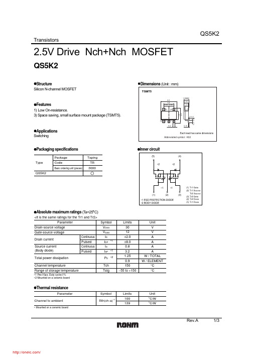
TransistorsRev.A 1/32.5V Drive Nch+Nch MOSFETQS5K2z Structure z Dimensions (Unit : mm) Silicon N-channel MOSFETz Features1) Low On-resistance.3) Space saving, small surface mount package (TSMT5).zSwitchingz Packaging specifications z Inner circuitz Absolute maximum ratings (T a=25°C)∗1∗2∗1ParameterV V DSS Symbol V V GSS A I DA I DP A I SAI SP W / TOTAL P D °C Tch °CTstgLimits Unit Drain-source voltage Gate-source voltage Drain current Total power dissipation Channel temperatureRange of storage temperatureContinuous Pulsed Continuous Pulsed∗1 Pw ≤10µs, Duty cycle ≤1%∗2 Mounted on a ceramic boardSource current (Body diode)30150−55 to +15012±2.0±8.00.83.21.25W / ELEMENT0.9<It is the same ratings for the Tr1 and Tr2>z Thermal resistanceParameter°C/W Rth(ch-a)Symbol Limits Unit Channel to ambient100°C/W139∗ Mounted on a ceramic board∗TransistorsRev.A 2/3z Electrical characteristics (T a=25°C)z Body diode characteristics (Source-drain) (T a=25°C)V SD −−1.2VI S = 3.2A, V GS =0VForward voltage∗ PulsedParameter Symbol Min.Typ.Max.UnitConditions∗<It is the same characteristics for the Tr1 and Tr2>TransistorsRev.A 3/3DRAIN-SOURCE VOLTAGE : V DS (V)101001000C A P A C I T A N C E : C (p F )Fig.1 Typical Capacitancevs. Drain-Source VoltageGATE-SOURCE VOLTAGE : V GS (V)0.0010.010.1110D R A I N C U R RE N T : I D (A )Fig.4 Typical Transfer CharacteristicsSOURCE-DRAIN VOLTAGE : V SD(V)S O U R C E C U R R E N T : I S (A )Fig.6 Source Current vs. Source-Drain VoltageGATE-SOURCE VOLTAGE : V GS (V)100200300S T A T I C D R A I N -S O U R C E O N -S T A T E R E S I S TA N C E : R D S (m Ω)Fig.5 Static Drain-SourceOn-State Resistance vs.Gate source Voltagez Electrical characteristics curvesDRAIN CURRENT : I D (A)1101001000S W I T C H I N G T I M E : t (n s )Fig.2 Switching CharacteristicsTOTAL GATE CHARGE : Qg (nC)123456G A T E -S O U R C E V O L T A G E : V G S (V )Fig.3 Dynamic Input CharacteristicsDRAIN CURRENT : I D (A)S T A T I C D R A I N -S O U R C E O N -S T A T E R E S I S T A N C E : R D S (o n ) (m Ω)Fig.7 Static Drain-Source On-State Resistance vs. Drain Current ( Ι )DRAIN CURRENT : I D (A)S T A T I C D R A I N -S O U R C E O N -S T A T E R E S I S T A N C E : R D S (o n ) (m Ω)Fig.8 Static Drain-Source On-State Resistance vs. Drain Current ( ΙΙ )DRAIN CURRENT : I D (A)S T A T I C D R A I N -S O U R C E O N -S T A T E R E S I S T A N C E : R D S (o n ) (m Ω)Fig.9 Static Drain-Source On-State Resistance vs. Drain Current ( ΙΙΙ )AppendixAbout Export Control Order in JapanProducts described herein are the objects of controlled goods in Annex 1 (Item 16) of Export T rade ControlOrder in Japan.In case of export from Japan, please confirm if it applies to "objective" criteria or an "informed" (by MITI clause)on the basis of "catch all controls for Non-Proliferation of Weapons of Mass Destruction.Appendix1-Rev1.1分销商库存信息: ROHMQS5K2TR。
NS4225用户手册V1.0

N S4225用户手册V1.0深圳市纳芯威科技有限公司2014年08月修改历史日期版本作者修改说明目录1功能说明 (5)2主要特性 (5)3应用领域 (5)4典型应用电路 (5)5极限参数 (6)6电气特性 (7)7芯片管脚描述 (8)7.1 NS4225管脚分配图 (8)7.2 NS4225引脚功能描述 (8)8NS4225典型参考特性 (9)9NS4225应用说明 (10)9.1 芯片基本结构描述 (10)9.2 低功耗关断控制端/SD (11)9.3 并联BTL输出设置端PBTL (11)9.4 NS4225应用图示 (12)9.4.1 差分输入BTL输出立体声模式 (12)9.4.2 单端输入BTL输出立体声模式 (12)9.4.3 差分输入PBTL输出单声道模式 (13)9.4.4 单端输入PBTL输出单声道模式 (13)9.5 NS4225应用参数设置 (14)9.5.1 放大器增益设置 (14)9.5.2 输入电容Ci的选取 (14)9.5.3 电源去耦电容 (15)9.6 输出滤波器 (15)9.7 layout建议 (16)9.8 测试电路 (16)10芯片的封装 (17)图目录图1 NS4225典型应用电路 (6)图2 NS4225管脚分配图(top view) (8)图3 NS4225原理框图 (10)图4 /SD管脚设置 (11)图5 PBTL管脚设置 (11)图6 差分输入BTL输出立体声模式 (12)图7 单端输入BTL输出立体声模式 (12)图8 差分输入PBTL输出单声道模式 (13)图9 单端输入PBTL输出单声道模式 (13)图10 输入高通网络 (14)图11 输入高通滤波器曲线 (14)图12 输出端加磁珠应用图 (15)图13 负载为8Ω,转折频率为27kHz的LC输出滤波器 (15)图14 负载为4Ω,转折频率为27kHz的LC输出滤波器 (16)图15 NS4225测试电路 (16)图16 TSSOP-24封装尺寸图 (17)表目录表1 芯片最大物理极限值 (6)表2 NS4225电气特性 (7)表3 NS4225管脚描述 (8)1功能说明NS4225是一款无需滤波器,每声道可输出25W的D类立体声音频功率放大器。
RFP50N05资料

RFG50N05, RFP50N05 50 50 50 120 ±20 132 0.88
Refer to UIS SOA Curve -55 to 175
300 260
UNITS V V A A V W
W/ oC
oC
oC oC
CAUTION: Stresses above those listed in “Absolute Maximum Ratings” may cause permanent damage to the device. This is a stress only rating and operation of the device at these or any other conditions above those indicated in the operational sections of this specification is not implied.
IDSS
IGSS rDS(ON)
t(ON) td(ON)
tr
VDS = Rated BVDSS, VGS = 0V VDS = 0.8 x Rated BVDSS, VGS = 0V, TJ = 150oC
VGS = ±20V
ID = 50A, VGS = 10V (Figure 7)
VDD = 25V, ID ≈ 25A, RL = 1.0Ω, RGS = 6.67Ω, VGS = 10V (Figure 11)
or 407-727-9207 | Copyright © Intersil Corporation 1999
元器件交易网
RFG50N05, RFP50N05
Absolute Maximum Ratings TC = 25oC, Unless Otherwise Specified
- 1、下载文档前请自行甄别文档内容的完整性,平台不提供额外的编辑、内容补充、找答案等附加服务。
- 2、"仅部分预览"的文档,不可在线预览部分如存在完整性等问题,可反馈申请退款(可完整预览的文档不适用该条件!)。
- 3、如文档侵犯您的权益,请联系客服反馈,我们会尽快为您处理(人工客服工作时间:9:00-18:30)。
NSR05F40NXT5GSchottky Barrier DiodeThese Schottky barrier diodes are optimized for low forward voltage drop and low leakage current and are offered in a Chip Scale Package (CSP) to reduce board space. The low thermal resistance enables designers to meet the challenging task of achieving higher efficiency and meeting reduced space requirements.Features•Low Forward V oltage Drop − 420 mV @ 500 mA•Low Reverse Current − 15 m A @ 10 V VR•500 mA of Continuous Forward Current•ESD Rating − Human Body Model: Class 3B− Machine Model: Class C•High Switching Speed•These Devices are Pb−Free, Halogen Free/BFR Free and are RoHS CompliantTypical Applications•LCD and Keypad Backlighting•Camera Photo Flash•Buck and Boost dc−dc Converters•Reverse V oltage and Current Protection•Clamping and ProtectionMarkets•Mobile Handsets•MP3 Players•Digital Camera and Camcorders•Notebook PCs & PDAs•GPSMAXIMUM RATINGSRating Symbol Value Unit Reverse Voltage V R40V Forward Current (DC)I F500mAForward Surge Current(60 Hz @ 1 cycle)I FSM10ARepetitive Peak Forward Current(Pulse Wave = 1 sec, Duty Cycle = 66%)I FRM 4.0AESD Rating:Human Body ModelMachine Model ESD> 8> 400kVVStresses exceeding Maximum Ratings may damage the device. MaximumRatings are stress ratings only. Functional operation above the Recommended Operating Conditions is not implied. Extended exposure to stresses above the Recommended Operating Conditions may affect device reliability.40 V SCHOTTKYBARRIER DIODE12Device Package Shipping†ORDERING INFORMATIONNSR05F40NXT5G DSN2(Pb−Free)5000 / Tape & Reel†For information on tape and reel specifications, including part orientation and tape sizes, please refer to our Tape and Reel Packaging Specifications Brochure, BRD8011/D.DSN2(0402)CASE 152ACMARKINGDIAGRAM05F40= Specific Device CodeYYY= Year CodeTHERMAL CHARACTERISTICSCharacteristic Symbol Min Typ Max UnitThermal ResistanceJunction−to−Ambient (Note 1)Total Power Dissipation @ T A = 25°C R q JAP D240521°C/WmWThermal ResistanceJunction−to−Ambient (Note 2)Total Power Dissipation @ T A = 25°C R q JAP D941.3°C/WWStorage Temperature Range T stg−40 to +125°C Junction Temperature T J+150°C1.Mounted onto a 4 in square FR−4 board 50 mm sq. 1 oz. Cu 0.06” thick single sided. Operating to steady state.2.Mounted onto a 4 in square FR−4 board 1 in sq. 1 oz. Cu 0.06” thick single sided. Operating to steady state.ELECTRICAL CHARACTERISTICS (T A = 25°C unless otherwise noted)Characteristic Symbol Min Typ Max UnitReverse Leakage (V R = 10 V)(V R = 40 V)I R1575m AForward Voltage(I F = 100 mA)(I F = 500 mA)V F0.3400.4200.3600.460VTYPICAL CHARACTERISTICSFigure 1. Forward VoltageFigure 2. Leakage CurrentV F , FORWARD VOLTAGE (V)V R , REVERSE VOLTAGE (V)I F , F O R W A R D C U R R E N T (A )I r , R E V E R S E C U R R E N T (m A )Figure 3. Total CapacitanceV R , REVERSE VOLTAGE (V)C T , T O T A L C A P A C I T A N C E (p F )PACKAGE DIMENSIONSDSN2, 1.0x0.6, 0.575P , (0402)CASE 152AC −01ISSUE BYEAR CODEDEVICE CODE (EXAMPLE)CATHODE BAND MONTHCODINGNOTES:1.DIMENSIONING AND TOLERANCING PER ASME Y14.5M, 1994.2.CONTROLLING DIMENSION: MILLIMETERS.BOTTOM VIEWDIM MIN MAX MILLIMETERS A 0.250.31A1−−−0.05b 0.450.55D 1.00 BSC E 0.60 BSC L 0.850.95SOLDER FOOTPRINT*DIMENSIONS: MILLIMETERS*For additional information on our Pb −Free strategy and soldering details, please download the ON Semiconductor Soldering and Mounting Techniques Reference Manual, SOLDERRM/D.See Application Note AND8398/D for more mounting details L20.350.45L30.200.30RECOMMENDED ON Semiconductor and are registered trademarks of Semiconductor Components Industries, LLC (SCILLC). SCILLC reserves the right to make changes without further notice to any products herein. SCILLC makes no warranty, representation or guarantee regarding the suitability of its products for any particular purpose, nor does SCILLC assume any liability arising out of the application or use of any product or circuit, and specifically disclaims any and all liability, including without limitation special, consequential or incidental damages.“Typical” parameters which may be provided in SCILLC data sheets and/or specifications can and do vary in different applications and actual performance may vary over time. All operating parameters, including “Typicals” must be validated for each customer application by customer’s technical experts. SCILLC does not convey any license under its patent rights nor the rights of others. SCILLC products are not designed, intended, or authorized for use as components in systems intended for surgical implant into the body, or other applications intended to support or sustain life, or for any other application in which the failure of the SCILLC product could create a situation where personal injury or death may occur. Should Buyer purchase or use SCILLC products for any such unintended or unauthorized application, Buyer shall indemnify and hold SCILLC and its officers, employees, subsidiaries, affiliates,and distributors harmless against all claims, costs, damages, and expenses, and reasonable attorney fees arising out of, directly or indirectly, any claim of personal injury or death associated with such unintended or unauthorized use, even if such claim alleges that SCILLC was negligent regarding the design or manufacture of the part. SCILLC is an Equal Opportunity/Affirmative Action Employer. This literature is subject to all applicable copyright laws and is not for resale in any manner.PUBLICATION ORDERING INFORMATION分销商库存信息: ONSEMINSR05F40NXT5G。