RT9198-49GY中文资料
ERA-4SM中文资料(mini circuits)中文数据手册「EasyDatasheet - 矽搜」

14.4 14.2 13.0 12.0 11.3 .003 .0025 .0031 .0042 .0051 35 30 21 21 35 21 21 16 23 17.5 17.3 16.1 14 11.7 17.8 16.5
36.1 35 30.4 25 4 4.2 4.2 4.5 80 65 4.6 -2.9 10.4 196
4
GHz
15
dB
13.6
12.2
.006
dB/°C
.006
.006
.008
.01
dB
dB
dB dBm
dBm dBm
5
dB
5.2
5.2
5.5
psec
mA
4.9
V
mV/°C
mV/mA
°C/W
绝对最大额定值
参数
额定值
工作温度 储存温度 工作电流 功耗 输入功率
-45°C至85°C -65℃至150℃
85mA 417mW 20 dBm的
RF IN
RF-OUT and DC-IN
GROUND
RF-OUT and DC-IN 3
4 GND
GND 2
1 RF IN
功能
RF在
引脚数
1
RF-OUT和DC-IN
3
GND
2,4
描述
射频输入引脚.该引脚需要使用选择用于操作频率外部隔直流电容器.
RF输出和偏置引脚.直流电压出现在该引脚;因此一个DC阻断 电容器是必要正确操作. RF扼流圈需要喂DC偏置 无RF信号损失,由于偏置连接,如图中"推荐 应用电路". 连接到地面.通孔使用,如图中"建议布局PCB 设计",以减少为最佳性能接地路径电感.
RFC4K中文资料

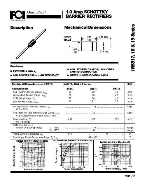
DO-41
1.0(25.4) MIN. .205(5.2) .166(4.2)
.034(0.9) .028(0.7)
DIA. DIA.
MECHANICAL DATA
·Case: Molded plastic ·Epoxy: UL94V-0 rate flame retardant ·Lead: MIL-STD- 202E, Method 208 guaranteed ·Polarity:Color band denotes cathode end ·Mounting position: Any ·Weight: 0.35 grams
元器件交易网
CHONG PINGYANG ELECTRONICS CO.,LTD.
RFC2K THRU RFC4K
HIGH VOLTAGE FAST RECOVERY RECTIFIER
VOLTAGE:2000-3000V CURRENT:0.2A
FEATURES
·fast switching ·Low leakage ·high current capability ·high surge capability ·High reliability
.107(2.7) .080(2.0) 1.0(25.4) MIN.
Dimensions in inches and (millimeters)
MAXIMUM RATINGS AND ELECTRONICAL CHARACTERISTICS
Ratings at 25℃ ambient temperature unless otherwise specified. Single phase, half wave, 60Hz,resistive or inductive load. For capacitive load, derate current by 20%. SYMBOL Maximum Recurrent Peak Reverse Voltage Maximum RMS Voltage Maximum DC Blocking Voltage Maximum Average Forward rectified Current at TA=50°C Peak Forward Surge Current 8.3ms single half sine-wave superimposed on rate load (JEDEC method) Maximum Forward Voltage Drop per element at 0.2A DC Maximum DC Reverse Current @ TA=25°C at Rated DC Blocking Voltage @ TA=100°C Maximum Full Load Reverse Current Average, Full Cycle .375”(9.5mm) lead length at TL=75°C Typical Junction Capacitance (Note) Maximum Reverse Recovery Time (Note) Notes: VRRM VRMS VDC Io RFC2K 2000 1400 2000 RFC3K 3000 2100 3000 0.2 RFC4K 4000 2800 4000
in5819中文资料_数据手册_参数
TJ = 75oC TJ = 25oC
1N5819
Reverse Voltage (Volts)
Forward Voltage (Volts)
Reverse Voltage (VR) - Volts Page 7-3
采购电子元器件上万联芯城,只售原装现货,万联芯城专 为终端客户提供电子元器件配单业务,货源均来自原厂及 代理商,客户只需访问官网,联系在线客服提交 BOM 表, 即可获得报价,为客户节省采购成本,满足客户物料需求, 点击进入万联芯城。
IN5817 20 20 20 14
IN5818 30 30 30 21
IN5819
40
Volts
40
Volts
40
Volts
28
Volts
Average Forward Rectified Current...IF(av) @ TA = 55°C
............................................. 1.0 ............................................... Amps
Typical Junction Capacitance...CJ
110
< ...................... .70 .................... > pF
Operating & Storage Temperature Range...TJ, TSTRG
....................................... -65 to 125 ............................................ °C
P8TG-4818E41中文资料

Available Inputs:
24 and 48 VDC Wide Input 4:1
Available Outputs:
3.3, 5, 12, 15 and 18 VDC
Other specifications please enquire.
Electrical Specifications
(Typical at + 25° C, nominal input voltage, rated output current unless otherwise specified) Input Specifications Voltage range Filter Isolation Specifications Rated voltage Leakage current Resistance Capacitance Output Specifications Voltage accuracy Ripple and noise (at 20 MHz BW) Short circuit protection Line voltage regulation Load voltage regulation Temperature coefficient General Specifications Efficiency Switching frequency Environmental Specifications Operating temperature (ambient) Storage temperature Derating Humidity Cooling Physical Characteristics Dimensions Weight Case material 9 - 36 VDC (24 VDC), 18 - 72 VDC (48 VDC) Pi Network 1500 Vdc 1 mA 109 Ohm 80 pF typ. +/- 1 % typ. +/-2% max. 60 mV p-p, max. Continuous , restart automatic +/- 0,5 % max. +/- 0,5 % max. +/- 0,02 % / °C 70 % to 85 % 250 KHz, typ. -40°C to +85°C - 55 °C to + 125 °C See graph Up to 90 %, non condensing Free air convection 31,75 x 20,32 x 10,16 mm 1,25 x 0,80 x 0,40 inches 18,5 g Non conductive black plastic
1N4749中文资料

Fig 1. Thermal resistance from junction to tie-point as a function of pulse duration; lead length 4 mm
7. Characteristics
Table 7. Characteristics Tj = 25 °C unless otherwise specified.
[1] The series consists of 22 types with nominal working voltages from 3.3 V to 24 V.
Version SOD66
Table 4. Marking codes Type number 1N4728A to 1N4749A
The series consists of 22 types with nominal working voltages from 3.3 to 24 V.
1.2 Features
I Total power dissipation: max. ≤ 1000 mW
I Working voltage range: nom. 3.3 V to 24 V
3 of 10
NXP Semiconductors
1N4728A to 1N4749A
Voltage regulator diodes
Table 8. Characteristics per type Tj = 25 °C unless otherwise specified.
Type number
146
1
10
4
133
0.5
10
5
121
0.5
AO4918中文资料

Symbol V DS I FM T J , T STGMaximum SchottkyUnits30V T A =25°CParameterReverse VoltageA2.2203T A =70°C Pulsed Diode Forward Current BContinuous Forward Current AP D I F T A =25°C T A =70°CJunction and Storage Temperature RangePower Dissipation AW 1.28-55 to 150°C2AO4918AO4918Symbol Units R θJL Symbol Units R θJLR θJLTHIS PRODUCT HAS BEEN DESIGNED AND QUALIFIED FOR THE CONSUMER MARKET. APPLICATIONS OR USES AS CRITICAL COMPONENTS IN LIFE SUPPORT DEVICES OR SYSTEMS ARE NOT AUTHORIZED. AOS DOES NOT ASSUME ANY LIABILITY ARISING OUT OF SUCH APPLICATIONS OR USES OF ITS PRODUCTS. AOS RESERVES THE RIGHT TO IMPROVE PRODUCT DESIGN,FUNCTIONS AND RELIABILITY WITHOUT NOTICE.Maximum Junction-to-Lead CSteady-State8626.650.4R θJA 62.5Maximum Junction-to-AmbientAt ≤ 10s R θJA Maximum Junction-to-Ambient ASteady-State 110110Maximum Junction-to-Lead CSteady-State 30.5Typ Maximum Junction-to-AmbientASteady-State Parameter: Thermal Characteristics MOSFET Q1Maximum Junction-to-AmbientAt ≤ 10s 40Thermal Characteristics Schottky62.5405381.962.5°C/WMaximum Junction-to-AmbientASteady-State Max °C/W°C/WParameter: Thermal Characteristics MOSFET Q2Typ Max Maximum Junction-to-AmbientAt ≤ 10s R θJA 5381.9110Maximum Junction-to-Lead CSteady-State 30.540A: The value of R θJA is measured with the device mounted on 1in 2 FR-4 board with 2oz. Copper, in a still air environment with T A =25°C. The value in any given application depends on the user's specific board design. The current rating is based on the t ≤ 10s thermal resistance rating.B: Repetitive rating, pulse width limited by junction temperature.C. The R θJA is the sum of the thermal impedence from junction to lead R θJL and lead to ambient.D. The static characteristics in Figures 1 to 6 are obtained using 80 µs pulses, duty cycle 0.5% max.E. These tests are performed with the device mounted on 1 in 2 FR-4 board with 2oz. Copper, in a still air environment with T A =25°C. The SOA curve provides a single pulse rating.F. The Schottky appears in parallel with the MOSFET body diode, even though it is a separate chip. Therefore, we provide the net forward drop, capacitance and recovery characteristics of the MOSFET and Schottky. However, the thermal resistance is specified for each chip separately. Rev4: August 2005AO4918SymbolMin TypMax UnitsBV DSS 30V0.0070.053.2101220I GSS 100nA V GS(th)0.6 1.12V I D(ON)40A 11.714.5T J =125°C15.41913.116m Ωg FS 3037S V SD 0.460.5V I S3.5A C iss 37404488pF C oss 295pF C rss 186pF R g0.86 1.1ΩQ g 30.537nC Q gs 4.5nC Q gd 8.5nC t D(on)69ns t r 8.212ns t D(off)54.575ns t f 10.515ns t rr Body Diode + Schottky Reverse Recovery Time I F =9.3A, dI/dt=100A/µs 23.528ns Q rrBody Diode + Schottky Reverse Recovery ChargeI F =9.3A, dI/dt=100A/µs13.316nCTHIS PRODUCT HAS BEEN DESIGNED AND QUALIFIED FOR THE CONSUMER MARKET. APPLICATIONS OR USES AS CRITICAL COMPONENTS IN LIFE SUPPORT DEVICES OR SYSTEMS ARE NOT AUTHORIZED. AOS DOES NOT ASSUME ANY LIABILITY ARISING OUT OF SUCH APPLICATIONS OR USES OF ITS PRODUCTS. AOS RESERVES THE RIGHT TO IMPROVE PRODUCT DESIGN,FUNCTIONS AND RELIABILITY WITHOUT NOTICE.Gate Source Charge Gate Drain Charge Turn-On DelayTime V GS =10V, V DS =15V, R L =1.6Ω, R GEN =3ΩV GS =4.5V, V DS =15V, I D =9.3ATurn-On Rise Time Turn-Off DelayTime Turn-Off Fall TimeSWITCHING PARAMETERS Total Gate Charge Gate resistanceV GS =0V, V DS =0V, f=1MHzForward TransconductanceV DS =5V, I D =9.3ADiode+Schottky Forward Voltage I S =1A Maximum Body-Diode+Schottky Continuous CurrentDYNAMIC PARAMETERS Input Capacitance V GS =0V, V DS =15V, f=1MHz Output Capacitance (FET + Schottky)Reverse Transfer Capacitance R DS(ON)Static Drain-Source On-ResistanceV GS =10V, I D =9.3Am ΩV GS =4.5V, I D =8.8AGate Threshold Voltage V DS =V GS I D =250µA On state drain currentV GS =4.5V, V DS =5V mA Gate-Body leakage current V DS =0V, V GS = ±12V V R =30V, T J =125°C V R =30V, T J =150°C Drain-Source Breakdown Voltage I D =250µA, V GS =0V I DSS Zero Gate Voltage Drain Current.(Set by Schottky leakage)V R =30VQ1 Electrical Characteristics (T J =25°C unless otherwise noted)ParameterConditions STATIC PARAMETERS A: The value of R θJA is measured with the device mounted on 1in 2 FR-4 board with 2oz. Copper, in a still air environment with T A =25°C. The value in any given application depends on the user's specific board design. The current rating is based on the t ≤ 10s thermal resistance rating.B: Repetitive rating, pulse width limited by junction temperature.C. The R θJA is the sum of the thermal impedence from junction to lead R θJL and lead to ambient.D. The static characteristics in Figures 1 to 6,12,14 are obtained using 80 µs pulses, duty cycle 0.5% max.E. These tests are performed with the device mounted on 1 in 2 FR-4 board with 2oz. Copper, in a still air environment with T A =25°C. The SOA curve provides a single pulse rating.F. The Schottky appears in parallel with the MOSFET body diode, even though it is a separate chip. Therefore, we provide the net forward drop, capacitance and recovery characteristics of the MOSFET and Schottky. However, the thermal resistance is specified for each chip separately Rev4: August 2005.AO4918Q1 TYPICAL ELECTRICAL AND THERMAL CHARACTERISTICSAO4918AO4918SymbolMin TypMax UnitsBV DSS 30V 0.0041T J =55°C5I GSS 100nA V GS(th)1 1.83V I D(ON)30A 14.918T J =125°C222721.627m Ωg FS 23S V SD 0.450.5V I S3A C iss 10401250pF C oss 180pF C rss 110pF R g0.70.85ΩQ g (10V)19.224nC Q g 9.3612nC Q gs 2.6nC Q gd 4.2nC t D(on) 5.27.5ns t r 4.4 6.5ns t D(off)17.325ns t f 3.35ns t rr Body Diode Reverse Recovery TimeI F =8.5A, dI/dt=100A/µs16.721ns Q rrBody Diode Reverse Recovery Charge I F =8.5A, dI/dt=100A/µs6.710nCTHIS PRODUCT HAS BEEN DESIGNED AND QUALIFIED FOR THE CONSUMER MARKET. APPLICATIONS OR USES AS CRITICAL COMPONENTS IN LIFE SUPPORT DEVICES OR SYSTEMS ARE NOT AUTHORIZED. AOS DOES NOT ASSUME ANY LIABILITY ARISIN OUT OF SUCH APPLICATIONS OR USES OF ITS PRODUCTS. AOS RESERVES THE RIGHT TO IMPROVE PRODUCT DESIGN,FUNCTIONS AND RELIABILITY WITHOUT NOTICE.V GS =10V, V DS =15V, I D =8.3ATotal Gate Charge Turn-On Rise Time Turn-Off DelayTime Turn-Off Fall TimeReverse Transfer Capacitance SWITCHING PARAMETERS Total Gate Charge Gate Source Charge Gate Drain Charge Turn-On DelayTime V GS =10V, V DS =15V, R L =1.8Ω, R GEN =3ΩGate resistanceV GS =0V, V DS =0V, f=1MHzForward TransconductanceV DS =5V, I D =8.3ADiode+Schottky Forward Voltage I S =1AMaximum Body-Diode+Schottky Continuous CurrentDYNAMIC PARAMETERS Input Capacitance V GS =0V, V DS =15V, f=1MHz Output Capacitance R DS(ON)Static Drain-Source On-ResistanceV GS =10V, I D =8.3Am ΩV GS =4.5V, I D =7AGate Threshold Voltage V DS =V GS I D =250µA On state drain currentV GS =4.5V, V DS =5V µA Gate-Body leakage current V DS =0V, V GS = ±20V Drain-Source Breakdown Voltage I D =250µA, V GS =0V I DSS Zero Gate Voltage Drain Current V DS =24V, V GS =0VQ2 Electrical Characteristics (T J =25°C unless otherwise noted)ParameterConditions STATIC PARAMETERS A: The value of R θJA is measured with the device mounted on 1in 2 FR-4 board with 2oz. Copper, in a still air environment with T A =25°C. The value in any given application depends on the user's specific board design. The current rating is based on the t ≤ 10s thermal resistance rating.B: Repetitive rating, pulse width limited by junction temperature.C. The R θJA is the sum of the thermal impedence from junction to lead R θJL and lead to ambient.D. The static characteristics in Figures 1 to 6,12,14 are obtained using 80 µs pulses, duty cycle 0.5% max.E. These tests are performed with the device mounted on 1 in 2FR-4 board with 2oz. Copper, in a still air environment with T A =25°C. The SOA curve provides a single pulse rating. Rev4: August 2005AO4918Q2 Electrical Characteristics (T J=25°C unless otherwise noted)AO4918。
EPCS4SI8N中文资料(Altera)中文数据手册「EasyDatasheet - 矽搜」
串行配置器件
EPCS4 — — — — — — — — — —
EPCS16 v (2) v (2)
— — — — — — — —
EPCS64 EPCS128
v
v
v
v
v
v
v
v
v (2)
v
—
v
v
v
v
v
v
v
v (2)
v
表4-4 列出每个Stratix II GX FPGA和所使用串行配置器件 配置文件大小. Stratix II GX器件可以使用EPCS16,EPCS64,或 EPCS128.
处理器通过内存访问未使用闪存重新可编程内存超过10万次擦除编程写存储扇区防护护支持使用状态寄存器位在系统编程支持srunner软件驱动程序在系统编程支持usb冲击波byteblaster
芯片中文手册,看全文,戳
C51014-3.2
4.串行配置器件(EPCS1, EPCS4,EPCS16,EPCS64和EPCS128)
4–4
功能说明
表4-5 列出每个Stratix II FPGA和所使用串行配置设备 配置文件大小. Stratix II器件可与EPCS4,EPCS16,EPCS64,或使用 EPCS128.
表 4-5. 对于Stratix II器件串行配置设备支持
Stratix II器件
原始二进制文件大小
( 位 )(1)
表 4-4. 为Stratix II GX器件串行配置设备支持
Stratix II GX器件
原始二进制文件
大 小 ( 位 )(1)
EP2SGX30C
9,640,672
EP2SGX30D
EP2SGX60C
GLT4160L04-50TC中文资料

GLT4160L044M X 4 CMOS DYNAMIC RAM WITH EXTENDED DATA OUTPUTMay 2001 (Rev.3.1)G-Link TechnologyG-Link Technology Corporation,TaiwanFeatures :Description :∗ 4,194,304 words by 4 bits organization.∗ Fast access time and cycle time ∗ Low power dissipation.∗ Read-Modify-Write, RAS -Only Refresh,CAS -Before-RAS Refresh, Hidden Refresh.∗ 2,048 refresh cycles per 32ms.∗ Available in 300 mil 26(24) SOJ and TSOPII.∗ 3.3V ±0.3V Vcc Power Supply voltage .∗ All inputs and Outputs are LVTTL compatible.∗ Extended Data-Out (EDO) Page accesscycle.∗ Self-refresh Capability . (S-Version).The GLT4160L04 is a high-performance CMOS dynamic random access memory containing 16,777,216 bits organized in a x4configuration. The GLT4160L04 offers page cycle access with Extended Data Output.The GLT4160L04 has 11 row- and 11column-addresses, and accepts 2048-cycle refresh in 32 ms.The GLT4160L04 provides EDO PAGE MODE operation which allows for fast data access within a row-address defined boundary, up to 2048 x 4 bits with cycle times as short as 18ns.GLT4160L044M X 4 CMOS DYNAMIC RAM WITH EXTENDED DATA OUTPUTMay 2001 (Rev.3.1)G-Link TechnologyG-Link Technology Corporation,TaiwanPin Configuration :V cc DQ 0A 0A 1A 2A 31234568910111213222119181716151426252423A 9A 8A 7A 6OE CAS V SS DQ 3DQ 1WE RAS NC V CCDQ 2A 5A 4V SSA 10V cc DQ 0A 10A 0A 1A 2A 31234568910111213222119181716151426252423A 9A 8A 7A 6OE CAS V SS DQ3DQ 1WE RAS NC V CCDQ 2A 5A 4V SSPin Descriptions:GLT4160L04300mil 26(24) TSOPIIGLT4160L04300mil 26(24) SOJGLT4160L044M X 4 CMOS DYNAMIC RAM WITH EXTENDED DATA OUTPUTMay 2001 (Rev.3.1)G-Link TechnologyG-Link Technology Corporation,TaiwanAbsolute Maximum Ratings*Capacitance*Operating Temperature, T A (ambient).............................................….0°C to+70°C For Extended Temperature……………..-20°C to 85°CStorage Temperature(plastic)............-55°C to +150°CVoltage Relative to V SS ........................-0.5V to + 4.6V Power Dissipation...............................................1.0W*Note: Operation above Absolute Maximum Ratings canaversely affect device reliability.*Note: Capacitance is sampled and not 100% testedElectrical Specificationsl All voltages are referenced to GND.l After power up, wait more than 200µs and then, execute eight CAS -before-RASor RAS -onlyrefresh cycles as dummy cycles to initialize internal circuit.Block Diagram :A 1A 2A 3A 4A 5A 6A 7A 8A 9A WE CASDQ 0DQ 1DQ 2DQ 3OEV DD V SSA 0GLT4160L044M X 4 CMOS DYNAMIC RAM WITH EXTENDED DATA OUTPUTMay 2001 (Rev.3.1)G-Link TechnologyG-Link Technology Corporation,TaiwanTruth Table:GLT4160L044M X 4 CMOS DYNAMIC RAM WITH EXTENDED DATA OUTPUTMay 2001 (Rev.3.1)G-Link TechnologyG-Link Technology Corporation,TaiwanDC and Operating Characteristics (1-2)1. I CC is dependent on output loading when the device output is selected. Specified I CC (max.) is measured with the output open.2. I CC is dependent upon the number of address transitions specified ICC(max.) is measured with a maximum of one transition per address cyclein random Read/Write and EDO Fast Page Mode.3. Specified V IL (min.) is steady state operation. During transitions V IL (min.) may undershoot to –1V for a period not to exceed 15ns. All ACparameters are measured with V IL (min.)≥V SS and V IH (max.)≤V CC .4. Specified V IH (max.) is steady state operation . During transitions V IH (max.) may overshoot to V CC +1V for a period not to exceed 15ns. All ACparameters are measured with V IL (min.) ≥ V SS and VIH(max.) ≤ V CC . 5. S-Version.GLT4160L044M X 4 CMOS DYNAMIC RAM WITH EXTENDED DATA OUTPUTMay 2001 (Rev.3.1)G-Link TechnologyG-Link Technology Corporation,TaiwanAC CharacteristicsT A =0°C to 70°C , -20°C to 85°C V CC = 3.3 V ± 0.3V, VIH/VIL = 3/0 V, V OH /V OL = 2/0.8VGLT4160L044M X 4 CMOS DYNAMIC RAM WITH EXTENDED DATA OUTPUTMay 2001 (Rev.3.1)G-Link TechnologyG-Link Technology Corporation,TaiwanAC CharacteristicsGLT4160L044M X 4 CMOS DYNAMIC RAM WITH EXTENDED DATA OUTPUTMay 2001 (Rev.3.1) ArrayG-Link Technology G-Link Technology Corporation,TaiwanGLT4160L044M X 4 CMOS DYNAMIC RAM WITH EXTENDED DATA OUTPUTMay 2001 (Rev.3.1) ArrayG-Link Technology G-Link Technology Corporation,TaiwanGLT4160L044M X 4 CMOS DYNAMIC RAM WITH EXTENDED DATA OUTPUTMay 2001 (Rev.3.1)G-Link TechnologyG-Link Technology Corporation,TaiwanNotes:1. Measure with a load equivalent to one TTL input and 100 pF.2. Assumes that t RCD ≤ t RCD (max.). If t RCD is greater than t RCD (max.), access time will be t AA dominant.3. Assumes that t RAD ≤ t RAD (max.). If t RAD is greater than t RCD (max.), access time will be controlled by t CAC .4. Either t RRH or t RCH must be satisfied for a Read Cycle.5. Access time is determined by the longest of t AA , t CAC and t CPA .6. Assumes that t RAD ≥ t RAD (max.).7. Operation within the t RAD (max.) limit ensures that t RAC (max.) can be met. t RAD (max.) is specified as a reference point only. If t RAD is greater than the specified t RAD (max.) limit, the access time is controlled by t CAA and t CAC .8. t WCS , t RWD , t AWD and t CWD are not restrictive operating parameters. 9. t WCS (min.) must be satisfied in an Early Write Cycle.10. t DS and t DH are referenced to the latter occurrence of CAS or WE .11. t T is measured between V IH (min.) and V IL (max.). AC-measurements assume t T = 2 ns.GLT4160L044M X 4 CMOS DYNAMIC RAM WITH EXTENDED DATA OUTPUTMay 2001 (Rev.3.1)G-Link TechnologyG-Link Technology Corporation,TaiwanRead CYCLEROW ADDRESSCOLUMN ADDRESSDATA-OUTt RC t RASt RPt CRPt CSHt RCDt RSH t CASt CRPt ASRt RAHt RAD t ASCt CAHt RAL t RCH t RRHt ARt RCSt AAt OEAt CEZt OEZt CACt CLZt RACDon't CareV IH-V IL-V IH-V IL-CASV IH-V IL-AddressV IH-V IL-WEV IH-V IL-OEV OH-V OL-DQEarly Write Cycle NOTE : D OUT = OPENV IH-V IL-RASV V CASV V AddressV V WEV V V IH-V IL-DQDon't CareGLT4160L044M X 4 CMOS DYNAMIC RAM WITH EXTENDED DATA OUTPUTMay 2001 (Rev.3.1)G-Link TechnologyG-Link Technology Corporation,TaiwanOE Controlled Write Cycle NOTE : D OUT = OPENDATA - INV V IL-RASV V CASV V AddressV IH-V IL-WEV IH-V IL-OEV IH-V IL-DQDon't Caret RSHV V IL-RASV V CASV V AddressV V WEV V OEV V DQDon't Caret RASt CLZAAGLT4160L044M X 4 CMOS DYNAMIC RAM WITH EXTENDED DATA OUTPUTMay 2001 (Rev.3.1)G-Link TechnologyG-Link Technology Corporation,TaiwanEDO Page Mode Read Cycle NOTE : D OUT = OPENt OLZ t RAC t CAC t OEZDATA-OUT DATA-OUTV IH-V IL-RASV V CASV IH-V IL-AddressV IH-V IL-WEV V OEDQV V Don't Caret RHCPGLT4160L044M X 4 CMOS DYNAMIC RAM WITH EXTENDED DATA OUTPUTMay 2001 (Rev.3.1)G-Link TechnologyG-Link Technology Corporation,TaiwanEDO Page Mode Read - Modify - Write Cycle NOTE : D OUT = OPENt RPV IH-VIL-RASV VCASDon't CareGLT4160L044M X 4 CMOS DYNAMIC RAM WITH EXTENDED DATA OUTPUTMay 2001 (Rev.3.1)G-Link TechnologyG-Link Technology Corporation,TaiwanCAS - Before - RAS Refresh CycleV IH-V IL-RASV IH-V IL-CASV IH-V IL-WERAS -Only Refresh CycleV IH-V IL-RASt RASt RASV IH-V IL-CASt CRPt ASRt ASR AddressV IH-V IL-Hidden Refresh Cycle ( Read )V IH-V IL-RASV V UCAS,LCASV V AddressV V WEV V OEDQV V Don't CareGLT4160L044M X 4 CMOS DYNAMIC RAM WITH EXTENDED DATA OUTPUTMay 2001 (Rev.3.1)G-Link TechnologyG-Link Technology Corporation,TaiwanHidden Refresh Cycle ( Write ) NOTE : D OUT = OPENV IH-V IL-RASV V CASV V AddressV V WEV V DQV V Don't CareGLT4160L044M X 4 CMOS DYNAMIC RAM WITH EXTENDED DATA OUTPUTMay 2001 (Rev.3.1)G-Link TechnologyG-Link Technology Corporation,TaiwanCAS-Before RAS Refresh Counter Test CycleV V V IH-V IL-Don't CareDATA-INDATA-OUT V IH-V IL-Address V V WE V V V V DQ V V WE V V V V DQ V V V V OE V V DQGLT4160L044M X 4 CMOS DYNAMIC RAM WITH EXTENDED DATA OUTPUTMay 2001 (Rev.3.1)G-Link TechnologyG-Link Technology Corporation,TaiwanTEST MODE IN CYCLEDon't CareV IH-V IL-V IH-V IL-V IH-V IL-V I/OH-V I/OL-RASCASWEDQ Test ModeBy using the test mode, the test time can be reduced. The reason for this is that, the memory emulates the x 16-bit organization during test mode. Don’t care about the input levels of the CAS input A0, A1 .(1) Setting the modeExecuting the test mode cycle (WE , CAS before RAS refresh cycle ) sets the test mode.(2) Write / read operationWhen either a “0” or a “1” is written to the input pin in test mode, this data is written to 16 bits of memory cell.Next, when the data is read from the output pin at the same address, the cell be checked.Output = “1” Normal write (all memory cells)Output = “0” Abnormal write(3) RefreshRefresh in the test mode must be performed with the RAS / CAS cycle or with the WE, CAS before RAS refresh cycle. The WE, CAS before RAS refresh cycle use the same counter as the CAS before RAS refresh’s internal counter.(4) Mode CancellationThe test mode is cancelled by executing one cycle of RAS only refresh cycle or CAS before RAS refresh cycle.GLT4160L044M X 4 CMOS DYNAMIC RAM WITH EXTENDED DATA OUTPUTMay 2001 (Rev.3.1)G-Link TechnologyG-Link Technology Corporation,TaiwanCAS-BEFORE-RAS SELF REFRESH CYCLEDon't CareV IH-V IL-V IH-V IL-V I/OH-V I/OL-CASDQV IH-V IL-WENOTE : OE , Address = Don’t CareGLT4160L044M X 4 CMOS DYNAMIC RAM WITH EXTENDED DATA OUTPUTMay 2001 (Rev.3.1)G-Link TechnologyG-Link Technology Corporation,TaiwanOrdering InformationPart NumberSPEEDPOWERFEATURETEMPERATUREPACKAGEGLT4160L04-40J340ns Normal EDO Commercial SOJ 300mil 26(24)L GLT4160L04-50J350ns Normal EDO Commercial SOJ 300mil 26(24)L GLT4160L04-60J360ns Normal EDO Commercial SOJ 300mil 26(24)L GLT4160L04-70J370ns Normal EDO Commercial SOJ 300mil 26(24)L GLT4160L04E-40J340ns Normal EDO Extended SOJ 300mil 26(24)L GLT4160L04E-50J350ns Normal EDO Extended SOJ 300mil 26(24)L GLT4160L04E-60J360ns Normal EDO Extended SOJ 300mil 26(24)L GLT4160L04E-70J370ns Normal EDO Extended SOJ 300mil 26(24)L GLT4160L04S-40J340ns Self Refresh EDO Commercial SOJ 300mil 26(24)L GLT4160L04S-50J350ns Self Refresh EDO Commercial SOJ 300mil 26(24)L GLT4160L04S-60J360ns Self Refresh EDO Commercial SOJ 300mil 26(24)L GLT4160L04S-70J370ns Self Refresh EDO Commercial SOJ 300mil 26(24)L GLT4160L04SE-40J340ns Self Refresh EDO Extended SOJ 300mil 26(24)L GLT4160L04SE-50J350ns Self Refresh EDO Extended SOJ 300mil 26(24)L GLT4160L04SE-60J360ns Self Refresh EDO Extended SOJ 300mil 26(24)L GLT4160L04SE-70J370ns Self Refresh EDO Extended SOJ 300mil 26(24)L GLT4160L04-40TC 40ns Normal EDO Commercial TSOPII 300mil 26(24)L GLT4160L04-50TC 50ns Normal EDO Commercial TSOPII 300mil 26(24)L GLT4160L04-60TC 60ns Normal EDO Commercial TSOPII 300mil 26(24)L GLT4160L04-70TC 70ns Normal EDO Commercial TSOPII 300mil 26(24)L GLT4160L04E-40TC 40ns Normal EDO Extended TSOPII 300mil 26(24)L GLT4160L04E-50TC 50ns Normal EDO Extended TSOPII 300mil 26(24)L GLT4160L04E-60TC 60ns Normal EDO Extended TSOPII 300mil 26(24)L GLT4160L04E-70TC 70ns Normal EDO Extended TSOPII 300mil 26(24)L GLT4160L04S-40TC 40ns Self Refresh EDO Commercial TSOPII 300mil 26(24)L GLT4160L04S-50TC 50ns Self Refresh EDO Commercial TSOPII 300mil 26(24)L GLT4160L04S-60TC 60ns Self Refresh EDO Commercial TSOPII 300mil 26(24)L GLT4160L04S-70TC 70ns Self Refresh EDO Commercial TSOPII 300mil 26(24)L GLT4160L04SE-40TC 40ns Self Refresh EDO Extended TSOPII 300mil 26(24)L GLT4160L04SE-50TC 50ns Self Refresh EDO Extended TSOPII 300mil 26(24)L GLT4160L04SE-60TC 60ns Self Refresh EDO Extended TSOPII 300mil 26(24)L GLT4160L04SE-70TC70nsSelf RefreshEDOExtendedTSOPII 300mil 26(24)LGLT4160L044M X 4 CMOS DYNAMIC RAM WITH EXTENDED DATA OUTPUTMay 2001 (Rev.3.1) ArrayG-Link Technology G-Link Technology Corporation,TaiwanGLT4160L044M X 4 CMOS DYNAMIC RAM WITH EXTENDED DATA OUTPUTMay 2001 (Rev.3.1)G-Link TechnologyG-Link Technology Corporation,TaiwanPackage Information300mil 24/26 Lead Thin Small Outline Package (TSOP) TYPE II。