2SK2586中文资料
2SK3356资料
DATA SHEETDocument No.D14133EJ1V0DS00 (1st edition)The information in this document is subject to change without notice. Before using this document, pleaseconfirm that this is the latest version.Not all devices/types available in every country. Please check with local NEC representative for availability and additional information.The mark 5 shows major revised points.DESCRIPTIONThe 2SK3356 is N-channel MOS Field Effect Transistor designed for high current switching applications.FEATURES•Super low on-state resistance:R DS(on)1 = 8.0 m Ω MAX. (V GS = 10 V, I D = 38 A)R DS(on)2 = 12 m Ω MAX. (V GS = 4 V, I D = 38 A)•Low C iss : C iss = 6300 pF TYP.•Built-in gate protection diodeABSOLUTE MAXIMUM RATINGS (T A = 25°C)Drain to Source Voltage V DSS 60V Gate to Source Voltage V GSS(AC)±20V Drain Current (DC)I D(DC)±75A Drain Current (pulse) Note1I D(pulse)±300A Total Power Dissipation (T C = 25°C)P T 130W Total Power Dissipation (T A = 25°C)P T 3.0W Channel Temperature T ch 150°C Storage TemperatureT stg –55 to +150°C Single Avalanche Current Note2I AS 55A Single Avalanche Energy Note2E AS302mJNotes 1.PW ≤ 10 µs, Duty cycle ≤ 1 %2. Starting T ch = 25 °C, R G = 25 Ω, V GS = 20 V → 0 VTHERMAL RESISTANCEChannel to Case Rth(ch-C)0.93°C/W Channel to AmbientRth(ch-A)41.7°C/WORDERING INFORMATIONPART NUMBERPACKAGE 2SK3356TO-3P55555552ELECTRICAL CHARACTERISTICS (T A = 25 °C)CHARACTERISTICSSYMBOL TEST CONDITIONSMIN.TYP.MAX.UNIT Drain to Source On-state ResistanceR DS(on)1V GS = 10 V, I D = 38 A 6.38.0m ΩR DS(on)2V GS = 4 V, I D = 38 A 8.012m ΩGate to Source Cut-off Voltage V GS(off)V DS = 10 V, I D = 1 mA 1.5 2.0 2.5VForward Transfer Admittance | y fs|V DS = 10 V, I D = 38 A 3557SDrain Leakage CurrentI DSS V DS = 60 V, V GS = 0 V 10µA Gate to Source Leakage Current I GSS V GS = ±20 V, V DS = 0V±10µA Input Capacitance C iss V DS = 10 V, V GS = 0 V, f = 1 MHz6300pF Output CapacitanceC oss 1000pF Reverse Transfer Capacitance C rss 490pF Turn-on Delay Time t d(on)ID = 38 A, V GS(on) = 10 V, V DD = 30 V,90ns Rise Timet r R G = 10 Ω1100ns Turn-off Delay Time t d(off)300ns Fall Timet f 400ns Total Gate Charge Q G I D = 75 A , V DD = 48 V, V GS = 10 V 106nC Gate to Source Charge Q GS 20nC Gate to Drain Charge Q GD 30nC Body Diode Forward Voltage V F(S-D)I F = 75 A, V GS = 0 V 1.0V Reverse Recovery Time t rr I F = 75 A, V GS = 0 V,55ns Reverse Recovery ChargeQ rrdi/dt = 100 A/µs100nC5TEST CIRCUIT 3 GATE CHARGEV GS = 20 → 0 TEST CIRCUIT 1 AVALANCHE CAPABILITYL DDTEST CIRCUIT 2 SWITCHING TIMEL DDτ = 1 µsDuty Cycle ≤ 1 %3PACKAGE DRAWING (Unit: mm)Remark The diode connected between the gate and source of the transistor serves as a protector against ESD.When this device actually used, an additional protection circuit is externally required if a voltage exceeding the rated voltage may be applied to this device.TO-3P (MP-88)EQUIVALENT CIRCUITBody DiodeDiodeDrain• The information in this document is subject to change without notice. Before using this document, please confirm that this is the latest version.• No part of this document may be copied or reproduced in any form or by any means without the prior written consent of NEC Corporation. NEC Corporation assumes no responsibility for any errors which may appear in this document.• NEC Corporation does not assume any liability for infringement of patents, copyrights or other intellectual propertyrights of third parties by or arising from use of a device described herein or any other liability arising from useof such device. No license, either express, implied or otherwise, is granted under any patents, copyrights or otherintellectual property rights of NEC Corporation or others.• Descriptions of circuits, software, and other related information in this document are provided for illustrative purposes in semiconductor product operation and application examples. The incorporation of these circuits,software, and information in the design of the customer's equipment shall be done under the full responsibilityof the customer. NEC Corporation assumes no responsibility for any losses incurred by the customer or third parties arising from the use of these circuits, software, and information.• While NEC Corporation has been making continuous effort to enhance the reliability of its semiconductor devices,the possibility of defects cannot be eliminated entirely. To minimize risks of damage or injury to persons orproperty arising from a defect in an NEC semiconductor device, customers must incorporate sufficient safety measures in its design, such as redundancy, fire-containment, and anti-failure features.• NEC devices are classified into the following three quality grades:"Standard", "Special", and "Specific". The Specific quality grade applies only to devices developed based on acustomer designated "quality assurance program" for a specific application. The recommended applications ofa device depend on its quality grade, as indicated below. Customers must check the quality grade of each devicebefore using it in a particular application.Standard: Computers, office equipment, communications equipment, test and measurement equipment,audio and visual equipment, home electronic appliances, machine tools, personal electronic equipment and industrial robotsSpecial: Transportation equipment (automobiles, trains, ships, etc.), traffic control systems, anti-disastersystems, anti-crime systems, safety equipment and medical equipment (not specifically designed for life support)Specific: Aircraft, aerospace equipment, submersible repeaters, nuclear reactor control systems, lifesupport systems or medical equipment for life support, etc.The quality grade of NEC devices is "Standard" unless otherwise specified in NEC's Data Sheets or Data Books. If customers intend to use NEC devices for applications other than those specified for Standard quality grade, they should contact an NEC sales representative in advance.M7 98. 8。
2586规格书 译文
EUP25862012年2月DS2586 Ver1.01小包装,高性能,Asynchronies提升WLED司机描述这是一个EUP2586高频,异步的推动转换器设计用于驱动白光LED阵列。
与集成开关电源和2 0.19限流,EUP2586提供足够的驱动性能7 ~ 10英寸液晶背光(13串3个或者4个发光二极管每个)。
该装置采用电流模式、固定频率建筑规范LED电流,这是通过一个外部电流感测电阻。
它的低200毫伏电压降低功率损耗和反馈提高效率。
内置过压保护功能(OVP),西南销监视输出电压如果一个关闭装置过电压情况包括软启动、过电流限制,热保护和低电压闭锁。
这EUP2586是可得到的在小TSOT23-5包裹送到客户提供最佳的解决方案对印刷电路板的空间储蓄和总BOM成本。
特征2.6 V输入范围5.5 V内部0.19,18 V MOSFET开关效率高达到93%在表面温度低ILED = 180麻1兆赫开关频率2一个限流导致过电压保护开放内部Soft-StartPWM(脉宽调制)和直流模糊控制可在TSOT23-5包装RoHS认证,并无100%的铅无卤应用中部背光Netbook背光便携式媒体播放器GPS导航系统典型应用电路图1。
申请EUP2586 PWM变白光LED驱动EUP25862012年2月DS2586 Ver1.02框图图2。
框图销配置包装类型销配置TSOT23-5销描述销TSOT23-5描述1 SW开关的密码。
这是流失的内部电源开关。
连接电感/二极管在这里。
减少微量区这个别针减少电磁干扰(EMI)。
3弗拉维奥-布里亚托利反馈的密码。
参考电压是200毫伏。
连接阴极发光二极管(LED)和最低的电阻在这里。
根据计算电阻价值公式:= 200千瓦/ ILED RFB4在芯片使别针。
连接到1.4 V或更高的电压,使装置,0.3 V或更少电压禁用设备。
5在输入电压。
EUP25862012年2月DS2586 Ver1.03订购信息订单号码包装类型标识操作温度范围内EUP2586OIR1 TSOT23-5xxxxxAd00-40°C + 85°C□□□□EUP2586□□□□□□□□□□□□无铅代码包装记者:磁带和卷操作温度范围内我:行业标准包装类型服务员:TSOTEUP25862012年2月DS2586 Ver1.04绝对最大额定值(1)在,嗯,弗拉维奥-布里亚托利对地- - - - - - - - - - - - - - - - - - - - - - - - - - - - - - - - - - - - - - - - - - - - - - - - - - - - - - - - - - - - - - - - - - - - - - - - - - - - - - - - - - - - - - - - -0.3 V 6 V对地的SW - - - - - - - - - - - - - - - - - - - - - - - - - - - - - - - - - - - - - - - - - - - - - - - - - - - - - - - - - - - - - - - - - - - - - - - - - - - - - - - - - - - - - - - - - - - - - - - - -0.3 V至18 V功耗,PD = 25°C @助教TSOT23-5 - - - - - - - - - - - - - - - - - - - - - - - - - - - - - - - - - - - - - - - - - - - - - - - - - - - - - - - - - - - - - - - - - - - - - - - - - - - - - - - - - - - - - - - - - - - - - - - - - 0.5 W包装热阻TSOT23-5,θJA - - - - - - - - - - - - - - - - - - - - - - - - - - - - - - - - - - - - - - - - - - - - - - - - - - - - - - - - - - - - - - - - - - - - - - - - - - - - - - - - - - - - - - - - - - - 200°C / W铅温度(焊接,10秒。
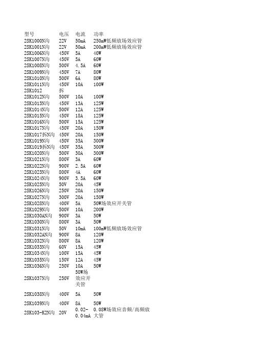
2SK系列场管参数
1mA 大管
10mA 80mW通用型场效应管
10A 100W
15A 120W
20A 130W
10mA 200mW
5A
150W
5A
150W
10mA 200mW
20A 150W
20A 150W
15A 150W
0.5- 0.25W场效应音频/高频放
1.5mA 大管
1-3mA
0.25W场效应音频/高频放 大管
拆N沟 600V 6A
600V 6A
45W
1000V 4A
100W
30V 10mA 1000V 8A 50V 25A 100V 40A 60V 40A 60V 45A 50V 10mA 50V 3-9mA
200mW 150W 45W 100W 100W 125W 250mW 0.25W
2SK112-RN沟
10mA 150mW低频放大场效应管
0.51.5mA
0.3W场效应音频(低频)管
1-3mA 0.3W场效应音频(低频)管
2-6mA 0.3W场效应音频(低频)管
4-12mA 0.3W场效应音频(低频)管
300mW
低频放
大场效
应管
50mA 150mW低频放大场效应管
2.75.5mA
0.25W
3A
45W
500V 15A 100W
450V 20A 147/290ns
拆N沟 50V 10mA
500V 20A 120W
800V 4A
80W
900V 3.5A 80W
2SK1173N沟 2SK1177N沟
50V 500V
2SK1178N沟 500V
2SK1179N沟 500V 2SK117-BLN沟 50V 2SK117-GRN沟 50V 2SK117N沟 50V 2SK117-ON沟 50V
场效应管参数大全2要点

TOSHIBA
500 8
80
关、开关整流
N-MOSFET,用于高速高电压开
TOSHIBA
500 8
40
关、开关整流
N-MOSFET,用于高速高电压开
TOSHIBA
600 6
80
关、开关整流
N-MOSFET,用于高速高电压开
TOSHIBA 关、DC-DC 转换、继电器驱动和 600 6
40
电动机驱动
N-MOSFET,用于高速高电压开
SANYO
N-MOSFET,通用开关应用
250 16
50
N-MOSFET,用于高速开关、高频
PANASONIC
250 2
30
功率放大
N-MOSFET,用于高频功率放大、
PANASONIC
15 0.05 0.2
模拟开关
NEC
N-MOSFET,用于高速开关
50 0.1 0.25
N-MOSFET,用于高速高电压开
电源、DC-DC 转换、一般功率放 500 15 125
大
N-MOSFET,用于开关
600 9
50
N-MOSFET,用于开关整流、UPS
2SK2599 2SK259H 2SK2601 2SK2602 2SK2603 2SK2604 2SK2605 2SK2606 2SK2607
型号 2SK2608 2SK260H 2SK261 2SK2610
2SK2611
NEC TOSHIBA TOSHIBA
TOSHIBA
TOSHIBA
TOSHIBA
N-MOSFET,用于开关整流、UPS
电源、DC-DC 转换、一般功率放 450 10
2SK2486中文资料
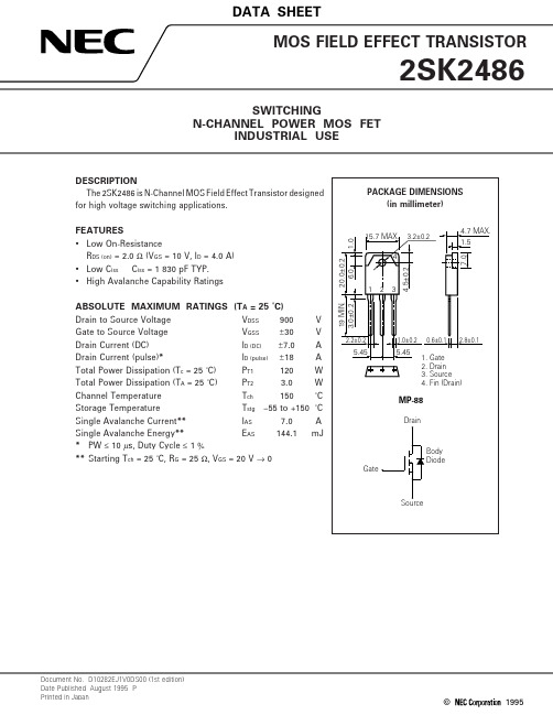
Document No. D10282EJ1V0DS00 (1st edition)Date Published August 1995 PPrinted in Japan©19952SK24862ELECTRICAL CHARACTERISTICS (T A = 25 ˚C)The application circuits and their parameters are for references only and are not intended for use in actual design-in's.Test Circuit 3 Gate ChargeV GS PGTest Circuit 1 Avalanche CapabilityLTest Circuit 2 Switching TimePG.L DDt = 1 usDuty Cycle ≤ 1 %2SK24863TYPICAL CHARACTERISTICS (T A = 25 ˚C)FORWARD BIAS SAFE OPERATING AREA V DS - Drain to Source Voltage - V I D - D r a i n C u r r e n t - ADRAIN CURRENT vs.DRAIN TO SOURCE VOLTAGEV DS - Drain to Source Voltage - VI D - D r a i n C u r r e n t - AFORWARD TRANSFER CHARACTERISTICS V GS - Gate to Source Voltage - VI D - D r a i n C u r r e n t - A0.1DERATING FACTOR OF FORWARD BIAS SAFE OPERATING AREAT C - Case Temperature - ˚C d T - P e r c e n t a g e o f R a t e d P o w e r - %TOTAL POWER DISSIPATION vs.CASE TEMPERATURET C - Case Temperature - ˚C P T - T o t a lPo w er D i s s i p a t i o n - W200204060801001201401602040608010040608010012014016014012010080604020111010051.010100102SK24864TRANSIENT THERMAL RESISTANCE vs. PULSE WIDTHPW - Pulse Width - sr t h (t ) - T r a n s i e n t T h e r m a l R e s i s t a n c e - ˚C /WFORWARD TRANSFER ADMITTANCE vs.DRAIN CURRENTI D - Drain Current - A| y f s | - F o r w a r d T r a n s f e r A d m i t t a n c e - S DRAIN TO SOURCE ON-STATE RESISTANCE vs.GATE TO SOURCE VOLTAGE V GS - Gate to Source Voltage - V R D S (o n ) - D r a i n t o S o u r c e O n -S t a t e R e s i s t a n c e - ΩDRAIN TO SOURCE ON-STATE RESISTANCE vs. DRAIN CURRENTGATE TO SOURCE CUTOFF VOLTAGE vs.CHANNEL TEMPERATURET ch - Channel Temperature - ˚CV G S (o f f ) - G a t e t o S o u r c e C u t o f f V o l t a g e - VI D - Drain Current - AR D S (o n ) - D r a i n t o S o u r c e O n -S t a t e R e s i s t a n c e - Ω3100.0010.010.111001 000 1 m10 m100 m1101001 00010101001 000355V DS = 10 V I D = 1 mA–5005010015051717246 µ100 µ2SK24865DRAIN TO SOURCE ON-STATE RESISTANCE vs.CHANNEL TEMPERATURER D S (o n ) - D r ai n t o S o u r c e O n -S t a t e R e s i s t a n c e - ΩSOURCE TO DRAIN DIODE FORWARD VOLTAGEV DS - Drain to Source Voltage - VC i s s , C o s s , C r s s - C a p a c i t a n c e - p FI D - Drain Current - A101001 00010 000V G S - G a t e t o S o u r c e V o l t a g e - VREVERSE RECOVERY TIME vs.DRAIN CURRENTI D - Drain Current - At r r - R e v e r s e R e c o v e r y t i m e - n sdi/dt = 50 A/ s V GS = 0µ100.11001 0001.010100DYNAMIC INPUT/OUTPUT CHARACTERISTICSQ g - Gate Charge - nC246810121416010 0006SINGLE AVALANCHE CURRENT vs.INDUCTIVE LOADL - Inductive Load - HI A S - S i n g l e A v a l a n c h e C u r r e n t - ASINGLE AVALANCHE ENERGY DERATING FACTORStarting T ch - Starting Channel Temperature - ˚CE n e r g y D e r a t i n gF a c t o r - %1.00251010020801201605075100125150V DD = 150 V R G = 25 ΩV GS = 20 V → 0I AS 7.0 A1006040140≥REFERENCE7[MEMO]No part of this document may be copied or reproduced in any form or by any means without the prior written consent of NEC Corporation. NEC Corporation assumes no responsibility for any errors which may appear in this document.NEC Corporation does not assume any liability for infringement of patents, copyrights or other intellectual property rights of third parties by or arising from use of a device described herein or any other liability arising from use of such device. No license, either express, implied or otherwise, is granted under any patents, copyrights or other intellectual property rights of NEC Corporation or others.While NEC Corporation has been making continuous effort to enhance the reliability of its semiconductor devices, the possibility of defects cannot be eliminated entirely. To minimize risks of damage or injury to persons or property arising from a defect in an NEC semiconductor device, customer must incorporate sufficient safety measures in its design, such as redundancy, fire-containment, and anti-failure features.NEC devices are classified into the following three quality grades:“Standard“, “Special“, and “Specific“. The Specific quality grade applies only to devices developed based ona customer designated “quality assurance program“ for a specific application. The recommended applicationsof a device depend on its quality grade, as indicated below. Customers must check the quality grade of each device before using it in a particular application.Standard:Computers, office equipment, communications equipment, test and measurement equipment, audio and visual equipment, home electronic appliances, machine tools, personal electronicequipment and industrial robotsSpecial:Transportation equipment (automobiles, trains, ships, etc.), traffic control systems, anti-disaster systems, anti-crime systems, safety equipment and medical equipment (not specifically designedfor life support)Specific:Aircrafts, aerospace equipment, submersible repeaters, nuclear reactor control systems, life support systems or medical equipment for life support, etc.The quality grade of NEC devices in “Standard“ unless otherwise specified in NEC's Data Sheets or Data Books.If customers intend to use NEC devices for applications other than those specified for Standard quality grade, they should contact NEC Sales Representative in advance.Anti-radioactive design is not implemented in this product.M4 94.11 8。
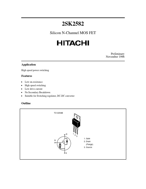
2SK2582资料
40
3
m
s
Operation in this area is 1 limited by R DS(on)
O
(1
n tio ra pe
Sh
ot
)
c (T
20
= °C 25
0.3 0.1 Ta = 25 °C 1
)
0
50
100
150 Tc (°C)
200
Case Temperature
3 10 30 100 300 1000 Drain to Source Voltage V DS (V)
2 1
Ratings 350
Unit V V A A A W
r30
13 52 13 75 150 –55 to +150
qC qC
2
元器件交易网
2SK2582
Electrical Characteristics (Ta = 25GC)
Item Drain to source breakdown voltage Gate to source breakdown voltage Gate to source leak current Symbol V(BR)DSS V(BR)GSS IGSS VGS(off) Min 350 Typ — — — — — 0.30 9.0 1250 Max — — Unit V V Test Conditions ID = 10 mA, VGS = 0 IG = r100 PA, VDS = 0 VGS = r25 V, VDS = 0 VDS =350 V, VGS = 0 ID = 1 mA, VDS = 10 V ID = 7 A 1 VGS = 10 V* ID = 7 A 1 VDS = 10 V* VDS = 10 V VGS = 0 f = 1 MHz
2SD2568中文资料(rohm)中文数据手册「EasyDatasheet - 矽搜」
0.5 (A)
1
0.5 (A)
1
0.02 BASE SATURATION VOLTAGE : V 0.01 0.001 0.002 0.005 0.01 0.02 0.05 0.1 0.2 COLLECTOR CURRENT : I
C
0.5 (A)
1
COLLECTOR CURRENT : I
图4 DC电流增益 - 集电极电流(
1/2
芯片中文手册,看全文,戳
2SD2568
晶体管电气特Biblioteka 曲线200 (mA) 160
C
Ta=25 C
mA 3.0m A 2.5m A 2.0m A 1.5m A
1 (A)
C
V CE =3V
FE
1000 500 200 100
Ta=25 C
0.5 0.2 0.1 0.05
25°C
FE
2SD2568 CPT3 PQ TL 2500
电气特性
Parameter Collector-base breakdown voltage Collector-emitter breakdown voltage Emitter-base breakdown voltage Collector cutoff current Emitter cutoff current Collector-emitter saturation voltage Base-emitter saturation voltage DC current transfer ratio Transition frequency Output capacitance
(V) 2
BE(sat)
200 100 50 20
2SC2655中文资料(secos)中文数据手册「EasyDatasheet - 矽搜」

Min. Typ. Max.
50
-
-
50
-
-
5
-
-
-
-
1
-
-
1
70
-
240
40
-
-
-
-
0.5
-
-
1.2
-
100
-
-
30
-
-
0.15
-
-
2
-
-
0.15
-
单元 V V V μA μA
V V MHz pF
μs
测试条件
IC=100μA, I E=0 IC=10mA, I B=0 IE=100μA, I C=0 VCB=50V, I E=0 VEB=5V, I C=0 VCE=2V, I C=0.5A VCE=2V, I C=1.5A IC=1A, I B=0.05A IC=1A, I B=0.05A VCE=2V, I C=0.5A VCB=10V, I E=0, f=1MHz VCC=30V IB1= -I B2=0.05A IC=1A
芯片中文手册,看全文,戳
2SC2655
2A , 50V NPN塑料封装晶体管
符合RoHS产品 "-C"后缀指定卤素及无铅
特征
低饱和电压:V 高速切换时间:T已 为补充2SA1020
CE(sat) =0.5V(Max)(I C=1A) stg=1μs(Typ.)
^ h分类
产品秩 范围
FE (1) 2SC2655-O
70-140
2SC2655-Y 120-240
收藏家
基地
发射器
TO-92MOD
A
- 1、下载文档前请自行甄别文档内容的完整性,平台不提供额外的编辑、内容补充、找答案等附加服务。
- 2、"仅部分预览"的文档,不可在线预览部分如存在完整性等问题,可反馈申请退款(可完整预览的文档不适用该条件!)。
- 3、如文档侵犯您的权益,请联系客服反馈,我们会尽快为您处理(人工客服工作时间:9:00-18:30)。
2SK2586Silicon N-Channel MOS FETADE-208-358 C4th. EditionApplicationHigh speed power switchingFeatures• Low on-resistance• R DS(on) = 7 m typ.• High speed switching• 4 V gate drive device can be driven from 5 V sourceOutline2SK25862Absolute Maximum Ratings (Ta = 25°C)ItemSymbol Ratings Unit Drain to source voltage V DSS 60V Gate to source voltage V GSS ±20V Drain current I D *260A Drain peak currentI D(pulse)*1240A Body to drain diode reverse drain current I DR *260A Avalanche current I AP *345A Avalanche energy E AR *3174mJ Channel dissipation Pch*2125W Channel temperature Tch 150°C Storage temperatureTstg–55 to +150°CNotes: 1.PW ≤ 10 µs, duty cycle ≤ 1 %2.Value at Tc = 25°C3.Value at Tch = 25°C, Rg ≥ 50 Ω2SK25863Electrical Characteristics (Ta = 25°C)ItemSymbol Min Typ Max Unit Test Conditions Drain to source breakdown voltageV (BR)DSS 60——V I D = 10 mA, V GS = 0Gate to source breakdown voltageV (BR)GSS ±20——V I G = ±100 µA, V DS = 0Gate to source leak current I GSS ——±10µA V GS = ±16 V, V DS = 0Zero gate voltage drain current I DSS——100µA V DS = 60 V, V GS = 0Gate to source cutoff voltage V GS(off) 1.0— 2.0V I D = 1 mA, V DS = 10 V Static drain to source on state resistanceR DS(on)—710m ΩI D = 30 A V GS = 10 V*1—1016m ΩI D = 30 A V GS = 4 V*1Forward transfer admittance |y fs |3560—S I D = 30 A V DS = 10 V*1Input capacitance Ciss —3550—pF V DS = 10 V Output capacitanceCoss —1760—pF V GS = 0Reverse transfer capacitance Crss —500—pF f = 1 MHz Turn-on delay time t d(on)—35—ns I D = 30 A Rise timet r —260—ns V GS = 10 V Turn-off delay time t d(off)—480—ns R L = 1.0 ΩFall timet f —370—ns Body to drain diode forward voltageV DF —0.94—V I F = 60 A, V GS = 0Body to drain diode reverse recovery time t rr—140—nsI F = 60 A, V GS = 0diF / dt = 50 A / µs Note:1.Pulse TestSee characteristic curves of 2SK2529.2SK25864Hitachi CodeJEDECEIAJWeight (reference value)TO-3P—Conforms5.0 gUnit: mmCautions1.Hitachi neither warrants nor grants licenses of any rights of Hitachi’s or any third party’s patent,copyright, trademark, or other intellectual property rights for information contained in this document.Hitachi bears no responsibility for problems that may arise with third party’s rights, includingintellectual property rights, in connection with use of the information contained in this document.2.Products and product specifications may be subject to change without notice. Confirm that you have received the latest product standards or specifications before final design, purchase or use.3.Hitachi makes every attempt to ensure that its products are of high quality and reliability. However,contact Hitachi’s sales office before using the product in an application that demands especially high quality and reliability or where its failure or malfunction may directly threaten human life or cause risk of bodily injury, such as aerospace, aeronautics, nuclear power, combustion control, transportation,traffic, safety equipment or medical equipment for life support.4.Design your application so that the product is used within the ranges guaranteed by Hitachi particularly for maximum rating, operating supply voltage range, heat radiation characteristics, installationconditions and other characteristics. Hitachi bears no responsibility for failure or damage when used beyond the guaranteed ranges. Even within the guaranteed ranges, consider normally foreseeable failure rates or failure modes in semiconductor devices and employ systemic measures such as fail-safes, so that the equipment incorporating Hitachi product does not cause bodily injury, fire or other consequential damage due to operation of the Hitachi product.5.This product is not designed to be radiation resistant.6.No one is permitted to reproduce or duplicate, in any form, the whole or part of this document without written approval from Hitachi.7.Contact Hitachi’s sales office for any questions regarding this document or Hitachi semiconductor products.Hitachi, Ltd.Semiconductor & Integrated Circuits.Nippon Bldg., 2-6-2, Ohte-machi, Chiyoda-ku, Tokyo 100-0004, Japan Tel: Tokyo (03) 3270-2111 Fax: (03) 3270-5109Copyright ' Hitachi, Ltd., 1999. All rights reserved. Printed in Japan.Hitachi Asia Pte. Ltd.16 Collyer Quay #20-00Hitachi TowerSingapore 049318Tel: 535-2100Fax: 535-1533URLNorthAmerica : http:/Europe : /hel/ecg Asia (Singapore): .sg/grp3/sicd/index.htm Asia (Taiwan): /E/Product/SICD_Frame.htm Asia (HongKong): /eng/bo/grp3/index.htm Japan : http://www.hitachi.co.jp/Sicd/indx.htmHitachi Asia Ltd.Taipei Branch Office3F, Hung Kuo Building. No.167, Tun-Hwa North Road, Taipei (105)Tel: <886> (2) 2718-3666Fax: <886> (2) 2718-8180Hitachi Asia (Hong Kong) Ltd.Group III (Electronic Components)7/F., North Tower, World Finance Centre,Harbour City, Canton Road, Tsim Sha Tsui,Kowloon, Hong Kong Tel: <852> (2) 735 9218Fax: <852> (2) 730 0281 Telex: 40815 HITEC HXHitachi Europe Ltd.Electronic Components Group.Whitebrook ParkLower Cookham Road MaidenheadBerkshire SL6 8YA, United Kingdom Tel: <44> (1628) 585000Fax: <44> (1628) 778322Hitachi Europe GmbHElectronic components Group Dornacher Stra§e 3D-85622 Feldkirchen, Munich GermanyTel: <49> (89) 9 9180-0Fax: <49> (89) 9 29 30 00Hitachi Semiconductor (America) Inc.179 East Tasman Drive,San Jose,CA 95134 Tel: <1> (408) 433-1990Fax: <1>(408) 433-0223For further information write to:。