MAX16013中文资料
MAX1132-MAX1133

MAX1132/MAX1133
Ordering Information
PART MAX1132ACAP* TEMP. RANGE 0°C to +70°C 0°C to +70°C PIN-PACKAGE 20 SSOP 20 SSOP INL (LSB) ±1.5 ±2.5
Applications
Stresses beyond those listed under “Absolute Maximum Ratings” may cause permanent damage to the device. These are stress ratings only, and functional operation of the device at these or any other conditions beyond those indicated in the operational sections of the specifications is not implied. Exposure to absolute maximum rating conditions for extended periods may affect device reliability.
ELECTRICAL CHARACTERISTICS
(AVDD = DVDD = +5V ±5%, fSCLK = 4.8MHz, external clock (50% duty cycle), 24 clocks/conversion (200ksps), bipolar input, external VREF = +4.096V, VREFADJ = AVDD, CREF = 2.2µF, CCREF = 1µF, TA = TMIN to TMAX, unless otherwise noted. Typical values are at TA = +25°C.)
MAX6163AESA-T中文资料

General DescriptionThe MAX6161–MAX6168 are precision, low-dropout,micropower voltage references. These three-terminal devices operate with an input voltage range from (V OUT + 200mV) to 12.6V and are available with output volt-age options of 1.25V, 1.8V, 2.048V, 2.5V, 3V, 4.096V,4.5V, and 5V. They feature a proprietary curvature-cor-rection circuit and laser-trimmed thin-film resistors that result in a very low temperature coefficient of 5ppm/°C (max) and an initial accuracy of ±2mV (max).Specifications apply to the extended temperature range (-40°C to +85°C).The MAX6161–MAX6168 typically draw only 100µA of supply current and can source 5mA (4mA for MAX6161) or sink 2mA of load current. Unlike conven-tional shunt-mode (two-terminal) references that waste supply current and require an external resistor, these devices offer a supply current that is virtually indepen-dent of the supply voltage (8µA/V variation) and do not require an external resistor. Additionally, the internally compensated devices do not require an external com-pensation capacitor. Eliminating the external compen-sation capacitor saves valuable board area in space-critical applications. A low-dropout voltage and a supply-independent, ultra-low supply current make these devices ideal for battery-operated, high-perfor-mance, low-voltage systems.The MAX6161–MAX6168 are available in 8-pin SO packages.________________________ApplicationsAnalog-to-Digital Converters (ADCs)Portable Battery-Powered Systems Notebook Computers PDAs, GPS, DMMs Cellular PhonesPrecision +3V/+5V Systems____________________________Features♦±2mV (max) Initial Accuracy♦5ppm/°C (max) Temperature Coefficient ♦5mA Source Current at 0.9mV/mA ♦2mA Sink Current at 2.5mV/mA ♦Stable with 1µF Capacitive Loads ♦No External Capacitor Required ♦100µA (typ) Quiescent Supply Current ♦200mV (max) Dropout at 1mA Load Current ♦Output Voltage Options: 1.25V, 1.8V, 2.048V, 2.5V,3V, 4.096V, 4.5V, 5V19-1650; Rev 3; 8/05MAX6161–MAX6168Precision, Micropower, Low-Dropout, High-Output-Current, SO-8 Voltage References________________________________________________________________Maxim Integrated Products 1___________________Pin Configuration*Insert the code for the desired initial accuracy and temperature coefficient (from the Selector Guide) in the blank to complete the part number.Typical Operating Circuit and Selector Guide appear at end of data sheet.Ordering InformationFor pricing, delivery, and ordering information,please contact Maxim/Dallas Direct!at 1-888-629-4642, or visit Maxim’s website at .M A X 6161–M A X 6168Precision, Micropower, Low-Dropout, High-Output-Current, SO-8 Voltage References 2_______________________________________________________________________________________ABSOLUTE MAXIMUM RATINGSStresses beyond those listed under “Absolute Maximum Ratings” may cause permanent damage to the device. These are stress ratings only, and functional operation of the device at these or any other conditions beyond those indicated in the operational sections of the specifications is not implied. Exposure to absolute maximum rating conditions for extended periods may affect device reliability.Voltages Referenced to GNDIN …………............................................................-0.3 to +13.5V OUT………………........................................-0.3V to (V IN + 0.3V)Output Short-Circuit Duration to GND or IN (V IN ≤6V)...Continuous Output Short-Circuit Duration to GND or IN (V IN > 6V)…...........60sContinuous Power Dissipation (T A = +70°C)8-Pin SO (derate 5.88mW/°C above +70°C)...............471mW Operating Temperature Range ...........................-40°C to +85°C Storage Temperature Range………….…………-65°C to +150°C Lead Temperature (soldering, 10s)……………………….+300°CELECTRICAL CHARACTERISTICS—MAX6161 (V OUT = 1.25V)MAX6161–MAX6168Precision, Micropower, Low-Dropout, High-Output-Current, SO-8 Voltage References_______________________________________________________________________________________3ELECTRICAL CHARACTERISTICS—MAX6168 (V OUT = 1.800V)M A X 6161–M A X 6168Precision, Micropower, Low-Dropout, High-Output-Current, SO-8 Voltage References 4_______________________________________________________________________________________ELECTRICAL CHARACTERISTICS—MAX6162 (V OUT = 2.048V)MAX6161–MAX6168Precision, Micropower, Low-Dropout, High-Output-Current, SO-8 Voltage References_______________________________________________________________________________________5ELECTRICAL CHARACTERISTICS—MAX6166 (V OUT = 2.500V)M A X 6161–M A X 6168Precision, Micropower, Low-Dropout, High-Output-Current, SO-8 Voltage References 6_______________________________________________________________________________________ELECTRICAL CHARACTERISTICS —MAX6163 (V OUT = 3.000V)MAX6161–MAX6168Precision, Micropower, Low-Dropout, High-Output-Current, SO-8 Voltage References_______________________________________________________________________________________7ELECTRICAL CHARACTERISTICS—MAX6164 (V OUT = 4.096V)M A X 6161–M A X 6168Precision, Micropower, Low-Dropout, High-Output-Current, SO-8 Voltage References 8_______________________________________________________________________________________ELECTRICAL CHARACTERISTICS —MAX6167 (V OUT = 4.500V)MAX6161–MAX6168Precision, Micropower, Low-Dropout, High-Output-Current, SO-8 Voltage References_______________________________________________________________________________________9ELECTRICAL CHARACTERISTICS—MAX6165 (V OUT = 5.000V)Note 2:Temperature Coefficient is specified by the “box” method; i.e., the maximum ΔV OUT is divided by the maximum ΔT.Note 3:Thermal Hysteresis is defined as the change in T A = +25°C output voltage before and after temperature cycling of thedevice (from T A = T MIN to T MAX ). Initial measurement at T A = +25°C is followed by temperature cycling the device to T A = +85°C then to T A = -40°C, and another measurement at T A = +25°C is compared to the original measurement at T A = +25°C.Note 4:Dropout voltage is the minimum input voltage at which V OUT changes ≤0.2% from V OUT at V IN = 5.0V (V IN = 5.5V forMAX6165).M A X 6161–M A X 6168Precision, Micropower, Low-Dropout, High-Output-Current, SO-8 Voltage References 10______________________________________________________________________________________Typical Operating Characteristics(V IN = +5V for MAX6161–MAX6168, V IN = +5.5V for MAX6165, I OUT = 0, T A = +25°C, unless otherwise noted.) (Note 5)MAX6161OUTPUT VOLTAGE TEMPERATURE DRIFTTEMPERATURE (°C)O U T P U T V O L T A G E (V )70552540-1010-251.24961.24971.24981.24991.25001.25011.25021.25031.25041.25051.2495-4085MAX6165OUTPUT VOLTAGE TEMPERATURE DRIFTTEMPERATURE (°C)O U T P U T V O L T A G E (V )7055-25-102510404.99854.99904.99955.00005.00055.00105.00155.00204.9980-4085MAX6161LONG-TERM DRIFTM A X 6161/68 t o c 03TIME (hrs)D R I F T (p p m )768192384576-30-20-100102030405060-40960MAX6165LONG-TERM DRIFTM A X 6161/68 t o c 04TIME (hrs)D R I F T (p p m )768192384576-90-80-70-60-50-40-30-20-100-100960-300-200-100010020030024681012MAX6161LINE REGULATIONINPUT VOLTAGE (V)O U T P U T V O L T A G E C H A N G E (μV )-1200-600-800-1000-400-20002005971113MAX6165LINE REGULATIONINPUT VOLTAGE (V)O U T P U T V O L T A G E C H A N G E (μV )-310-1-22345-4-224LOAD CURRENT (mA)O U T P U T V O L T A G E C H A N G E (m V)MAX6161LOAD REGULATION-620-2-44861012-6-2-4246LOAD CURRENT (mA)O U T P U T V O L T A G E C H A N G E (m V )MAX6165LOAD REGULATION0.100.050.200.150.250.30021345MAX6166DROPOUT VOLTAGE vs. LOAD CURRENTLOAD CURRENT (mA)D R O P O U T V O L T A GE (V )MAX6161–MAX6168Output-Current, SO-8 Voltage References______________________________________________________________________________________11Typical Operating Characteristics (continued)(V IN = +5V for MAX6161–MAX6168, V IN = +5.5V for MAX6165, I OUT = 0, T A = +25°C, unless otherwise noted.) (Note 5)00.050.150.100.200.2521345LOAD CURRENT (mA)D R O P O U T V O L T A GE (V )MAX6165DROPOUT VOLTAGE vs. LOAD CURRENTM A X 6161/68 t o c 11FREQUENCY (kHz)P S R R (d B )0-10-20-30-40-50-60-70-80-900.0011101000.010.11000MAX6161POWER-SUPPLY REJECTION RATIOvs. FREQUENCY-70-800.001101000-60-50-40-30-20-100FREQUENCY (kHz)P S R R (d B )0.1MAX6165POWER-SUPPLY REJECTION RATIOvs. FREQUENCYM A X 6161/68 t c 12MAX6161SUPPLY CURRENT vs. SUPPLY VOLTAGESUPPLY VOLTAGE (V)S U P P L Y C U R R E N T (μA )1210864108116124132140148156164172180100214MAX6165SUPPLY CURRENT vs. SUPPLY VOLTAGESUPPLY VOLTAGE (V)S U P P L Y C U R R E N T (μA )1312101178969610210811412012613213814415090514MAX6161SUPPLY CURRENT vs. TEMPERATURETEMPERATURE (°C)S U P P L Y C U R R E N T (μA )603510-15108116124132140148156164172180100-4085MAX6165SUPPLY CURRENT vs. TEMPERATURETEMPERATURE (°C)S U P P L Y C U R R E N T (μA )603510-159610210811412012613213814415090-408500.00110100040206080100140120160180200220M A X 6161/68 t o c 17FREQUENCY (kHz)O U T P U T I M P E D A N C E (Ω)0.1MAX6161OUTPUT IMPEDANCE vs. FREQUENCY1800.00110100040206010080120140160M A X 6161/68 t o c 18FREQUENCY (kHz)O U T P U T I M P E D A N C E (Ω)0.1MAX6165OUTPUT IMPEDANCE vs. FREQUENCYM A X 6161–M A X 6168Output-Current, SO-8 Voltage References 12______________________________________________________________________________________Typical Operating Characteristics (continued)(V IN = +5V for MAX6161–MAX6168, V IN = +5.5V for MAX6165, I OUT = 0, T A = +25°C, unless otherwise noted.) (Note 5)V OUT 10μV/div 1s/div MAX61610.1Hz TO 10Hz OUTPUT NOISEM A X 6161/68 t o c 19V OUT 10μV/div1s/divMAX6165NOISEM A X 6161/68 t o c 20V OUT 500mV/divV IN 5V/div10μs/divMAX6161TURN-ON TRANSIENT(C L = 50pF)M A X 6161/68 t o c 21V OUT 2V/divV IN 5V/div40μs/divMAX6165TURN-ON TRANSIENT(C L = 50pF)M A X 6161/67 t o c 22I OUT 500μA/divV OUTAC-COUPLED 100mV/div400μs/div MAX6161LOAD TRANSIENT(I OUT = ±250μA, V IN = 5.0, C L = 0)+250μA -250μAMAX6161/68 toc23I OUT 500μA/divV OUTAC-COUPLED50mV/div400μs/divMAX6165LOAD TRANSIENT(I OUT = ±250μA, C L = 0, V IN = 5.5V)+250μA -250μAMAX6161/68 toc24MAX6161–MAX6168Output-Current, SO-8 Voltage References______________________________________________________________________________________13I OUT 5mA/divV OUTAC-COUPLED50mV/div400μs/divMAX6165LOAD TRANSIENT(C L = 0, I OUT = ±2mA, V IN = 5.5V)+2mA -2mAMAX6161/68 toc28I OUT 5mA/divV OUTAC-COUPLED 100mV/div 400μs/div MAX6161LOAD TRANSIENT(V IN = 5.0V, C L = 0, I OUT = ±2mA)+2mA-2mAMAX6161/68 toc27I OUT 5mA/divV OUTAC-COUPLED50mV/div400μs/divMAX6161LOAD TRANSIENT(V IN = 5.0V, C L = 1μF, I OUT = ±2mA)+2mA-2mAMAX6161/68 toc29I OUT 5mA/divV OUTAC-COUPLED20mV/div400μs/divMAX6165LOAD TRANSIENT(C L = 1μF, I OUT = ±2mA, V IN = 5.5V)+2mA-2mAMAX6161/68 toc30I OUT 500μA/divV OUTAC-COUPLED10mV/div 400μs/div MAX6161LOAD TRANSIENT(I OUT = ±250μA, V IN = 5.0V, C L = 1μF)+250μA -250μAMAX6161/68 toc25I OUT 500μA/divV OUTAC-COUPLED20mV/div400μs/divMAX6165LOAD TRANSIENT(I OUT = ±250μA, C L = 1μF, V IN = 5.5V)+250μA-250μAMAX6161/68 toc26Typical Operating Characteristics (continued)(V IN = +5V for MAX6161–MAX6168, V IN = +5.5V for MAX6165, I OUT = 0, T A = +25°C, unless otherwise noted.) (Note 5)M A X 6161–M A X 6168Output-Current, SO-8 Voltage References 14______________________________________________________________________________________I OUT 5mA/divV OUTAC-COUPLED50mV/div 400μs/div MAX6161LOAD TRANSIENT(V IN = 5.0V, C L = 1μF, I OUT = ±4mA)+4mA-4mAMAX6161/68 toc33I OUT 5mA/divV OUTAC-COUPLED50mV/div400μs/divMAX6165LOAD TRANSIENT(I OUT = ±5mA, C L = 1μF, V IN = 5.5V)+5mA-5mAMAX6161/68 toc34V IN500mV/divV OUTAC-COUPLED20mV/div 40μs/div MAX6161LINE TRANSIENT(C L = 0)+0.25V-0.25VMAX6161/68 toc35V IN500mV/divV OUTAC-COUPLED20mV/div40μs/divMAX6165LINE TRANSIENT(C L = 0)+0.25V -0.25VMAX6161/68 toc36Note 5:Many of the Typical Operating Characteristics of the MAX6161 family are extremely similar. The extremes of these characteristicsare found in the MAX6161 (1.25V output) and the MAX6165 (5.0V output). The Typical Operating Characteristics of the remain-der of the MAX6161 family typically lie between these two extremes and can be estimated based on their output voltages.Typical Operating Characteristics (continued)(V IN = +5V for MAX6161–MAX6168, V IN = +5.5V for MAX6165, I OUT = 0, T A = +25°C, unless otherwise noted.) (Note 5)I OUT 5mA/divV OUTAC-COUPLED 200mV/div400μs/div MAX6161LOAD TRANSIENT(V IN = 5.0V, C L = 0, I OUT = ±4mA)+4mA-4mAMAX6161/68 toc31I OUT 5mA/divV OUTAC-COUPLED 100mV/div400μs/divMAX6165LOAD TRANSIENT(I OUT = ±5mA, C L = 0, V IN = 5.5V)+5mA-5mAMAX6161/68 toc32MAX6161–MAX6168Output-Current, SO-8 Voltage References______________________________________________________________________________________15Applications InformationInput BypassingF or the best line-transient performance, decouple the input with a 0.1µF ceramic capacitor as shown in the Typical Operating Circuit . Locate the capacitor as close to IN as possible. When transient performance is less important, no capacitor is necessary.Output/Load CapacitanceDevices in the MAX6161 family do not require an output capacitor for frequency stability. In applications where the load or the supply can experience step changes,an output capacitor of at least 0.1µF will reduce the amount of overshoot (undershoot) and improve the cir-cuit’s transient response. Many applications do not require an external capacitor, and the MAX6161 family can offer a significant advantage in applications when board space is critical.Supply CurrentThe quiescent supply current of the series-mode MAX6161 family is typically 100µA and is virtually inde-pendent of the supply voltage, with only an 8µA/V (max) variation with supply voltage. Unlike series refer-ences, shunt-mode references operate with a series resistor connected to the power supply. The quiescent current of a shunt-mode reference is thus a function of the input voltage. Additionally, shunt-mode references have to be biased at the maximum expected load cur-rent, even if the load current is not present at the time.In the MAX6161 family, the load current is drawn from the input voltage only when required, so supply current is not wasted and efficiency is maximized at all input voltages. This improved efficiency reduces power dissi-pation and extends battery life.When the supply voltage is below the minimum speci-fied input voltage (as during turn-on), the devices can draw up to 400µA beyond the nominal supply current.The input voltage source must be capable of providing this current to ensure reliable turn-on.Output Voltage HysteresisOutput voltage hysteresis is the change in the input voltage at T A = +25°C before and after the device is cycled over its entire operating temperature range.Hysteresis is caused by differential package stress appearing across the bandgap core transistors. The typical temperature hysteresis value is 125ppm.Turn-On TimeThese devices typically turn on and settle to within 0.1% of their final value in 50µs to 300µs, depending on the output voltage (see electrical table of part used).The turn-on time can increase up to 1.5ms with the device operating at the minimum dropout voltage and the maximum load.Typical Operating Circuit__________________________Chip Information TRANSISTOR COUNT: 117PROCESS: BiCMOSPin DescriptionPIN NAME FUNCTIONNo Connection. Not internally connected.N.C.1, 3, 5, 7, 82IN Input Voltage GroundGND 46OUTReference OutputM A X 6161–M A X 6168Output-Current, SO-8 Voltage References 16______________________________________________________________________________________Selector GuideMAX6161–MAX6168Maxim cannot assume responsibility f or use of any circuitry other than circuitry entirely embodied in a Maxim product. No circuit patent licenses are implied. Maxim reserves the right to change the circuitry and specifications without notice at any time.Maxim Integrated Products, 120 San Gabriel Drive, Sunnyvale, CA 94086 408-737-7600_____________________17©2005 Maxim Integrated ProductsPrinted USAis a registered trademark of Maxim Integrated Products, Inc.S O I C N .E P SOutput-Current, SO-8 Voltage ReferencesPackage Information(The package drawing(s) in this data sheet may not reflect the most current specifications. For the latest package outline information go to /packages .)。
IBM 部分电源控制IC中文引脚说明

MAX1631的引脚说明PIN1:CSH3。
3.3V SMPS(开关电源Switch Mode Power Supply )电流检测输入,以CSL3为参考限流电平为100mV。
PIN2:CSL3。
电流检测输入。
常在固定输出模式里作为反馈输入。
PIN3:FB3。
3.3V SMPS的反馈输入;将FB3调整在REF(约2.5V)时为输出可调模式。
当FB3接地时,为固定3.3V输出。
当FB3连接一个分压电阻时为输出可调节模式。
PIN4:对MAX1630、MAX1632来说,此脚为12V输出。
可往外提供12V,120mA的电压。
但要外接一个1uF电容。
对MAX1631来说,此脚为STEER。
次级反馈的逻辑控制输入。
用来选择PWM采用那路变压器和次级反馈信号。
当STEER为GND时,SECFB(secondary feedback次级反馈采用3.3V 变压器次级反馈。
当STEER为VL时,SECFB采用5V 变压器次级反馈。
PIN5:对MAX1630、MAX1632,VDD。
内置线性12V的电源。
对MAX1631,SECFB,次级线圈反馈输入。
通常从辅助输出连接一个电阻分压器。
SECFB调整在。
当接时为不采用。
2.5V VLPIN6:SYNC,振荡同步和频率选择。
连接到VL时工作在300kHZ;接地工作在200kHZ。
当有外接同步时时钟范围可在240kHZ至350Khz。
PIN7:TIME/ON5,具有双用途,用作定时电容引脚和开关控制输入。
PIN8:GND,低噪音模拟地和反馈参考点。
PIN9:REF,2.5V参考电压输出。
接1uF电容至地。
PIN10:SKIP#。
逻辑控制输入。
当为高电平时取消空闲模式。
接地为正常模式。
PIN11:RESET#,低电平有效的定时复位输出。
RESET#在地至VL之间变化。
在上电后的32,000个周32000期变高电平。
PIN12:FB5,5V SMPS反馈输入;调整到FB5=REF(约2.5V)工作输出可调整模式。
MAX3232中文资料zhuanzai

MAX3222/MAX3232/MAX3237/MAX32413.0V至5.5V、低功耗、1Mbps、真RS-232收发器,使用四只0.1µF外部电容________________________________________________________________Maxim Integrated Products119-0273; Rev 7; 1/07MegaBaud和UCSP是Maxim Integrated Products, Inc.的商标。
本页已使用福昕阅读器进行编辑。
M A X 3222/M A X 3232/M A X 3237/M A X 32413.0V至5.5V、低功耗、1Mbps、真RS-232收发器,使用四只0.1µF外部电容2_______________________________________________________________________________________ABSOLUTE MAXIMUM RATINGSELECTRICAL CHARACTERISTICS(V CC = +3.0V to +5.5V, C1–C4 = 0.1µF (Note 2), T A = T MIN to T MAX , unless otherwise noted. Typical values are at T A = +25°C.)Stresses beyond those listed under “Absolute Maximum Ratings” may cause permanent damage to the device. These are stress ratings only, and functional operation of the device at these or any other conditions beyond those indicated in the operational sections of the specifications is not implied. Exposure to absolute maximum rating conditions for extended periods may affect device reliability.Note 1:V+ and V- can have a maximum magnitude of 7V, but their absolute difference cannot exceed 13V.V CC ...........................................................................-0.3V to +6V V+ (Note 1)...............................................................-0.3V to +7V V- (Note 1)................................................................+0.3V to -7V V+ + V- (Note 1)...................................................................+13V Input VoltagesT_IN, SHDN , EN ...................................................-0.3V to +6V MBAUD...................................................-0.3V to (V CC + 0.3V)R_IN.................................................................................±25V Output VoltagesT_OUT...........................................................................±13.2V R_OUT....................................................-0.3V to (V CC + 0.3V)Short-Circuit DurationT_OUT....................................................................ContinuousContinuous Power Dissipation (T A = +70°C)16-Pin TSSOP (derate 6.7mW/°C above +70°C).............533mW 16-Pin Narrow SO (derate 8.70mW/°C above +70°C)....696mW 16-Pin Wide SO (derate 9.52mW/°C above +70°C)........762mW 16-Pin Plastic DIP (derate 10.53mW/°C above +70°C)...842mW 18-Pin SO (derate 9.52mW/°C above +70°C)..............762mW 18-Pin Plastic DIP (derate 11.11mW/°C above +70°C)..889mW 20-Pin SSOP (derate 7.00mW/°C above +70°C).........559mW 20-Pin TSSOP (derate 8.0mW/°C above +70°C).............640mW 28-Pin TSSOP (derate 8.7mW/°C above +70°C).............696mW 28-Pin SSOP (derate 9.52mW/°C above +70°C).........762mW 28-Pin SO (derate 12.50mW/°C above +70°C).....................1W Operating Temperature RangesMAX32_ _C_ _.....................................................0°C to +70°C MAX32_ _E_ _ .................................................-40°C to +85°C Storage Temperature Range.............................-65°C to +150°C Lead Temperature (soldering, 10s).................................+300°CMAX3222/MAX3232/MAX3237/MAX32413.0V至5.5V、低功耗、1Mbps、真RS-232收发器,使用四只0.1µF外部电容_______________________________________________________________________________________3TIMING CHARACTERISTICS—MAX3222/MAX3232/MAX3241(V CC = +3.0V to +5.5V, C1–C4 = 0.1µF (Note 2), T A = T MIN to T MAX , unless otherwise noted. Typical values are at T A = +25°C.)ELECTRICAL CHARACTERISTICS (continued)(V CC = +3.0V to +5.5V, C1–C4 = 0.1µF (Note 2), T A = T MIN to T MAX , unless otherwise noted. Typical values are at T A = +25°C.)M A X 3222/M A X 3232/M A X 3237/M A X 32413.0V至5.5V、低功耗、1Mbps、真RS-232收发器,使用四只0.1µF外部电容4________________________________________________________________________________________________________________________________________________________________典型工作特性(V CC = +3.3V, 235kbps data rate, 0.1µF capacitors, all transmitters loaded with 3k Ω, T A = +25°C, unless otherwise noted.)-6-5-4-3-2-101234560MAX3222/MAX3232TRANSMITTER OUTPUT VOLTAGEvs. LOAD CAPACITANCELOAD CAPACITANCE (pF)T R A N S M I T T E R O U T P U T V O L T A G E (V )20003000100040005000246810121416182022150MAX3222/MAX3232SLEW RATEvs. LOAD CAPACITANCELOAD CAPACITANCE (pF)S L E W R A T E (V /µs )20003000100040005000510152025303540MAX3222/MAX3232SUPPLY CURRENT vs. LOAD CAPACITANCEWHEN TRANSMITTING DATALOAD CAPACITANCE (pF)S U P P L Y C U R R E N T (m A )20003000100040005000TIMING CHARACTERISTICS—MAX3237(V CC = +3.0V to +5.5V, C1–C4 = 0.1µF (Note 2), T A = T MIN to T MAX , unless otherwise noted. Typical values are at T A = +25°C.)Note 2:MAX3222/MAX3232/MAX3241: C1–C4 = 0.1µF tested at 3.3V ±10%; C1 = 0.047µF, C2–C4 = 0.33µF tested at 5.0V ±10%.MAX3237: C1–C4 = 0.1µF tested at 3.3V ±5%; C1–C4 = 0.22µF tested at 3.3V ±10%; C1 = 0.047µF, C2–C4 = 0.33µF tested at 5.0V ±10%.Note 3:Transmitter input hysteresis is typically 250mV.MAX3222/MAX3232/MAX3237/MAX32413.0V至5.5V、低功耗、1Mbps、真RS-232收发器,使用四只0.1µF外部电容_______________________________________________________________________________________5-7.5-5.0-2.502.55.07.50MAX3241TRANSMITTER OUTPUT VOLTAGEvs. LOAD CAPACITANCELOAD CAPACITANCE (pF)T R A N S M I T T E R O U T P U T V O L T A G E (V )2000300010004000500046810121416182022240MAX3241SLEW RATEvs. LOAD CAPACITANCELOAD CAPACITANCE (pF)S L E W R A T E (V /µs )20003000100040005000510152025303545400MAX3241SUPPLY CURRENT vs. LOADCAPACITANCE WHEN TRANSMITTING DATALOAD CAPACITANCE (pF)S U P P L Y C U R R E N T (m A )20003000100040005000-7.5-5.0-2.502.55.07.50MAX3237TRANSMITTER OUTPUT VOLTAGE vs. LOAD CAPACITANCE (MBAUD = GND)LOAD CAPACITANCE (pF)T R A N S M I T T E R O U T P U T V O L T A G E (V )200030001000400050000102030504060700MAX3237SLEW RATE vs. LOAD CAPACITANCE(MBAUD = V CC )LOAD CAPACITANCE (pF)S L E W R A T E (V /µs )500100015002000-7.5-5.0-2.502.55.07.50MAX3237TRANSMITTER OUTPUT VOLTAGE vs. LOAD CAPACITANCE (MBAUD = V CC )LOAD CAPACITANCE (pF)T R A N S M I T T E R O U T P U T V O L T A G E (V )5001000150020001020304050600MAX3237SUPPLY CURRENT vs.LOAD CAPACITANCE (MBAUD = GND)LOAD CAPACITANCE (pF)S U P P L Y C U R R E N T (m A )200030001000400050000246810120MAX3237SLEW RATE vs. LOAD CAPACITANCE(MBAUD = GND)LOAD CAPACITANCE (pF)S L E W R A T E (V /µs )2000300010004000500010302040506070MAX3237SKEW vs. LOAD CAPACITANCE(t PLH - t PHL )LOAD CAPACITANCE (pF)1000150050020002500____________________________________________________________________典型工作特性(续)(V CC = +3.3V, 235kbps data rate, 0.1µF capacitors, all transmitters loaded with 3k Ω, T A = +25°C, unless otherwise noted.)M A X 3222/M A X 3232/M A X 3237/M A X 32413.0V至5.5V、低功耗、1Mbps、真RS-232收发器,使用四只0.1µF外部电容6_________________________________________________________________________________________________________________________________________________________________引脚说明MAX3222/MAX3232/MAX3237/MAX32413.0V至5.5V、低功耗、1Mbps、真RS-232收发器,使用四只0.1µF外部电容_______________________________________________________________________________________7_______________________________详细说明双电荷泵电压转换器MAX3222/MAX3232/MAX3237/MAX3241的内部电源由两路稳压型电荷泵组成,只要输入电压(V CC )在3.0V至5.5V范围以内,即可提供+5.5V (倍压电荷泵)和-5.5V (反相电荷泵)输出电压。
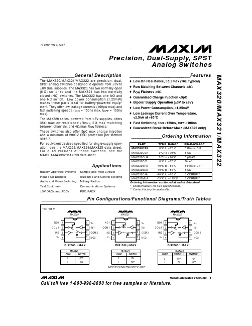
MAX320-MAX322中文资料
ELECTRICAL CHARACTERISTICS
(V+ = +5V ±10%, V- = -5V ±10%, VINH = 3.5V, VINL = 2.5V, TA = TMIN to TMAX, unless otherwise noted.)
PARAMETER ANALOG SWITCH Analog Signal Range
For equivalent devices specified for single-supply operation, see the MAX323/MAX324/MAX325 data sheet. For quad versions of these switches, see the MAX391/MAX392/MAX393 data sheet.
Plastic DIP (derate 9.09mW/°C above +70°C) .............727mW Narrow SO (derate 5.88mW/°C above +70°C) .............471mW
µMAX (derate 4.10mW/°C above +70°C) .....................330mW CERDIP (derate 8.00mW/°C above +70°C) ..................640mW Operating Temperature Ranges MAX32_C_ _ ........................................................0°C to +70°C MAX32_E_ _......................................................-40°C to +85°C MAX32_MJA ...................................................-55°C to +125°C Storage Temperature Range .............................-65°C to +150°C Lead Temperature (soldering, 10sec) .............................+300°C
MAX15301数据手册中文版

MAX15301是一个全功能,高效,数字化的点负载(POL)操纵器与先进的电源治理和遥测功能与PID 为基础的数字电源稳压器,MAX15301采纳Maxim拥有专利的Intune的™自动补偿,状态空间操纵算法。
Intune 的操纵律是有效的小信号和大信号响应,占占空比饱和度的阻碍。
这排除需要用户以确信和设置的阈值从线性转换到非线性模式。
这些能力在快速环路的瞬态响应,并减少输出电容器的数量相较,竞争的模拟和数字操纵器。
MAX15301包括多种功能,以优化效率。
内部开关BabyBuck的稳压器可产生栅极驱动器和内部偏置电源,低功耗的操纵器。
一种先进的,高效率的MOSFET的栅极驱动器,具有自适应非重叠按时,而持续调整的高侧和低侧的按时和驱动电压的全范围内的电压,电流和温度,以尽可能减少开关损耗。
MAX15301设计最终客户的设计环境的初衷。
上的PMBus™兼容的串行总线接口进行通信的监控器监控和故障治理。
全套的电源治理功能,无需复杂和昂贵的测序和监控IC。
大体的DC-DC转换操作,可设置通过引脚搭接,并非需要用户配置固件。
这使得电源子系统的快速进展前完成板级系统的工程。
Maxim提供支持的硬件和软件配置MAX15301 ,MAX15301可在32引线,5mm×5mm TQFN封装,工作在-40°C至+85°C的温度范围内。
特点:的自动补偿功能能够确保稳固,同时优化瞬态性能2.在快速瞬态响应减少输出电容的非线性补偿结果3.差分远端电压传感许诺±1%V OUT精度在整个温度范围内(-40°C至+85°C)接口用于配置,操纵和监测5.支持电压定位6.提高效率(自适应非重叠时序驱动器)至14V的宽输入电压范围8.高效片上BabyBuck稳压器的自偏置9.输出电压范围从到10.进入预偏置输出启动11.可配置的软启动和软停止时刻12.固定工作频率同步(300kHz至1MHz)13.灵活的排序和故障治理14.引脚手动跳线配置(输出电压,从机地址,开关频率,电流限制)15.能够快速原型图表典型工作电路引脚名字功能1SYNC外部开关频率同步输入端。
MAX13103 芯片数据手册说明书

MJD200 (NPN),MJD210 (PNP)Complementary Plastic Power TransistorsNPN/PNP Silicon DPAK For Surface Mount ApplicationsDesigned for low voltage, low−power, high−gain audio amplifier applications.Features•High DC Current Gain•Lead Formed for Surface Mount Applications in Plastic Sleeves (No Suffix)•Low Collector−Emitter Saturation V oltage•High Current−Gain − Bandwidth Product•Annular Construction for Low Leakage •EpoxyMeetsUL94V−*********•NJV Prefix for Automotive and Other Applications Requiring Unique Site and Control Change Requirements; AEC−Q101 Qualified and PPAP Capable•These Devices are Pb−Free and are RoHS CompliantMAXIMUM RATINGSRating Symbol Max UnitCollector−Base Voltage V CB40VdcCollector−Emitter Voltage V CEO25VdcEmitter−Base Voltage V EB8.0VdcCollector Current − Continuous I C 5.0AdcCollector Current − Peak I CM10AdcBase Current I B 1.0AdcTotal Power Dissipation @ T C = 25°C Derate above 25°C P D12.50.1WW/°CTotal Power Dissipation (Note 1) @ T A = 25°CDerate above 25°C P D1.40.011WW/°COperating and Storage JunctionTemperature RangeT J, T stg−65 to +150°C ESD − Human Body Model HBM3B V ESD − Machine Model MM C V Stresses exceeding Maximum Ratings may damage the device. Maximum Ratings are stress ratings only. Functional operation above the Recommended Operating Conditions is not implied. Extended exposure to stresses above the Recommended Operating Conditions may affect device reliability.1.These ratings are applicable when surface mounted on the minimum padsizes recommended.SILICONPOWER TRANSISTORS5 AMPERES25 VOLTS, 12.5 WATTSDPAKCASE 369CSTYLE 1MARKING DIAGRAMA= Assembly LocationY=YearWW=Work Weekx= 1 or 0G=Pb−Free PackageAYWWJ2x0GSee detailed ordering and shipping information in the package dimensions section on page 6 of this data sheet.ORDERING INFORMATION1BASE3EMITTERCOLLECTOR2,412341BASE3EMITTERCOLLECTOR2,4PNP NPNTHERMAL CHARACTERISTICSCharacteristic Symbol Max Unit Thermal Resistance, Junction−to−Case R q JC10°C/W Thermal Resistance, Junction−to−Ambient (Note 2)R q JA89.3°C/W 2.These ratings are applicable when surface mounted on the minimum pad sizes recommended.ELECTRICAL CHARACTERISTICS(T C = 25°C unless otherwise noted)Characteristic Symbol Min Max Unit OFF CHARACTERISTICSCollector−Emitter Sustaining Voltage (Note 3) (I C = 10 mAdc, I B = 0)V CEO(sus)25−VdcCollector Cutoff Current(V CB = 40 Vdc, I E = 0)(V CB = 40 Vdc, I E = 0, T J = 125°C)V CBO−−100100nAdcm AdcEmitter Cutoff Current (V BE = 8 Vdc, I C = 0)V EBO−100nAdcON CHARACTERISTICSC Current Gain (Note 3),(I C = 500 mAdc, V CE = 1 Vdc) (I C = 2 Adc, V CE = 1 Vdc)(I C = 5 Adc, V CE = 2 Vdc)h FE704510−180−−Collector−Emitter Saturation Voltage (Note 3) (I C = 500 mAdc, I B = 50 mAdc)(I C = 2 Adc, I B = 200 mAdc)(I C = 5 Adc, I B = 1 Adc)V CE(sat)−−−0.30.751.8VdcBase−Emitter Saturation Voltage (Note 3) (I C = 5 Adc, I B = 1 Adc)V BE(sat)− 2.5VdcBase−Emitter On Voltage (Note 3) (I C = 2 Adc, V CE = 1 Vdc)V BE(on)− 1.6VdcDYNAMIC CHARACTERISTICSCurrent−Gain − Bandwidth Product (Note 4)(I C = 100 mAdc, V CE = 10 Vdc, f test = 10 MHz)f T65−MHzOutput Capacitance(V CB = 10 Vdc, I E = 0, f = 0.1 MHz)MJD200MJD210, NJVMJD210T4G C ob−−80120pF3.Pulse Test: Pulse Width = 300 m s, Duty Cycle [ 2%.4.f T = ⎪h fe⎪• f test.Figure 1. Power DeratingT, TEMPERATURE (°C)T CPD,POWERDISSIPATION(WATTS)Figure 2. Switching Time Test Circuit2.51.51T A0.520SCOPEV CCt r, t f≤ 10 nsDUTY CYCLE = 1%D1 MUST BE FAST RECOVERY TYPE, e.g.: 1N5825 USED ABOVE I B≈ 100 mA MSD6100 USED BELOW I B≈ 100 mAR B and R C VARIED TO OBTAIN DESIRED CURRENT LEVELSFOR PNP TEST CIRCUIT,REVERSE ALL POLARITIESI C, COLLECTOR CURRENT (A)1KI C, COLLECTOR CURRENT (A)t,TIME(ns)50030020010050302010510.02Figure 3. Turn−On Time Figure 4. Turn−Off Timet,TIME(ns)32I C , COLLECTOR CURRENT (A)I C , COLLECTOR CURRENT (A)I C , COLLECTOR CURRENT (A)h F E , D C C U R R E N T G A I NFigure 5. DC Current GainFigure 6. “On” VoltageI C , COLLECTOR CURRENT (A)200400100806040IC , COLLECTOR CURRENT (A)Figure 7. Temperature Coefficients202I C , COLLECTOR CURRENT (A)1.61.20.80.4V , V O L T AG E (V O L T S )NPN MJD200PNP MJD210h F E , D C C U R R E N T G A I NV , V O L T A G E (V O L T S )21.61.20.80.4V , T E M P E R A T U R E C O E F F I C I E N T S (m V /C )°θ+ 2.5+ 2+ 1.5+ 10- 0.5- 1- 1.5- 2+ 0.5- 2.5V , T E M P E R A T U R E C O E F F I C I E N T S (m V /C )°θ+ 2.5+ 2+ 1.5+ 10- 0.5- 1- 1.5- 2+ 0.5- 2.5t, TIME (ms)r (t ), T R A N S I E N T T H E R M A L R E S I S T A N C E (N O R M A L I Z E D )Figure 8. Thermal ResponseV CE , COLLECTOR−EMITTER VOLTAGE (V)25Figure 9. Active Region Safe Operating Area13I C , C O LL E C T O R C U R R E N T (A M P )There are two limitations on the power handling ability of a transistor: average junction temperature and second breakdown. Safe operating area curves indicate I C − V CE limits of the transistor that must be observed for reliable operation; i.e., the transistor must not be subjected to greater dissipation than the curves indicate.The data of Figure 9 is based on T J(pk) = 150°C; T C is variable depending on conditions. Second breakdown pulse limits are valid for duty cycles to 10% provided T J(pk)≤ 150°C. T J(pk) may be calculated from the data in Figure 8.At high case temperatures, thermal limitations will reduce the power that can be handled to values less than the limitations imposed by second breakdown.200V R , REVERSE VOLTAGE (V)207010030Figure 10. Capacitance50C , C A P A C I T A N C E (p F )ORDERING INFORMATIONDevice Package Type Shipping†75 Units / RailMJD200G DPAK(Pb−Free)1,800 / Tape & ReelMJD200RLG DPAK(Pb−Free)2,500 / Tape & ReelMJD200T4G DPAK(Pb−Free)75 Units / RailMJD210G DPAK(Pb−Free)1,800 / Tape & ReelMJD210RLG DPAK(Pb−Free)2,500 / Tape & ReelMJD210T4G DPAK(Pb−Free)2,500 / Tape & ReelNJVMJD210T4G*DPAK(Pb−Free)†For information on tape and reel specifications, including part orientation and tape sizes, please refer to our Tape and Reel Packaging Specifications Brochure, BRD8011/D.*NJV Prefix for Automotive and Other Applications Requiring Unique Site and Control Change Requirements; AEC−Q101 Qualified and PPAP CapablePACKAGE DIMENSIONSDPAK CASE 369C ISSUE DSTYLE 1:PIN 1.BASE2.COLLECTOR3.EMITTER4.COLLECTORǒmm inchesǓSCALE 3:1*For additional information on our Pb−Free strategy and solderingdetails, please download the ON Semiconductor Soldering and Mounting Techniques Reference Manual, SOLDERRM/D.SOLDERING FOOTPRINT*DIM MIN MAX MIN MAX MILLIMETERSINCHES D 0.2350.245 5.97 6.22E 0.2500.265 6.35 6.73A 0.0860.094 2.18 2.38b 0.0250.0350.630.89c20.0180.0240.460.61b20.0300.0450.76 1.14c 0.0180.0240.460.61e 0.090 BSC 2.29 BSC b30.1800.215 4.57 5.46L4−−−0.040−−− 1.01L 0.0550.070 1.40 1.78L30.0350.0500.89 1.27Z0.155−−−3.93−−−NOTES:1.DIMENSIONING AND TOLERANCING PER ASME Y14.5M, 1994.2.CONTROLLING DIMENSION: INCHES.3.THERMAL PAD CONTOUR OPTIONAL WITHIN DI-MENSIONS b3, L3 and Z.4.DIMENSIONS D AND E DO NOT INCLUDE MOLD FLASH, PROTRUSIONS, OR BURRS. MOLDFLASH, PROTRUSIONS, OR GATE BURRS SHALL NOT EXCEED 0.006 INCHES PER SIDE.5.DIMENSIONS D AND E ARE DETERMINED AT THE OUTERMOST EXTREMES OF THE PLASTIC BODY .6.DATUMS A AND B ARE DETERMINED AT DATUM PLANE H.H 0.3700.4109.4010.41A10.0000.0050.000.13L10.108 REF 2.74 REF L20.020 BSC 0.51 BSC DETAIL AROTATED 90 CW 5ON Semiconductor and are registered trademarks of Semiconductor Components Industries, LLC (SCILLC). SCILLC owns the rights to a number of patents, trademarks,copyrights, trade secrets, and other intellectual property. A listing of SCILLC’s product/patent coverage may be accessed at /site/pdf/Patent−Marking.pdf. SCILLC reserves the right to make changes without further notice to any products herein. SCILLC makes no warranty, representation or guarantee regarding the suitability of its products for any particular purpose, nor does SCILLC assume any liability arising out of the application or use of any product or circuit, and specifically disclaims any and all liability, including without limitation special, consequential or incidental damages. “Typical” parameters which may be provided in SCILLC data sheets and/or specifications can and do vary in different applications and actual performance may vary over time. All operating parameters, including “Typicals” must be validated for each customer application by customer’s technical experts. SCILLC does not convey any license under its patent rights nor the rights of others. SCILLC products are not designed, intended, or authorized for use as components in systems intended for surgical implant into the body, or other applications intended to support or sustain life, or for any other application in which the failure of the SCILLC product could create a situation where personal injury or death may occur. Should Buyer purchase or use SCILLC products for any such unintended or unauthorized application, Buyer shall indemnify and hold SCILLC and its officers, employees, subsidiaries, affiliates, and distributors harmless against all claims, costs, damages, and expenses, and reasonable attorney fees arising out of, directly or indirectly,any claim of personal injury or death associated with such unintended or unauthorized use, even if such claim alleges that SCILLC was negligent regarding the design or manufacture of the part. SCILLC is an Equal Opportunity/Affirmative Action Employer. This literature is subject to all applicable copyright laws and is not for resale in any manner.PUBLICATION ORDERING INFORMATION。
MAX913中文资料
M A X912/M A X913————单/双路,超高速,低功耗,精密的TTL比较器1.总体描述MAX913(单)和MAX912(双)高速,低功耗比较器是一个拥有独特设计就是在其线性区域是它的比较是可以防止振荡。
没有要求最低输入转换率。
它是由差分输入和互补的TTL输出。
快速传播延迟(10ns的典型值),具有极低的电源电流和宽共模输入范围,包括负电流使MAX912/MAX913达到的低功耗理想效果,高速,单电源+5V(或±5V)的应用,例如有V/F转换器和开关稳压器。
MAX912/MAX913保持着稳定的线性区域输出。
此功能消除了常见的在输出不稳定时产生高速驱动时具有的比较滞销输入信号。
该MAX912/MAX913可以单一+5V电源供电或±5V的分别供应。
该MAX913是一个改进的LT1016的替代品。
在输入一小能量时它提供了更宽的输入电压范围和等效速度。
在MAX912双比较具有同等性能的MAX913并且包括独立的锁存控制功能。
2.应用过零检测器以太网线接收器开关稳压器高速采样电路高速触发器扩展范围的V/F转换器快速脉冲宽度/高度的判别3.特点超快速(为10ns)单+5V或±5V的双电源供电输入范围扩展至负电源以下低功耗:6毫安(+5V)的每次比较无最小输入信号摆率的要求无电源电流扣球稳定的线性区可投入任一电源低失调电压:0.8mV4.引脚配置顶视图:5.绝对最大额定值:正电源电压 (7V)负电源电压..............................................-7V差分输入电压.......................................±15V输入电压....................................-0.3V至15V锁存引脚电压...................................等于耗材连续输出电流.....................................±20mA连续功耗(TA=70℃)8引脚塑料DIP(减少9.09mW/妹高于70°)......727mW 8引脚SO(减少5.88mW/每高于70°).................471mW 8引脚CERDIP(减少8.00mW/每高于70°).........640mW 16引脚塑料DIP(减少10.53mW/高于70°).......842mW 16引脚窄的SO(减免8.70mW/高于70°)..........696mW16引脚CERDIP(减免10.00mW/高于70°)..........800mW工作温度范围:MAX91C......................................................0℃至70℃MAX91E....................................................-40℃至85℃MAX91MJ.................................................-55℃至125℃储存温度范围........................................-65°C至150°C焊接温度(10秒).........................................................300℃注:超越“绝对最大额定值“,即可能造成永久性损坏设备。
- 1、下载文档前请自行甄别文档内容的完整性,平台不提供额外的编辑、内容补充、找答案等附加服务。
- 2、"仅部分预览"的文档,不可在线预览部分如存在完整性等问题,可反馈申请退款(可完整预览的文档不适用该条件!)。
- 3、如文档侵犯您的权益,请联系客服反馈,我们会尽快为您处理(人工客服工作时间:9:00-18:30)。
General DescriptionThe MAX16010–MAX16014 is a family of ultra-small, low-power, overvoltage protection circuits for high-voltage,high-transient systems such as those found in automotive,telecom, and industrial applications. These devices oper-ate over a wide 5.5V to 72V supply voltage range, making them also suitable for other applications such as battery stacks, notebook computers, and servers.The MAX16010 and MAX16011 offer two independent comparators for monitoring both undervoltage and overvoltage conditions. These comparators offer open-drain outputs capable of handling voltages up to 72V.The MAX16010 features complementary enable inputs (EN/EN ), while the MAX16011 features an active-high enable input and a selectable active-high/low OUTB output.The MAX16012 offers a single comparator and an inde-pendent reference output. The reference output can be directly connected to either the inverting or noninverting input to select the comparator output logic.The MAX16013 and MAX16014 are overvoltage protec-tion circuits that are capable of driving two p-channel MOSF ETs to prevent reverse-battery and overvoltage conditions. One MOSF ET (P1) eliminates the need for external diodes, thus minimizing the input voltage drop.The second MOSFET (P2) isolates the load or regulates the output voltage during an overvoltage condition. The MAX16014 keeps the MOSFET (P2) latched off until the input power is cycled.The MAX16010 and MAX16011 are available in small 8-pin TDFN packages, while the MAX16012/MAX16013/MAX16014 are available in small 6-pin TDFN packages.These devices are fully specified from -40°C to +125°C.ApplicationsAutomotive Industrial48V Telecom/Server/Networking FireWire ®Notebook ComputersMulticell Battery-Stack Powered EquipmentFeatures♦Wide 5.5V to 72V Supply Voltage Range♦Open-Drain Outputs Up to 72V (MAX16010/MAX16011/MAX16012)♦Fast 2µs (max) Propagation Delay ♦Internal Undervoltage Lockout♦p-Channel MOSFET Latches Off After an Overvoltage Condition (MAX16014)♦Adjustable Overvoltage Threshold♦-40°C to +125°C Operating Temperature Range ♦Small 3mm x 3mm TDFN PackageMAX16010–MAX16014Ultra-Small, Overvoltage Protection/Detection Circuits________________________________________________________________Maxim Integrated Products 1Ordering InformationTypical Operating Circuit19-3693; Rev 2; 1/07For pricing, delivery, and ordering information,please contact Maxim/Dallas Direct!at 1-888-629-4642, or visit Maxim’s website at .hysteresis, and “C” for 7.5% hysteresis.FireWire is a registered trademark of Apple Computer, Inc.Pin Configurations appear at end of data sheet.*Replace -T with +T for lead-free packages.**EP = Exposed pad.M A X 16010–M A X 16014Ultra-Small, Overvoltage Protection/Detection Circuits 2_______________________________________________________________________________________ABSOLUTE MAXIMUM RATINGSELECTRICAL CHARACTERISTICS(V CC = 14V, T A = -40°C to +125°C, unless otherwise noted. Typical values are at T A = +25°C.) (Note 1)Stresses beyond those listed under “Absolute Maximum Ratings” may cause permanent damage to the device. These are stress ratings only, and functional operation of the device at these or any other conditions beyond those indicated in the operational sections of the specifications is not implied. Exposure to absolute maximum rating conditions for extended periods may affect device reliability.(All pins referenced to GND, unless otherwise noted.)V CC .........................................................................-0.3V to +80V EN, EN , LOGIC...........................................-0.3V to (V CC + 0.3V)INA+, INB-, IN+, IN-, REF, SET..............................-0.3V to +12V OUTA, OUTB, OUT.................................................-0.3V to +80V GATE1, GATE2 to V CC ...........................................-12V to +0.3V GATE1, GATE2...........................................-0.3V to (V CC + 0.3V)Current Sink/Source (all pins).............................................50mAContinuous Power Dissipation (T A = +70°C)6-Pin TDFN (derate 18.2mW/°C above +70°C).........1455mW 8-Pin TDFN (derate 18.2mW/°C above +70°C).........1455mW Operating Temperature Range .........................-40°C to +125°C Maximum Junction Temperature.....................................+150°C Storage Temperature Range.............................-60°C to +150°C Lead Temperature (soldering, 10s).................................+300°CMAX16010–MAX16014Ultra-Small, Overvoltage Protection/Detection Circuits_______________________________________________________________________________________3ELECTRICAL CHARACTERISTICS (continued)(V CC = 14V, T A = -40°C to +125°C, unless otherwise noted. Typical values are at T A = +25°C.) (Note 1)A A A Typical Operating Characteristics(V IN = 14V, T A = +25°C, unless otherwise noted.)SUPPLY CURRENT vs. SUPPLY VOLTAGESUPPLY VOLTAGE (V)S U P P L Y C U R R E N T (µA )65554535251515202530354010575SUPPLY CURRENT vs. TEMPERATURETEMPERATURE (°C)S U P P L Y C U R R E N T (µA )110956580-105203550-2526.0526.1026.1526.2026.2526.3026.3526.4026.4526.5026.00-40125GATE VOLTAGE vs. SUPPLY VOLTAGESUPPLY VOLTAGE (V)G A T E V O L T A G E (V )6555453525151020304050600575M A X 16010–M A X 16014Ultra-Small, Overvoltage Protection/Detection Circuits 4_______________________________________________________________________________________Typical Operating Characteristics (continued)(V IN = 14V, T A = +25°C, unless otherwise noted.)UVLO THRESHOLD vs. TEMPERATURETEMPERATURE (°C)U V L O T H R E S H O L D (V )110956580-105203550-254.64.74.84.95.05.15.25.35.45.54.5-40125INA+/INB-/SET THRESHOLDvs. TEMPERATURETEMPERATURE (°C)I N A +/I N B -/S E T T H R E S H O L D (V )110956580-105203550-251.211.221.231.241.251.261.271.281.291.301.20-40125GATE VOLTAGE vs. TEMPERATURETEMPERATURE (°C)(V C C - V G A T E ) (V )110956580-105203550-259.19.29.39.49.59.69.79.89.910.09.0-40125STARTUP WAVEFORM(R OUT = 100Ω, C IN = 10µF, C OUT = 10nF)MAX16010 toc07V GATE 5V/div V OUT 10V/divV CC 10V/div200µs/divSTARTUP WAVEFORM(R OUT = 100Ω, C IN = 10µF, C OUT = 10nF)V GATE 10V/divV OUT 10V/divV CC 1V/div20µs/divV EN = 0 TO 2VOVERVOLTAGE SWITCH FAULT(R OUT = 100Ω, C IN = 80µF, C OUT = 10nF)V GATE 20V/divV OUT 20V/divV CC 20V/div 1ms/divV IN = 12V TO 40V, TRIP THRESHOLD = 28VOVERVOLTAGE LIMIT(R OUT = 100Ω, C IN = 80µF, C OUT = 10nF)V GATE 20V/divV OUT 20V/divV CC 20V/div 1ms/divV IN = 12V TO 40VTRIP THRESHOLD = 28VMAX16010–MAX16014Ultra-Small, Overvoltage Protection/Detection CircuitsPin DescriptionM A X 16010–M A X 16014Detailed DescriptionThe MAX16010–MAX16014 is a family of ultra-small, low-power, overvoltage protection circuits for high-voltage,high-transient systems such as those found in automo-tive, telecom, and industrial applications. These devices operate over a wide 5.5V to 72V supply voltage range,making them also suitable for other applications such as battery stacks, notebook computers, and servers.The MAX16010 and MAX16011 offer two independent comparators for monitoring both undervoltage and overvoltage conditions. These comparators offer open-drain outputs capable of handling voltages up to 72V.The MAX16010 features complementary enable inputs (EN/EN ), while the MAX16011 features an active-high enable input and a selectable active-high/low OUTB output.The MAX16012 offers a single comparator and an inde-pendent reference output. The reference output can be directly connected to either the inverting or noninvert-ing input to select the comparator output logic.The MAX16013 and MAX16014 are overvoltage protec-tion circuits that are capable of driving two p-channel MOSF ETs to prevent reverse battery and overvoltage conditions. One MOSF ET (P1) eliminates the need for external diodes, thus minimizing the input voltage drop.While the second MOSFET (P2) isolates the load or reg-ulates the output voltage during an overvoltage condi-tion. The MAX16014 keeps the MOSF ET (P2) latched off until the input power is cycled.Voltage MonitoringThe MAX16010/MAX16011 include undervoltage and overvoltage comparators for window detection (see Figure 1). OUT_ asserts high when the monitored volt-age is within the selected “window.” OUTB asserts low when the monitored voltage falls below the lower (V TRIPLOW ) limit of the window, or OUTA asserts low if the monitored voltage exceeds the upper limit (V TRIPHIGH ). The application in F igure 1 shows OUT_enabling the DC-DC converter when the monitored volt-age is in the selected window.The resistor values R1, R2, and R3 can be calculated as follows:TOTAL Use the following steps to determine the values for R1,R2, and R3.1)Choose a value for R TOTAL , the sum of R1, R2, and R3. Because the MAX16010/MAX16011 have very high input impedance, R TOTAL can be up to 5M Ω.2)Calculate R3 based on R TOTAL and the desired upper trip point:3)Calculate R2 based on R TOTAL , R3, and the desired lower trip point:4)Calculate R1 based on R TOTAL , R3, and R2:R1 = R TOTAL - R2 - R3The MAX16012 has both inputs of the comparator avail-able with an integrated 1.30V reference (REF). When the voltage at IN+ is greater than the voltage at IN- then OUT goes high. When the voltage at IN- is greater than the voltage at IN+ then OUT goes low. Connect REF to IN+or IN- to set the reference voltage value. Use an external resistive divider to set the monitored voltage threshold.Ultra-Small, Overvoltage Protection/Detection Circuits 6_______________________________________________________________________________________The MAX16013/MAX16014 can be configured as an overvoltage switch controller to turn on/off a load (see the Typical Application Circuit ). When the programmed overvoltage threshold is tripped, the internal fast com-parator turns off the external p-channel MOSF ET (P2),pulling GATE2 to V CC to disconnect the power source from the load. When the monitored voltage goes below the adjusted overvoltage threshold, the MAX16013enhances GATE2, reconnecting the load to the power source (toggle ENABLE on the MAX16014 to reconnect the load). The MAX16013 can be configured as an overvoltage limiter switch by connecting the resistive divider to the load instead of V CC (F igure 3). See the Overvoltage Limiter section.Supply VoltageConnect a 5.5V to 72V supply to V CC for proper opera-tion. For noisy environments, bypass V CC to GND with a 0.1µF or greater capacitor. When V CC falls below the UVLO voltage the following states are present (Table 1).HysteresisHysteresis adds noise immunity to the voltage monitors and prevents oscillation due to repeated triggering when the monitored voltage is near the threshold trip voltage. The hysteresis in a comparator creates two trip points: one for the rising input voltage (V TH+) and one for the falling input voltage (V TH-). These thresholds are shown in Figure 4.Enable Inputs (EN or EN )The MAX16011 offers an active-high enable input (EN),while the MAX16010 offers both an active-high enable input (EN) and active-low enable input (EN ). F or the MAX16010, drive EN low or EN high to force the output low. When the device is enabled (EN = high and EN =low) the state of OUTA and OUTB depends on INA+and INB- logic states.MAX16010–MAX16014Ultra-Small, Overvoltage Protection/Detection Circuits_______________________________________________________________________________________7Table 1. UVLO State (V CC < V UVLO )M A X 16010–M A X 16014OUTB low when LOGIC = low, and OUTB high when LOGIC = high. When the device is enabled (EN = high)the state of OUTA and OUTB depends on the INA+,INB-, and LOGIC input (see Table 2).F or the MAX16013/MAX16014, drive EN low to pull GATE2 to V CC , turning off the p-channel MOSFET (P2).When the device is enabled (EN = high), GATE2 is pulled to the greater of (V CC - 10V) or GND turning on the external MOSFET (P2).Applications InformationLoad DumpMost automotive applications are powered by a multi-cell, 12V lead-acid battery with a voltage between 9V and 16V (depending on load current, charging status,temperature, battery age, etc.). The battery voltage is distributed throughout the automobile and is locally regulated down to voltages required by the different system modules. Load dump occurs when the alterna-tor is charging the battery and the battery becomes disconnected. Power in the alternator inductance flows into the distributed power system and elevates the volt-age seen at each module. The voltage spikes have rise times typically greater than 5ms and decays within sev-eral hundred milliseconds but can extend out to 1s or more depending on the characteristics of the charging system. These transients are capable of destroying sensitive electronic equipment on the first fault event.The MAX16013/MAX16014 provide the ability to dis-connect the load from the charging system during an overvoltage condition to protect the module. In addi-tion, the MAX16013 can be configured in a voltage-lim-iting mode. This allows continuous operation while providing overvoltage protection. See the Overvoltage Limiter section.Input Transients ClampingWhen the external MOSF ET is turned off during an overvoltage occurrence, stray inductance in the power path may cause voltage ringing to exceed the MAX16013/MAX16014 absolute maximum input (V CC )supply rating. The following techniques are recom-mended to reduce the effect of transients:•Minimize stray inductance in the power path usingwide traces, and minimize loop area including the power traces and the return ground path.•Add a zener diode or transient voltage suppresser(TVS) rated below V CC absolute maximum rating (Figure 3).Overvoltage LimiterWhen operating in overvoltage-limiter mode, the MAX16013 drives the external p-channel MOSFET (P2),resulting in the external MOSFET operating as a voltage regulator.During normal operation, GATE2 is pulled to the greater of (V CC - 10V) or GND. The external MOSF ET’s drain voltage is monitored through a resistor-divider between the P2 output and SET. When the output voltage rises above the adjusted overvoltage threshold, an internal comparator pulls GATE2 to V CC . When the monitored voltage goes below the overvoltage threshold, the p-channel MOSF ET (P2) is turned on again. This process continues to keep the voltage at the output reg-ulated to within approximately a 5% window. The output voltage is regulated during the overvoltage transients and the MOSFET (P2) continues to conduct during the overvoltage event, operating in switched-linear mode.Caution must be exercised when operating the MAX16013 in voltage-limiting mode for long durations due to the MOSF ET’s power dissipation consideration (see the MOSFET Selection and Operation section).MOSFET Selection and Operation(MAX16013 and MAX16014)Most battery-powered applications must include reverse voltage protection. Many times this is implemented with a diode in series with the battery. The disadvantage in using a diode is the forward voltage drop of the diode,which reduces the operating voltage available to down-stream circuits (V LOAD = V BATTERY - V DIODE ). The MAX16013 and MAX16014 include high-voltage GATE1drive circuitry allowing users to replace the high-voltage-drop series diode with a low-voltage-drop MOSF ET device (as shown in the Typical Operating Circuit and Figure 3). The forward voltage drop is reduced to I LOAD x R DS-ON of P1. With a suitably chosen MOSF ET, the voltage drop can be reduced to millivolts.Ultra-Small, Overvoltage Protection/Detection Circuits 8_______________________________________________________________________________________Table 2. MAX16011 Output LogicIn normal operating mode, internal GATE1 output cir-cuitry enhances P1 to a 10V gate-to-source (V GS) for 11V < V CC< 72V. The constant 10V enhancement ensures P1 operates in a low R DS-ON mode, but the gate-source junction is not overstressed during high-battery-voltage application or transients (many MOSFET devices specify a ±20V V GS absolute maximum). As V CC drops below 10V GATE1 is limited to GND, reduc-ing P1 V GS to V CC- GND. In normal operation the P1 power dissipation is very low:P1 = I LOAD2x R DS-ONDuring reverse-battery applications, GATE1 is limited to GND and the P1 gate-source junction is reverse biased. P1 is turned off and neither the MAX16013/ MAX16014 nor the load circuitry is exposed to the reverse-battery voltage. Care should be taken to place P1 (and its internal drain-to-source diode) in the correct orientation for proper reverse battery operation.P2 protects the load from input overvoltage conditions. During normal operating modes (the monitored voltage is below the adjusted overvoltage threshold), internal GATE2 output circuitry enhances P2 to a 10V gate-to-source (V GS) for 11V < V CC< 72V. The constant 10V enhancement ensures P2 operates in a low R DS-ON mode but the gate-to-source junction is not over-stressed during high-battery-voltage applications (many pFET devices specify a ±20V V GS absolute max-imum). As V CC drops below 10V, GATE2 is limited to GND, reducing P2 V GS to V CC- GND. In normal opera-tion, the P2 power dissipation is very low:P2 = I LOAD2x R DS-ON During overvoltage conditions, P2 is either turned com-pletely off (overvoltage-switch mode) or cycled off-on-off (voltage-limiter mode). Care should be taken toplace P2 (and its internal drain-to-source diode) in the correct orientation for proper overvoltage protection operation. During voltage-limiter mode, the drain of P2is limited to the adjusted overvoltage threshold, whilethe battery (V CC) voltage rises. During prolonged over-voltage events, P2 temperature can increase rapidlydue to the high power dissipation. The power dissipat-ed by P2 is:P2 = V DS-P2 x I LOAD= (V CC- V OV-ADJUSTED) x I LOADwhere V CC~ V BATTERY and V OV-ADJUSTED is the desiredload limit voltage. For prolonged overvoltage events withhigh P2 power dissipation, proper heatsinking is required.Adding External Pullup ResistorsIt may be necessary to add an external resistor fromV CC to GATE1 to provide enough additional pullup capability when the GATE1 input goes high. The GATE_ output can only source up to 1µA current. If the source current is less than 1µA, no external resistormay be necessary. However, to improve the pullup capability of the GATE_ output when it goes high, con-nect an external resistor between V CC and the GATE_.The application shows a 2MΩresistor, which is large enough not to impact the sinking capability of the GATE_ (during normal operation) while providing enough pullup during an overvoltage event. With an11V (worst case) V CC-to-gate clamp voltage and a sinking current of 75µA, the smallest resistor should be11V/75µA, or about 147kΩ. However, since the GATE_is typically low most of the time, a higher value shouldbe used to reduce overall power consumption.MAX16010–MAX16014Ultra-Small, Overvoltage Protection/Detection Circuits _______________________________________________________________________________________9M A X 16010–M A X 16014Ultra-Small, Overvoltage Protection/Detection Circuits 10MAX16010–MAX16014Ultra-Small, Overvoltage Protection/Detection Circuits______________________________________________________________________________________11Chip InformationPROCESS: BiCMOSPin ConfigurationsM A X 16010–M A X 16014Ultra-Small, Overvoltage Protection/Detection Circuits Maxim cannot assume responsibility for use of any circuitry other than circuitry entirely embodied in a Maxim product. No circuit patent licenses are implied. Maxim reserves the right to change the circuitry and specifications without notice at any time.12____________________Maxim Integrated Products, 120 San Gabriel Drive, Sunnyvale, CA 94086 408-737-7600©2007 Maxim Integrated Productsis a registered trademark of Maxim Integrated Products, Inc.Package Information(The package drawing(s) in this data sheet may not reflect the most current specifications. For the latest package outline information,go to /packages .)Revision HistoryPages changed at Rev 2: 1, 10, 12。